
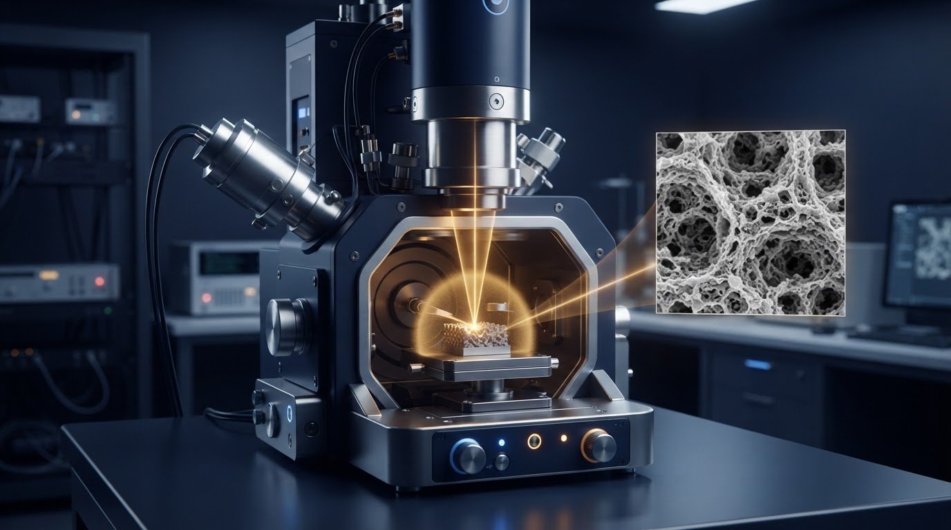
A smaller SEM spot can sharpen fine detail, but it is not automatically the best setting. Understanding SEM spot size means balancing probe diameter and beam current: a smaller aperture can reduce probe diameter and improve resolution, while a larger aperture increases current and signal-to-noise but may soften fine detail. For benchtop SEM imaging, choose settings based on what the sample needs to reveal.
It is natural to expect higher magnification or a stronger signal to produce a clearer image. In practice, magnification enlarges the image, while spot size and related beam settings determine whether the detail is resolved clearly. Increasing beam intensity can also increase spot size, creating a trade-off between image sharpness and signal.
This guide explains how spot size relates to probe diameter and beam current, how beam settings affect contrast and sharpness, and why magnification does not always reveal more surface detail. It also shows how these principles apply to benchtop SEMs, where matching imaging conditions to the sample and feature of interest is central to obtaining useful results.
Key Takeaways
- Match beam current to the sample and imaging goal to balance usable signal with surface preservation.
- Distinguish increased magnification from genuinely resolved detail by considering the feature size and image context.
- Understand how condenser and objective lens currents shape probe diameter and influence the final image.
- Apply these principles to benchtop SEM imaging by selecting settings around the details you need to observe.
Effects of electron beam settings on image contrast and sharpness
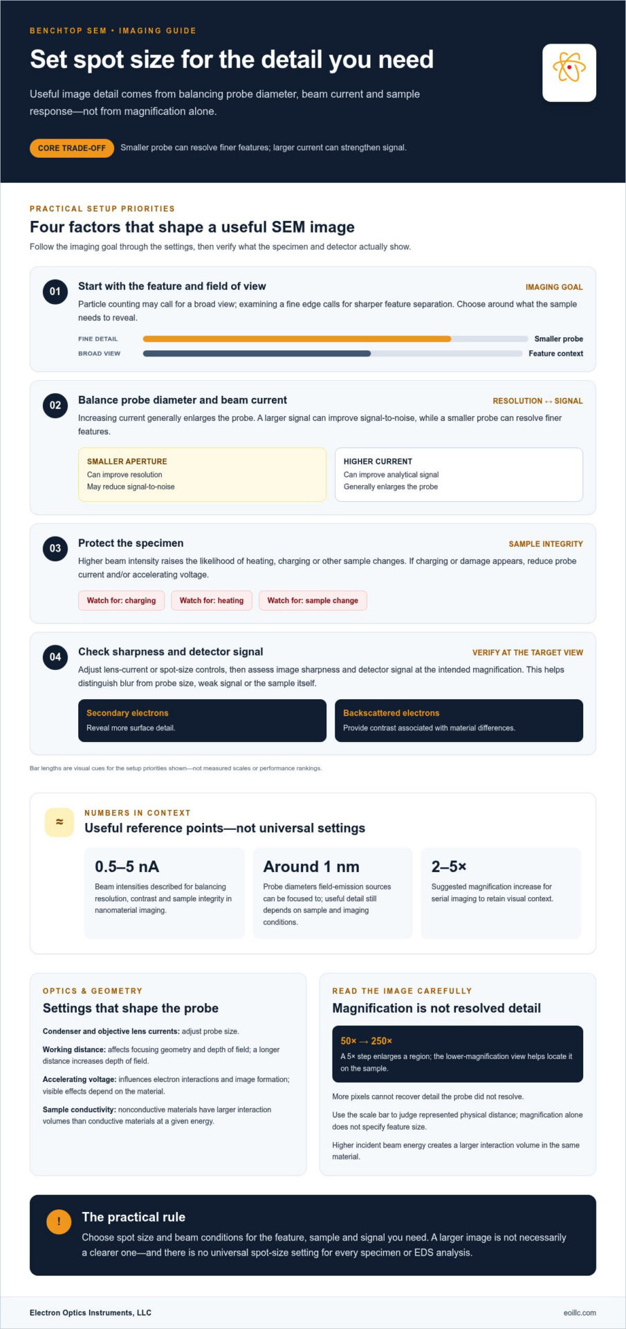
SEM image quality depends on balancing probe diameter and beam current. These settings influence resolution, contrast, and the signal collected during scanning.
Spot Size and Image Resolution
SEM spot size is the focused electron-probe diameter at the sample, and a smaller probe can resolve finer features. Field-emission sources can be focused to probe diameters around 1 nm, although the useful detail also depends on the sample and imaging conditions. Spot size differs from pixel size: pixels are sampling points in the digital image, while the probe interacts with the specimen. More pixels cannot recover detail the probe fails to resolve.
Probe Diameter and Beam Current
Probe diameter and beam current are linked: increasing current generally enlarges the probe, while a larger signal can improve signal-to-noise ratio. For nanomaterial imaging, beam intensities of 0.5-5 nA provide a balance among resolution, contrast, and sample integrity. High-resolution imaging therefore favors a smaller probe and sufficient signal; EDS analysis generally benefits from higher current for analytical signal. There is no universal spot-size setting for EDS, because sample and analysis conditions matter. Higher intensity also raises the likelihood of heating, charging, or other sample changes.
Factors That Determine Spot Size
Condenser and objective lens currents adjust probe size, while aperture selection balances current against diameter: a smaller aperture can improve resolution but reduce signal-to-noise. Working distance affects focusing geometry and depth of field; a longer distance increases depth of field. Accelerating voltage influences electron interactions and image formation, so its effect on visible detail depends on the material. Probe diameter is commonly expressed in nanometers, while beam current is measured in nA. Estimate actual probe size with a calibrated reference specimen, not from image pixel size alone.
Spot Size Settings and Image Formation
Adjust spot size using the SEM’s lens-current or spot-size controls, then assess image sharpness and detector signal at the intended magnification. During scanning, the electron beam moves across the specimen, and a detector collects signals such as secondary electrons, which reveal surface detail, to form image contrast. If charging or damage appears, reduce probe current and/or accelerating voltage. This characterization helps determine whether blur comes from probe size, weak signal, or the sample itself.
Magnification and visible surface detail
Magnification enlarges the scanned image, but enlargement alone cannot reveal detail the microscope has not resolved. In scanning electron microscopy, useful clarity depends on how the signal represents the surface, the probe conditions, and the interaction volume within the specimen. A highly magnified image can therefore appear larger without showing additional physical information.
For serial imaging, increase magnification by about 2-5X at a time to retain visual context. A change from 50X to 250X illustrates a 5X step: the second view enlarges a region, while the first helps locate it on the sample. This progression makes it easier to connect a local feature with the larger surface structure.
Read the scale bar alongside the displayed magnification. For example, an image marked 1,500× with a 30 μm scale bar shows the physical distance represented by that bar; the magnification label alone doesn’t specify the size of a feature. The scale bar is calibrated for each magnification, so it provides a more useful reference when comparing images.
Signal choice also shapes visible detail. Secondary electrons, which have less energy than backscattered electrons, reveal more surface detail. Backscattered-electron imaging provides contrast associated with material differences, so the preferred signal depends on whether surface form or compositional variation matters most. Detector response and signal generation both affect the final image.
Interaction volume adds another limit. Higher incident beam energy creates a larger interaction volume in the same material, and nonconductive materials have larger interaction volumes than conductive materials at a given energy. This can make the image represent a deeper region rather than only the outermost surface. Tabletop scanning electron microscopes can reach magnifications up to 100,000X for basic applications, but selecting magnification should begin with the feature and field of view needed, not the largest available value.
SEMs can resolve details hundreds of thousands of times smaller than optical microscopes, while the human eye can resolve features about 0.2 millimeters in size.
The image annotation x1.50k indicates that the image is magnified 1,500 times. FE SEMs and UHR FE SEMs provide magnifications from 10X up to 1,000,000X, though enlargement should still be chosen for the feature and field of view.
Benchtop SEM spot size
In benchtop SEM imaging, spot size is best chosen around the sample feature and the signal required, not a target magnification alone. A particle-counting task, for example, may need a broad field of view, while examining a fine edge calls for sharper feature separation. Tabletop SEM systems can provide magnification up to 100,000X for basic applications, but that maximum doesn’t guarantee useful detail on every specimen.
Sample preparation influences how the electron beam interacts with the surface. Conductive and nonconductive materials produce different interaction volumes at the same beam energy, with nonconductive samples having larger volumes. A thin nonconductive film on a conductive substrate can behave differently from a bulk insulating specimen. These differences affect which structures contribute to the image and how clearly surface features appear.
Match beam intensity to sample sensitivity and imaging purpose. For biological samples, beam intensities below 1 nA help minimize damage and charging. Metallurgical samples may use 1-10 nA for imaging and compositional information. These are application ranges, not universal presets: the desired signal, material response, and visible feature all shape the setting. Excessive intensity can cause local heating and alter sample morphology or composition.
Assess the image at the magnification and field of view needed for the task. If edges appear indistinct, consider whether the desired structure is smaller than the effective probe or obscured by signal from a larger interaction volume. If the image is noisy, more beam current may improve the signal, but it can also compromise fine resolution or affect sensitive samples. To address charging, reducing probe current or accelerating voltage can help; fast imaging with frame averaging can reduce noise. This balance helps a benchtop electron microscope produce images suited to surface inspection and sample characterization.
How is SEM spot size related to probe diameter and beam current?
SEM spot size describes the electron probe’s diameter where it reaches the specimen. A smaller probe can distinguish finer features, while beam current determines how many electrons contribute to the signal. These linked properties shape image detail and signal quality, so spot size is not simply a measure of sharpness. Understanding SEM spot size means considering both probe dimensions and the signal required for the task.
Condenser and objective lens currents adjust the probe by controlling electron-beam focusing. Typical electron-lens demagnification in a scanning electron microscope is on the order of 10-100, reducing the source image to a focused probe. Raising probe current generally increases probe diameter; the stronger signal can improve signal-to-noise, but the larger probe may blur nearby structures. A smaller aperture can narrow the probe, while lowering current and signal.
The final probe diameter reflects several physical effects, not a single lens setting. Spherical, chromatic, astigmatic, and diffraction contributions combine in quadrature: dp2 = ds2 + dc2 + dA2 + dd2. This relationship explains why reducing one contribution may not remove blur if another remains dominant. A clear understanding of SEM spot size helps connect those optical contributions to the probe formed at the sample.
Beam current is commonly measured in nanoamperes (nA). Choose the current based on the required image signal and feature scale, then assess whether the probe preserves the edges you need to resolve. For example, a weak image signal may call for more current, but increasing it can broaden the probe and reduce fine-detail separation. The best balance depends on the specimen’s response and the imaging purpose.
When comparing instruments, consider how lens controls, apertures, and current settings support the imaging conditions your work requires. Explore SEM instrument options to evaluate equipment for your microscopy needs.
In this context, probe size and spot size refer to the same adjustable quantity. Currents through the condenser and objective lenses can be adjusted to change that size, rather than treating it as fixed.
Condenser and objective lens currents are the relevant controls for adjusting probe size. Changing these currents alters spot size, which can then be balanced against the signal and feature scale required for the imaging task.
Electron Optics Instruments: Cube II Benchtop SEM
Electron Optics Instruments, LLC offers the Cube II Benchtop SEM for readers evaluating benchtop SEM equipment for sample imaging and characterization. The principles of spot size, probe diameter, and beam current provide a practical framework for comparing imaging needs with an instrument’s role in your laboratory or production environment.
Consider the features you need to observe, the sample’s response to the electron beam, and whether your work emphasizes surface detail or compositional analysis. These requirements help define the imaging conditions and SEM system suited to your application. Electron Optics Instruments, LLC also offers the Genesis Tabletop SEM and Veritas Series SEM, including Veritas Plus SEM.
Contact Electron Optics Instruments, LLC to discuss SEM equipment options for your imaging needs.
Make your imaging requirements the next decision point
Use your imaging priorities to move from microscopy principles to equipment selection. Define the structures your work must reveal, the sample types involved, and whether your priority is surface imaging or broader characterization. This provides a practical basis for evaluating SEM options and discussing how instrument capabilities align with your workflow. Understanding SEM spot size helps focus that conversation by connecting desired image detail with the conditions needed to produce it.
Electron Optics Instruments, LLC offers the Cube II Benchtop SEM, Genesis Tabletop SEM, and Veritas Series SEM. These options provide a starting point for exploring benchtop and tabletop SEM equipment for your application. Discuss your samples and imaging objectives with Electron Optics Instruments, LLC to identify a suitable next step.
Contact Electron Optics Instruments, LLC to discuss your SEM requirements and identify a path forward with confidence.
Frequently Asked Questions
How does spot size affect SEM image resolution and signal-to-noise ratio?
A smaller spot can resolve finer features, while a larger spot generally provides more beam current and a stronger signal-to-noise ratio. For example, if a fine edge appears sharp but noisy, increasing aperture size may improve the signal while sacrificing some detail. If nearby structures merge, a smaller aperture may help separate them; frame averaging can also reduce noise without increasing beam current.