
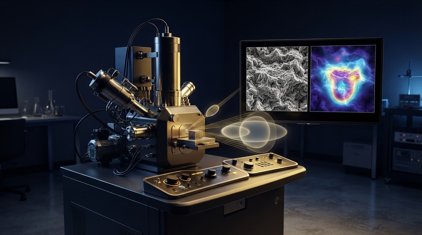
Higher accelerating voltage isn’t automatically better for SEM imaging. If you’re deciding how to choose the right accelerating voltage, start with what you need to learn from the specimen: surface detail, subsurface structure, or elemental composition.
The decision can be challenging because voltage affects several outcomes at once. Higher-energy electrons can penetrate deeper and expand the interaction volume. Lower voltages can increase surface sensitivity and may help limit beam effects on delicate materials. Neither setting guarantees a useful image. Specimen composition, conductivity, preparation, detector choice, and EDS requirements all matter.
This guide explains how lower and higher accelerating voltages affect image contrast, resolution, interaction depth, charging, and sample damage. You’ll find a repeatable way to choose an initial setting for your imaging objective, refine it by comparing results, and decide when to change other conditions or consult instrument-specific guidance. The goal isn’t to find one ideal voltage for every specimen, but to validate a setting that produces useful, reliable data for yours.
Key Takeaways
- Choose voltage according to the information you need from the specimen. Electron penetration and signal generation affect what the SEM reveals.
- To learn how to choose the right accelerating voltage, weigh surface sensitivity against available signal and the requirements of your imaging or EDS objective.
- Don’t assume lowering voltage alone will resolve charging or prevent beam damage. Identify the source of the artifact or specimen change.
- Compare settings systematically. Where feasible, keep other imaging conditions steady, then assess image quality and analytical results.
- If adjustments don’t resolve weak signal, poor contrast, charging, or inconsistent EDS results, review specimen preparation and instrument conditions with qualified application support.
How accelerating voltage changes what an SEM reveals
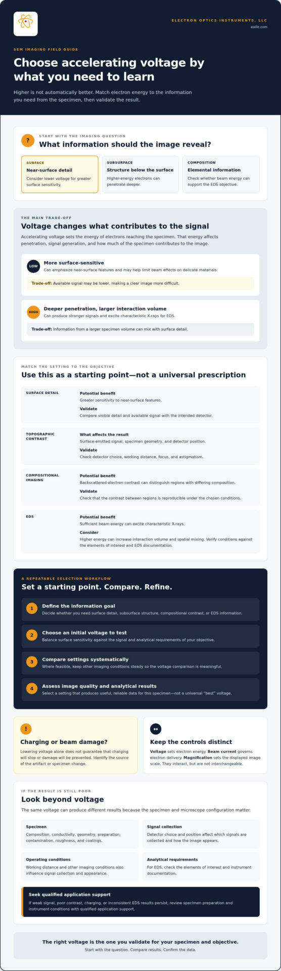
Accelerating voltage sets the energy of the electron beam as it reaches the specimen. It affects how deeply electrons penetrate, which signals are generated, and how much of the specimen contributes to the image. In practice, that means changes to surface sensitivity, contrast, and signal strength, not a simple control for “better” imaging.
In brief: accelerating voltage sets electron energy, beam current governs electron delivery, and magnification sets the displayed scale of the image. These parameters interact, but they aren’t interchangeable. Increasing magnification won’t reveal detail the system hasn’t resolved, and changing voltage alone won’t determine image quality.
What does accelerating voltage mean in SEM?
Electrons gain energy as they accelerate through an electrical potential difference toward the specimen. This potential is commonly reported in kilovolts (kV); electron energy is often expressed in kiloelectronvolts (keV). For foundational background on the electron gun and SEM operation, see the Scanning Electron Microscope (SEM) overview.
Beam current describes the rate of electron delivery to the specimen, while voltage describes the energy of those electrons. Both can affect the signal available for imaging, but in different ways. Resolution and image quality also depend on the electron-optical system, specimen condition, detector, and operating setup.
Why the same voltage can produce different results
A setting that reveals useful surface texture on one specimen may produce a different balance of contrast and signal on another. Material composition affects how electrons scatter and which signals are generated. Geometry matters too: edges, recesses, and sloped features can change how signals escape or reach the detector. Surface contamination, roughness, and coatings can also influence the image.
Detector choice determines which emitted signals are collected. Secondary-electron imaging often emphasizes surface topography, while backscattered-electron imaging can provide compositional contrast. Working distance and detector position also affect signal collection and image appearance. As a result, the same voltage doesn’t guarantee comparable results across different configurations.
For a useful introduction to these interacting components, consult the site’s SEM working-principle guide. When considering how to choose the right accelerating voltage, begin with the imaging question, then account for the specimen, detector, and microscope configuration. Voltage is one part of the decision, not a shortcut to higher resolution.
Match SEM accelerating voltage to the sample and imaging goal
To understand how to choose the right accelerating voltage, identify the information you need before adjusting the setting. Lower voltage can help emphasize near-surface features by limiting electron penetration, but it may also reduce the signal available for a clear image. Higher voltage can produce stronger signals and excite characteristic X-rays for EDS, while probing a larger specimen volume. That larger volume can blend surface detail with information from below it.
Use the comparison below as a starting point, not a set of universal voltage prescriptions. The appropriate setting depends on the specimen, detector, microscope configuration, and analytical objective.
| Objective | Likely benefit | Limitation | Validation step |
|---|---|---|---|
| Surface detail | Greater sensitivity to near-surface features | Lower available signal may make imaging more difficult | Compare detail and signal using the intended detector |
| Topographic contrast | Surface-emitted signal can reveal relief | Detector position and specimen geometry affect contrast | Check detector choice, working distance, focus, and astigmatism |
| Compositional imaging | Backscattered-electron contrast can distinguish regions with differing composition | Contrast also depends on material and imaging conditions | Compare regions and confirm the contrast is reproducible |
| EDS | Sufficient beam energy can excite characteristic X-rays | Higher energy can increase the interaction volume and spatial mixing | Verify conditions against element lines of interest and EDS documentation |
Choosing voltage for surface detail and topographic contrast
For fine surface texture or a thin surface layer, limiting interaction depth may help keep the image focused on near-surface information. Secondary-electron contrast also depends on detector type, detector geometry, and specimen shape, so voltage is only one control. Before attributing a softer or noisier image to voltage, check focus, astigmatism, and signal stability.
Choosing voltage for compositional imaging and EDS
EDS depends on exciting characteristic X-rays, and the relevant ionization thresholds differ by element and X-ray line. JEOL USA describes a practical voltage for elemental analysis guideline of setting beam energy at 1.5 to 2 times the energy of the X-ray lines of interest. Treat this as guidance to verify, not a universal setting. Consult the EDS system documentation and consider the spatial resolution required, since a larger interaction volume can mix signals from neighboring regions.
Set conditions to answer the analytical question, rather than simply maximizing voltage. If you need help evaluating imaging conditions or instrument configuration, consult Electron Optics Instruments, LLC for SEM application support.
Does lower accelerating voltage prevent charging or beam damage?
Reducing accelerating voltage can help with some specimens, but it isn’t a universal remedy for charging or beam-induced change. Charging occurs when electrical charge accumulates because electrons arrive at the surface faster than charge can dissipate. Beam damage, by contrast, is a physical or chemical alteration caused by exposure. Similar image deterioration can have different causes, so changing voltage before identifying the problem may obscure the diagnosis.
Voltage is one control among several, not a standalone fix. Beam current, exposure time, specimen conductivity, grounding, preparation, detector settings, and microscope configuration can all affect the result. Lower voltage may reduce some interactions with the specimen, but it can also weaken the signal or change contrast. The image may look less stable without the underlying issue being resolved.
Diagnosing charging without changing voltage blindly
Charging may appear as image drift, bright patches, streaking, or contrast that shifts during scanning. These signs aren’t conclusive on their own. Contamination, unstable focus, detector response, or other imaging artifacts can also affect brightness and detail. Check whether the effect follows a particular region or appears across the field, and note whether it changes with scan conditions.
Depending on the specimen and instrument, possible approaches include improving electrical contact to the stub, applying a suitable conductive coating, or using low-vacuum operation. Beam current may also be adjusted where the microscope’s operating procedures allow. Follow specimen-preparation and instrument protocols, and change one parameter at a time so you can identify which adjustment improves the image.
Protecting beam-sensitive or delicate specimens
Beam exposure can contribute to contamination buildup, shrinkage, heating, or loss of fine structure in sensitive materials. These changes may develop during observation, so a sharp initial image doesn’t establish that the chosen conditions are harmless. Lower voltage alone can’t guarantee that a specimen will remain unchanged.
Limit exposure where practical. Focus and adjust the image on a representative area rather than repeatedly scanning the feature you need to preserve, and test conditions on a comparable region before prolonged imaging. If fine detail shifts, fades, or appears altered over successive scans, reduce exposure and review other available controls, such as beam current or scan strategy, in accordance with instrument guidance.
In practice, how to choose the right accelerating voltage also means checking whether an apparent improvement is genuine. Compare images under controlled conditions, distinguish charging from specimen alteration or detector-related artifacts, and record the settings that produced the result. If the cause remains unclear, seek qualified application guidance before making further changes.
How to test and refine accelerating voltage systematically
A controlled comparison helps separate the effect of accelerating voltage from changes caused by other imaging conditions. Define what a successful result must show, then assess whether each test improves the information you need without introducing unacceptable artifacts or specimen changes.
Keep the same field, detector, working distance, and beam-current strategy where feasible. If another parameter must change to obtain a usable image, record it so you can distinguish the effect of voltage from the effect of that adjustment.
Run a controlled voltage comparison
Begin with a baseline recommended by the microscope documentation or your lab’s procedure. Make measured voltage adjustments within the instrument’s approved operating conditions, allowing the image to stabilize after each change. Keep the specimen position and other relevant settings consistent, and capture comparable images of the same field when practical.
Use this sequence to guide the test:
- 1. Define the objective. Specify the feature, contrast, or analytical signal you need to resolve.
- 2. Stabilize the setup. Set the detector, working distance, beam-current approach, focus, and other conditions before comparing voltage.
- 3. Compare settings. Change voltage in measured increments and save an image at each condition.
- 4. Assess the result. Check target-feature visibility, useful signal, charging, possible specimen damage, and analytical needs. Don’t treat a brighter image as automatically better.
- 5. Select and verify. Choose the condition that best serves the objective, then repeat or confirm it to check for consistency.
Record settings so results are reproducible
Document the accelerating voltage alongside specimen and imaging conditions. Voltage alone isn’t enough to reproduce an SEM result. Record beam current, detector, working distance, vacuum mode, specimen preparation, and the location imaged. Note charging, contamination, apparent beam damage, and any changes in image interpretation. These observations can help explain why a setting worked or why it didn’t transfer to another specimen.
For further guidance, review the microscope manufacturer’s recommendations and your lab’s established SEM imaging procedures.
If you need help evaluating test results or developing a repeatable workflow, discuss your SEM application with Electron Optics Instruments, LLC.
When to seek SEM application support for voltage selection
If systematic comparisons still leave you with weak signal, persistent charging, poor contrast, or inconsistent EDS results, the next step may not be another voltage adjustment. These problems can arise from specimen preparation, instrument configuration, detector selection, analytical requirements, or a combination of factors. Qualified support can help review the full imaging workflow and determine which variables to investigate.
Before asking for guidance, record the specimen, imaging objective, settings tested, and observed changes. A concise history helps distinguish a reproducible application challenge from an isolated image artifact and avoids premature conclusions about instrument performance.
Signs that the issue may extend beyond voltage
Review preparation and operating conditions, including electrical contact, contamination, focus, astigmatism, vacuum conditions, and detector choice. If instability continues across fields or persists under conditions that previously produced consistent results, document when the change began and what has already been checked. Image symptoms alone aren’t enough to diagnose an equipment fault, so avoid making instrument adjustments outside established procedures.
Connect voltage decisions to the right SEM setup
Voltage is one part of matching an SEM to the lab’s work. Consider specimen types, the image information you need, throughput needs, and whether the workflow also requires EDS. The appropriate instrument configuration depends on those priorities and should be checked against current manufacturer documentation. The Cube II Benchtop SEM is one of Electron Optics Instruments, LLC’s offerings, but verify product specifications for the intended application.
Application guidance can also help a lab turn a successful setting into a repeatable operating practice. Electron Optics Instruments, LLC provides SEM training and service for microscopes from multiple manufacturers, which may be relevant when operators need help reviewing workflows or imaging conditions. If you’re still evaluating how to choose the right accelerating voltage, bring your test observations and application requirements to a qualified technical contact.
Discuss your SEM application needs with Electron Optics Instruments, LLC to identify what information may help guide the next step.
Build a Repeatable SEM Imaging Approach
The right accelerating voltage depends on what you need to learn from the specimen, not on a universal setting. Lower voltage may bring near-surface features into focus, while higher voltage can support deeper interaction and EDS analysis, with trade-offs in signal and detail. To determine how to choose the right accelerating voltage, define your imaging objective, compare settings under controlled conditions, and assess more than brightness. Consider feature visibility, charging, specimen changes, and analytical needs.
Record voltage alongside detector, working distance, beam current, specimen preparation, and other relevant conditions. That documentation helps you reproduce useful results and identify when the challenge may extend beyond voltage selection.
Electron Optics Instruments, LLC provides SEM training, maintenance, and repair support. If you need help reviewing imaging conditions or building a repeatable workflow, discuss your SEM application with Electron Optics Instruments, LLC. A disciplined comparison and qualified guidance can help your lab make more informed imaging decisions.
Frequently Asked Questions
What is the best accelerating voltage for SEM imaging?
There isn’t one best accelerating voltage for every specimen or imaging objective. To determine how to choose the right accelerating voltage, weigh the need for surface sensitivity against available signal, and consider material composition, detector choice, and whether analysis such as EDS is required. Start with guidance for your specific instrument, then compare settings under controlled conditions using the feature or signal you need to evaluate.
Is lower accelerating voltage always better for high-resolution SEM images?
No. Lower voltage can increase surface sensitivity in some applications, but it doesn’t guarantee higher resolution or a clearer image. Signal strength, probe conditions, detector, working distance, specimen properties, and image stability also matter. Where feasible, compare settings while keeping other imaging conditions consistent. Judge whether the detail you need is genuinely more visible rather than assuming lower is always better.
Can accelerating voltage reduce charging in an SEM?
Lowering voltage may reduce charging in some situations, but it isn’t a guaranteed solution. Charging also depends on specimen conductivity, grounding, coating, vacuum mode, beam current, and sample preparation. Look for symptoms such as drift, bright patches, streaking, or unstable contrast, while considering other sources of image artifacts. Test suitable adjustments systematically, changing one condition at a time where practical, and follow the instrument’s operating guidance and laboratory procedures.
How does accelerating voltage affect EDS analysis?
Accelerating voltage affects whether the beam can excite characteristic X-rays from the elements of interest, as well as the specimen volume contributing to the spectrum. The appropriate setting depends on the target elements, specimen composition, and EDS system guidance. Consult the application documentation to confirm suitable operating conditions. Balance the excitation needed for reliable analysis against spatial-resolution goals, since signals from a larger interaction volume may include material beyond the specific feature being examined.
What happens if SEM accelerating voltage is too high?
Higher voltage can increase electron penetration and expand the signal-generating volume, which may reduce surface specificity or affect a sensitive specimen. That doesn’t make a high setting inherently wrong. It may suit a particular imaging or analytical objective. Assess whether the image answers the intended question, monitor the specimen for changes, and consider EDS requirements before adjusting. If surface detail is being obscured, compare a lower setting under controlled conditions.
Should accelerating voltage be changed together with beam current?
Usually, change one variable at a time where practical. Voltage sets electron energy, while beam current relates to electron delivery. Both can affect available signal and specimen response. Adjusting both simultaneously makes it difficult to identify which change improved or degraded the image. Hold beam current steady during a voltage comparison when feasible, then evaluate current separately if needed. Record both values, along with detector and working distance, so the result can be reproduced.