
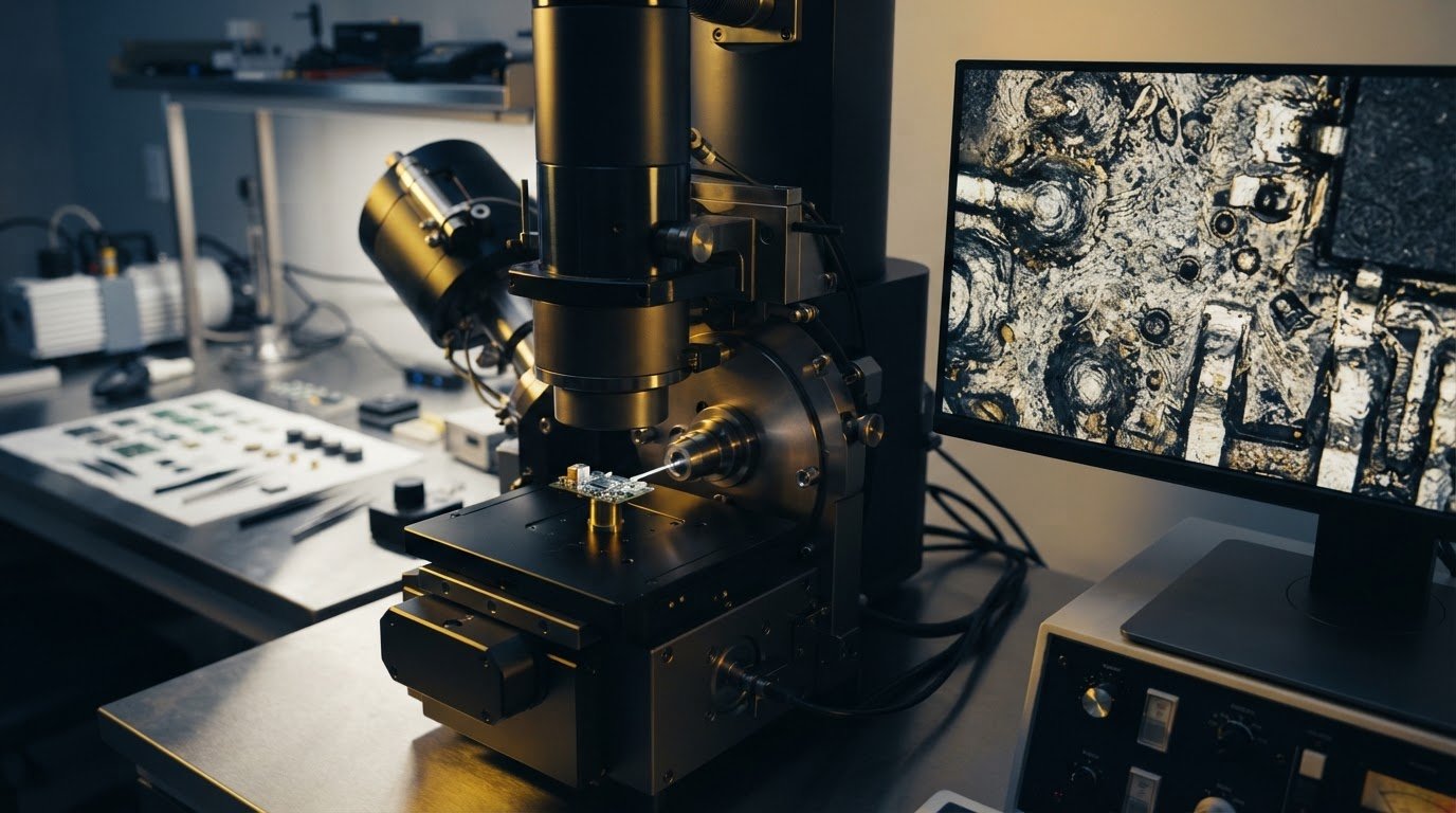
Quality assurance in electronics manufacturing with SEM imaging helps teams examine component surfaces and material features beyond the reach of conventional visual inspection. Scanning electron microscopy can support checks for physical defects and material differences, while energy-dispersive spectroscopy (EDS) can provide elemental composition data. These findings inform component evaluation and failure analysis, but complement rather than replace electrical and other production tests.
Reliable electronics depend on more than a successful final test. Inspection findings are most useful when linked to component records, production stages, and documented acceptance criteria. This helps teams investigate deviations and assess whether corrective actions address the underlying cause.
This article explains how SEM fits into a broader quality assurance system, from component checks and traceability to process validation and root-cause analysis. You’ll learn what SEM can reveal, where its limits matter, and how manufacturers can use its evidence alongside other inspection and testing methods to make better-informed production decisions.
Key Takeaways
- Use SEM imaging to examine surface features and material differences that can inform component evaluations and failure investigations.
- Connect inspection findings with component and production records to make deviations easier to trace and assess.
- Pair SEM evidence with process data and repeatable test methods to investigate non-conformities and validate corrective actions.
- Choose inspection methods according to the feature being examined: SEM, optical microscopy, X-ray inspection, and EDS provide different kinds of evidence.
Root-cause analysis and process validation
SEM findings can help teams investigate physical irregularities alongside production and test records. Their value increases when manufacturers connect inspection evidence to process decisions and documented quality controls.
Root-Cause Analysis
Root-cause analysis investigates a non-conformity to identify the process condition that produced it. To validate a process, teams compare SEM observations with work instructions, material records, and acceptance criteria. A surface anomaly can prompt a review of the affected lot, supplier documentation, and production stage. Teams can then test a corrective action and inspect subsequent results for recurrence. This links physical evidence to an evaluated change instead of treating each error as an isolated event. If the adjustment reduces repeat findings, that supports the conclusion that the relevant process control is working as intended.
Using Test Results for Process Improvement
Test results guide process improvement by showing where performance changes across production checkpoints. Statistical process control helps teams identify recurring trends rather than react to a single result. Custom fixtures and automated test stations can apply repeatable checks at different manufacturing stages. Teams can compare those results with SEM observations to distinguish a material issue from a process-related pattern. When evidence points to a non-conformity, corrective actions may include process adjustments, rework, supplier notification, or design changes. Recording the action and subsequent inspection results helps determine whether the change addressed the underlying cause. When rejected assemblies or retired test hardware cannot be salvaged through rework, organizations such as the Electronic Recycling Association (ERA) provide responsible electronics recycling and collection options.
Manufacturing Process Consistency
Manufacturing process consistency means applying documented methods and acceptance criteria across production runs. Consistency makes lot-to-lot quality control more meaningful and supports confidence in supplier performance across orders. Employee training reinforces consistent practice when it covers product specifications, inspection techniques, testing procedures, and quality assurance principles. For example, operators using the same inspection criteria can record comparable findings at each production stage. Managers can review defect rates, customer complaints, and delivery performance alongside process data. These measures help identify where instructions, equipment settings, or training need adjustment to reduce recurring errors and strengthen compliance.
Component presence, placement, orientation, and identification checks
SEM supports detailed examination of selected components, but it is not a complete production inspection system. It shows surface features and fine physical detail, but cannot alone confirm electrical function, hidden solder joints, or component authenticity. Use SEM alongside in-circuit testing, records, and other suitable inspection methods.
For a populated circuit board, inspection criteria can cover whether a component is present, correctly positioned, oriented to its design specification, and visibly intact. SEM imaging can examine selected features, such as a package surface or suspected physical defect. Routine production checks still require methods suited to the full assembly and inspection rate. In-circuit testing can identify shorts between PCB nets, opens, incorrect values, missing parts, and some solder-related defects. These results can help distinguish electrical problems from visible surface conditions.
Traceability connects component and assembly records from incoming materials through finished products. Link inspection and test results to component identification, supplier documentation, lot, and production stage. Sourcing from reputable suppliers such as Adage Components provides the reliable documentation and batch consistency that manufacturing teams need for traceability. These records help teams investigate whether a defect appears across a particular lot or process point, and support informed procurement decisions if availability changes. Production data is more useful when teams can compare findings across orders rather than treat each result as an isolated event.
For selected component examinations, SEM inspection equipment can support closer analysis of physical features. The value comes from aligning each inspection with its purpose: use SEM for detailed surface evidence, in-circuit testing for electrical defects, and traceability records to connect findings with components and production history.

Quality assurance in electronic manufacturing
Electronics quality assurance uses defined requirements, inspection methods, and production controls to verify products at relevant stages. Quality assurance in electronics manufacturing with SEM integrates imaging evidence into these controls without treating microscopy as a substitute for functional testing. Specifications establish dimensions, materials, tolerances, and functional requirements. Incoming inspection can assess a printed circuit board lot against material and dimensional criteria before assembly. Continuous monitoring adds process data, helping teams detect changes before they affect more products. SEM can provide detailed physical evidence when a feature needs closer examination.
IPC standards address electronic design, assembly, and testing. IPC-A-610 covers acceptability of electronic assemblies; IPC-A-600 and IPC-6012 address printed circuit board acceptance and performance requirements. IPC-J-STD-001 covers soldered electrical and electronic assemblies, while IPC-TM-650 provides test methods, including Dye-and-Pry examination of BGA solder joints. ISO 9001 supports general quality management. Industry-specific frameworks include IATF 16949 for automotive, AS9100 for aerospace, and ISO 13485 for medical devices. The applicable criteria depend on product type, customer requirements, and the process being evaluated.
Standards provide shared criteria, which manufacturers translate into controlled work instructions and records. An inspection plan defines what teams examine, which method they use, and how they document results. Automated optical inspection can assess assemblies at multiple SMT stages, while electrical testing identifies functional defects that images may not reveal. For safety-critical applications, 100% testing is often mandatory to meet regulatory compliance. End-of-line checks may combine functional, performance, and reliability tests based on product requirements. In quality assurance in electronics manufacturing with SEM, teams can use defect trends and inspection evidence to guide investigation, while documented corrective actions help prevent recurring issues that may contribute to recalls.
How does SEM compare with optical microscopy, X-ray inspection, and EDS for quality control?
Each method answers a different inspection question. Optical microscopy, scanning electron microscopy (SEM), X-ray inspection, and energy-dispersive spectroscopy (EDS) provide complementary evidence. The right choice depends on whether teams need to examine surface detail, internal structure, or elemental composition.
Optical microscopy uses visible light to examine features such as solder fillets, component alignment, and surface damage. It supports visual checks across accessible areas of a board, but provides less image detail than SEM. SEM scans a sample with an electron beam, revealing fine surface topography, cracks, residues, or package features that may be difficult to characterize optically. For example, teams investigating a surface defect can use SEM images to assess its shape and location.
X-ray inspection provides a different view: it can reveal hidden or hard-to-see solder joints, including connections beneath ball grid array (BGA) packages. This is useful when a board’s top surface appears acceptable but internal joints remain inaccessible to direct visual inspection. SEM examines exposed surfaces and does not replace X-ray assessment of concealed connections. Choose the method according to the inspection question.
EDS is commonly paired with SEM to analyze the elements present in a selected area. If a deposit or inclusion appears on a component, SEM imaging shows its physical form, while EDS can provide elemental composition data to inform the investigation. This supports material comparison, but EDS results should be interpreted alongside sample context and other quality records, not treated as a complete diagnosis on their own.
Choose the method by matching the suspected defect to the evidence required: optical microscopy for accessible visual features, X-ray for hidden joints, SEM for detailed surface morphology, and EDS for elemental analysis. For a closer look at SEM options for component analysis, explore SEM systems.
Electron Optics Instruments: Cube II Benchtop SEM
Electron Optics Instruments, LLC offers the Cube II Benchtop SEM for teams seeking equipment to support component examination and quality investigations. Use SEM when a suspected surface defect, material feature, or component anomaly requires closer imaging than routine visual inspection can provide. These observations can inform analysis alongside electrical tests, production records, and other inspection methods suited to the suspected issue. The company also offers the Genesis Tabletop SEM and Veritas Series SEM for manufacturing and research applications. Choose an instrument by defining the sample, the feature to examine, and how the findings will support quality decisions. Contact Electron Optics Instruments, LLC to discuss SEM equipment for your inspection needs.
Turn Inspection Questions into a Clear Evaluation Plan
Start with a clearly defined inspection objective: identify the sample, the feature requiring examination, and the decision the results must support. This focus helps determine whether SEM imaging belongs in the evaluation and what complementary evidence the quality team needs. Quality assurance in electronics manufacturing with SEM is most useful when observations address a specific engineering question, rather than becoming images without a defined role in decision-making.
For teams assessing SEM equipment, Electron Optics Instruments offers the Cube II Benchtop SEM, Genesis Tabletop SEM, and Veritas Series SEM. The right instrument depends on the samples and inspection objectives your manufacturing process requires. Use those criteria to shape a practical equipment discussion and align the evaluation with your quality workflow. Contact Electron Optics Instruments to discuss SEM equipment for your application, and take the next step toward a more deliberate inspection strategy.
Frequently Asked Questions
How is scanning electron microscopy used to inspect electronic components and circuit boards?
Scanning electron microscopy examines selected component or board features by scanning the sample with an electron beam. In quality assurance in electronics manufacturing with SEM, an engineer may compare a damaged connector surface with an unaffected area or inspect a bond wire in greater detail. The resulting image helps characterize physical structure and surface condition. It does not establish whether the circuit operates correctly, so electrical measurements remain important.
What defects can SEM detect in solder joints, PCB traces, and semiconductor devices?
SEM can reveal surface features such as cracks, corrosion, residue, roughness, and physical damage on accessible areas. On an exposed solder joint, it can help characterize surface cracking; on a PCB trace, it may show edge damage or discontinuities. Semiconductor inspection can reveal surface particles or layer irregularities. Internal defects require suitable exposure or another method, and image findings alone do not confirm electrical failure.
What are the steps for SEM failure analysis in electronics manufacturing?
Start by defining the failure symptom and preserving the sample’s condition and production history. Select the area most likely to distinguish competing explanations, then image it and compare affected and unaffected regions. If elemental composition could clarify a deposit, pair imaging with EDS. A quality assurance in electronics manufacturing with SEM workflow then correlates these observations with electrical results and process records before documenting a likely cause and evaluating corrective action.
What SEM sample preparation methods are used for electronics inspection?
Preparation depends on the sample’s material, geometry, and inspection objective. A small component may be secured to a sample mount, while a board section may need cutting to expose the feature of interest. Keep the sample clean and firmly held; nonconductive materials may require a conductive coating to reduce charging. Preserve the defect location during preparation, since cutting or handling can alter fragile surfaces and complicate interpretation.