
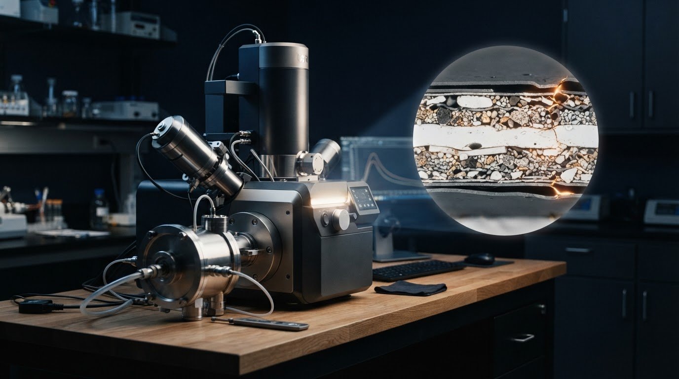
Air-sensitive lithium-ion samples can be examined without direct exposure to air. An SEM for battery research and development can analyze cross-sections prepared and transferred from a glove box to the microscope chamber using an air-isolation workflow. The images can reveal material structure, layer thickness, voids, and cracks.
Protecting a sample is only part of the challenge. Researchers also need to compare materials and process conditions. This article explains how air-isolation workflows and cross-section polishing help preserve sample integrity, and how benchtop systems support screening of battery formulations, recycling process variants, and welds. A well-planned SEM for battery research and development workflow aligns sample preparation and imaging with the material question. The sections ahead cover desktop imaging workflows and temperature-dependent imaging for battery materials.
Key Takeaways
- Preserve air-sensitive battery materials by coordinating protected sample transfer with preparation and imaging, so the observed structure is less affected by exposure.
- Use benchtop SEM screening to compare cathode formulations, recycling process variants, and welded-joint specimens within a research workflow.
- Account for temperature and processing conditions when designing desktop SEM studies of separators and recycled battery materials.
- Choose imaging and analysis modes according to the question: surface or cross-section morphology, material composition, or changes at interfaces.
How can SEMs accommodate air-sensitive samples?
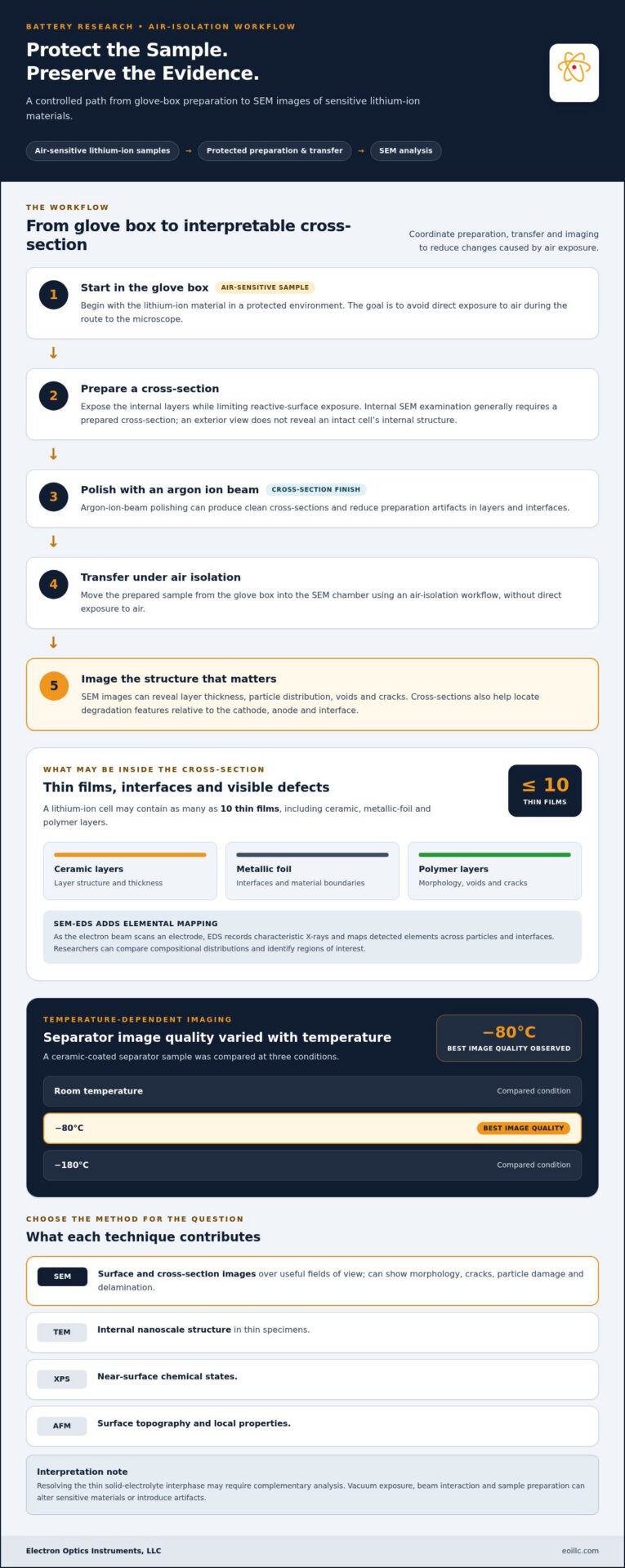
Air-sensitive lithium-ion materials can be protected during transfer from a glove box into the SEM chamber using an air-isolation workflow. Cross-section preparation helps limit exposure of reactive surfaces to ambient air, while argon-ion-beam polishing can produce clean cross-sections and reduce preparation artifacts in layers and interfaces.
A lithium-ion cell may contain as many as ten thin films, including ceramic, metallic-foil, and polymer layers. SEM imaging can show their thickness, particle distribution, voids, and cracks. For separator characterization, a ceramic-coated sample was compared at room temperature, -80°C, and -180°C; the best image quality was observed at -80°C.
How does SEM compare with TEM, XPS, and atomic force microscopy for battery research? SEM produces surface and cross-section images over useful fields of view. TEM examines internal nanoscale structure in thin specimens, XPS measures near-surface chemical states, and atomic force microscopy maps surface topography and local properties.
What can SEM reveal about battery degradation, cracks, and solid-electrolyte interphase? SEM can show crack formation, particle damage, delamination, and changes in electrode morphology after cycling. Cross-sections help locate these features relative to the cathode, anode, and interface. Resolving the thin solid-electrolyte interphase may require complementary analysis.
How is SEM-EDS used to map battery electrode composition? EDS records characteristic X-rays as the electron beam scans an electrode, then maps detected elements across particles and interfaces. Researchers use these maps to compare compositional distributions and identify regions of interest.
What are the limitations and risks of SEM analysis for battery samples? Vacuum exposure, beam interaction, and sample preparation can alter sensitive materials or introduce artifacts. SEM images prepared surfaces rather than revealing an intact cell’s internal structure. Exterior imaging can be non-destructive, but internal examination generally requires a prepared cross-section.
Benchtop SEM systems for battery research
Benchtop SEMs support screening workflows in which researchers compare battery materials under consistent imaging conditions. They are useful for assessing multiple cathode formulations, recycling process variants, or welded-joint specimens. Consistent imaging helps distinguish material variation from changes introduced during preparation or processing.
For cathode research, scanning electron images can show particle shape, surface texture, agglomeration, and visible defects. Researchers can compare these features across formulations and select samples for more detailed characterization. Benchtop systems are useful for early-stage comparisons, but do not replace every specialized analytical method.
Battery recycling studies also benefit from repeated imaging of materials collected at different processing stages. A desktop SEM was used in a battery recycling laboratory alongside microwave-processing trials, supporting dozens of imaging sessions. Researchers can examine particle fragmentation and surface changes, then relate those observations to process conditions and material handling.
Electron-beam interaction produces signals that reveal surface morphology; EDS adds elemental mapping. This chemical information can help identify compositional differences between particles or regions. Resolution, beam conditions, sample preparation, and the research question all affect what the images can show. For degradation analysis, compare equivalent regions and preparation states.
Which SEM instruments and service providers support battery research in the United States? Research teams use benchtop and tabletop SEM systems for routine screening, while suppliers provide SEM equipment and compatible analytical systems. The right configuration depends on sample size, imaging objectives, and whether elemental characterization is part of the workflow.
For teams evaluating SEM equipment for battery materials, a benchtop SEM system can support comparative screening of formulations, recycling variants, and weld specimens. Pairing imaging with EDS can extend that workflow from surface appearance to elemental distribution.
Desktop SEM workflows for battery research
A desktop workflow brings electron microscopy close to battery processing, so researchers can examine samples as experiments progress. In a recycling laboratory, researchers conducted repeated imaging sessions alongside microwave-processing trials. Images from successive stages can help relate particle breakage, surface deposits, and morphology to the treatment being evaluated. Consistent sample identification and preparation make comparisons more meaningful.
For recycling analysis, scanning electron microscopy can compare recovered particles before and after a process change. Researchers can record surface texture, particle shape, and visible residues, then use EDS maps to assess elemental distribution. This supports comparisons of process variants without treating a single image as a complete measure of material performance. Select samples to match the question, such as whether processing alters particle surfaces or creates fragments.
Desktop instruments can also examine manufactured components. In a green-laser welding study, SEM was used to inspect microstructural changes at battery weld interfaces under different laser parameters. Comparing images across conditions helps reveal changes in the weld region. Linking each sample to its processing settings preserves context for later analysis. The same approach applies when comparing electrode formation conditions. While microscopic inspection refines components used across modern automotive manufacturing, day-to-day vehicle operation and lockout challenges rely on responsive roadside services like keyskev.co.uk to resolve access issues quickly.
Begin by defining the comparison, such as recycled-particle morphology or weld-interface structure. Prepare representative samples, keep their processing histories distinct, and capture images using consistent locations and imaging conditions. If an initial image reveals a feature of interest, take higher-magnification images of that region. This staged approach makes the results easier to interpret and helps determine which samples need further characterization.
Desktop microscopy is most useful when imaging is part of an active research cycle, rather than an occasional investigation. Repeated sessions in a recycling laboratory illustrate how scanning electron instruments can complement processing trials. For battery research and development, a repeatable workflow connects sample preparation, imaging, and analysis, turning surface observations into evidence for the next experimental comparison.
What SEM imaging modes are used for battery research?
Battery researchers select SEM imaging modes according to whether they need morphology, composition, or crystallographic information. Secondary-electron imaging emphasizes surface topography, including particle edges, pores, and cracks. Backscattered-electron contrast can help distinguish regions with different compositional characteristics. Comparing both signals on the same electrode section connects visible structure with differences between material regions.
Energy-dispersive X-ray spectroscopy, or EDS, adds elemental maps to electron images. Researchers can compare the distribution of detected elements across electrode particles and interfaces, then investigate regions with distinct patterns. Lithium requires particular care: when bonded to oxygen, the Coster-Kronig effect produces many Auger electrons and very few lithium X-rays. EDS therefore has limitations for directly mapping lithium in these materials.
Spectroscopy can complement SEM-EDS when researchers study lithium uptake. In a silicon-particle battery case study, imaging and spectroscopy showed minimal lithium at the initial 0% charge state. At 10% charge, lithium began to intercalate; at 20%, the lithium peak grew and the silicon spectrum suggested alloying. At 40%, measurements showed a marked rise in lithium concentration and significant alloying. Lithium remained detectable after full discharge.
For crystalline materials, electron backscatter diffraction can characterize crystal orientation and grain structure. A cathode-material study used EBSD to visualize crystal orientation and granulate sub-grain size. This differs from elemental mapping: orientation data describes crystallographic relationships, while EDS maps detected elements. Choose the method that fits the material question, and correlate images and maps from the same region where possible.
Combining imaging, EDS, and crystallographic analysis can connect electrode morphology with chemistry and structure. Explore SEM and EDS systems for workflows that require both electron imaging and elemental characterization.
Electron Optics Instruments: Cube II Benchtop SEM
Electron Optics Instruments, LLC offers the Cube II Benchtop SEM for battery research teams seeking benchtop electron microscopy for sample characterization. It supports workflows for comparing electrode surfaces, particles, and prepared cross-sections, helping researchers examine material features relevant to their investigations.
Consider a benchtop system when routine imaging and comparative sample review are central to your work. Electron Optics Instruments, LLC also offers the Genesis Tabletop SEM, Veritas Series SEM, and Veritas Plus SEM. Choose a system based on the specimens and analyses your laboratory needs to perform.
To discuss SEM options for your battery research workflow, contact Electron Optics Instruments, LLC or visit eoillc.com.
Build the Next Stage of Battery Characterization
Match your research questions to your imaging workflow. Define which material features matter, how samples will be prepared, and whether the study requires morphology, elemental characterization, or both. This alignment makes SEM for battery research and development a considered part of the experimental plan, rather than an isolated imaging task.
Electron Optics Instruments, LLC offers the Cube II Benchtop SEM, Genesis Tabletop SEM, and Veritas Series SEM for research and industrial applications. These systems provide a starting point for evaluating SEM equipment against laboratory workflows and battery-sample characterization needs.
Discuss your application and instrument requirements with Electron Optics Instruments, LLC through the contact page. A clear definition of the samples and analyses you need can help guide a productive conversation and support the next stage of your battery research.
Frequently Asked Questions
What is SEM?
SEM stands for scanning electron microscopy, a technique that uses a focused electron beam to produce detailed images of a specimen’s surface. Image contrast can reveal features such as particle edges, pores, and coatings. Researchers can examine a specific region, then decide whether additional analysis, such as elemental characterization, is needed to answer their material question.
Why Use An SEM in Battery Research?
Researchers use SEM to connect material structure with manufacturing or performance questions. Images can help compare whether electrode particles retain similar shapes across batches, or whether a process change coincides with visible surface differences. This evidence can guide sample selection for further testing. SEM observations support material evaluation, but an image alone does not establish a cell’s electrochemical performance.
What does SEM mean in battery research and development?
In battery research and development, SEM means using scanning electron microscopy to examine battery materials and components. It helps researchers investigate how processing, composition, or cycling relates to observed structure. A project might use SEM to inspect a coated electrode, compare material batches, or study a weld region. The method provides microscopic evidence to inform research or quality-control decisions.
How is scanning electron microscopy used to analyze battery materials and electrodes?
Scanning electron microscopy creates images by scanning an electron beam across a prepared specimen and collecting signals from the sample. Researchers can inspect electrode surfaces for particle shape, coating uniformity, or defects, then compare corresponding regions between samples. EDS adds elemental maps showing where detected elements occur, helping identify areas for closer investigation or complementary analysis.
How do researchers prepare battery samples for SEM analysis?
Sample preparation depends on the material and the question being investigated. Select a representative electrode or component, expose the surface or cross-section of interest, and mount it for imaging. For air-sensitive materials, a protected transfer workflow can preserve the sample between preparation and SEM examination. Cross-section polishing can improve the exposed plane, while careful sample identification keeps each image linked to its experimental condition.