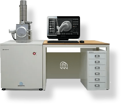
The scanning electron microscope, or SEM for short, was a pivotal breakthrough in the fields of microscopy and high-resolution imaging. Researchers were finally able to overcome the optical resolving limits of visible light and observe the microstructural properties of objects at unprecedented scales. Consequently, SEM technology was the only way to visualize the detailed microstructural characteristics of bulk objects with high resolutions.
The Benefits of SEM Technology
Conventional imaging systems, such as the compound microscope, offer resolutions approaching 5 nanometers (nm), which translates to magnification ranges of up to 1,000x. SEM technology exceeds that by several orders of magnitude. Magnifications of 30,000 – 200,000x are routine with scanning electron microscopy. This is coupled with the technology’s large depth of field, yielding three-dimensional SEM images with outstanding optical resolution.
So, how do SEM microscopes work?
Working Principles of SEMs
SEM technology uses a finely focused electron beam to raster scan samples and irradiate the surface. This is generated using an electron optical column which comprises several key components. These can include:
- An electron gun, which provides a stable source of electrons.
- Beam alignment coils, which position the beam in the center of the optical column.
- Condenser and final lens, which form a de-magnified image of the high-power electron beam crossover to form the final probe which is focused into a spot on the sample.
- Scanning coils, which deflect the beam continuously in the X plane and slightly in the Y plane to form a raster scanning pattern
- Stigmator coils, which apply a weak correcting magnetic field to correct losses of symmetry.
Several signals are produced when the beam impinges on the surface: backscattered electrons (BSEs) and secondary electrons, as well as backscattered X-rays. Detectors positioned in the sample chamber obtain these characteristic signals to create a detailed image of the sample’s topographical features.
Though BSEs and X-rays can offer detailed insights into sample composition and other properties, secondary electrons are perhaps most important for generating high contrast SEM images. This is because their emission is largely confined to the volume nearest to the beam impact zone.
Applications of SEM Technology
The applications of SEM microscopy are practically limitless. By providing high-resolution 3D surface maps of various bulk solids at the sub-micro range, SEM technology has become a staple of academic and research laboratories around the world. At Electron Optics Instruments, we routinely supply high-performance scanning electron microscopes to researchers in materials science spaces, helping with the innovative drive towards functional nanotechnologies and novel nanoscale systems like carbon nanotubes.
With unprecedented spatial resolution, SEM systems have also proven essential in quality assurance and control (QA/QC) processes for high-density electronics and advanced semiconductors.
Beyond the commercial and manufacturing sectors, SEM is also empowering scientists in forensic labs, providing the means for next-generation forensic insights. Analysts can now examine myriad materials at high and low magnifications without compromising their depth of focus, offering unmatched data capture for an array of forensic sciences. This same level of power and precision extends into the medical sector too.
This is merely a selection of the applications suitable for SEM technology. If you would like to discuss the possibility of leveraging a scanning electron microscope for your needs, simply contact a member of the EOI team today.