By 2026, the threshold for industrial excellence no longer rests at the micrometer scale; it demands a sub-0.5 nanometer precision that traditional imaging protocols can’t sustain. You recognize that characterizing next-generation nanomaterials requires more than just high magnification, yet the persistent frustration of charging effects on non-conductive samples or the data silos between topographical imaging and elemental mapping often stalls critical failure analysis. It’s a challenge that demands a shift from standard observation to a more integrated, evolutionary approach to microscopy. Precision is no longer optional.
This guide empowers you to master advanced sem techniques that bridge these gaps, ensuring your laboratory achieves the rigorous standards required for modern semiconductor and aerospace engineering. We’ll examine the seamless integration of EDS and EBSD modalities alongside low-vacuum innovations that transform how we visualize sensitive substrates, providing a comprehensive roadmap for optimizing your analytical workflow.
Key Takeaways
- Understand the evolutionary transition from traditional surface imaging to multi-dimensional characterization, reflecting the shift toward comprehensive material intelligence in industrial research.
- Analyze the mechanics of Field Emission sources and integrated STEM capabilities to achieve the sub-nanometer precision required for modern high-resolution imaging.
- Master the integration of EDS, EBSD, and EELS to facilitate a synergistic analytical approach that defines the current standard for advanced sem techniques.
- Identify specialized modalities such as Environmental and Cryo-SEM to overcome the technical challenges associated with non-conductive materials and biological specimens.
- Optimize laboratory productivity by implementing structured workflows and technical training protocols that ensure the maximum return on high-performance optical investments.
The Evolution of Advanced SEM Techniques in Industrial Research
The trajectory of industrial microscopy has moved beyond simple visual inspection toward a holistic, multi-dimensional characterization of matter. For decades, the Scanning electron microscope remained a specialized asset confined to large-scale floor models within elite academic institutions. By 2024, the global market witnessed a 15% increase in the deployment of compact, high-performance systems that decentralized this capability across manufacturing hubs. As we enter 2026, advanced sem techniques represent the integration of high-resolution optics with real-time digital processing. This evolutionary shift isn’t just about magnification; it’s about the precision required to validate sub-5nm semiconductor nodes and complex aerospace alloys. Modern systems now function as integrated analytical laboratories where digital synchronization ensures that every electron interaction provides actionable intelligence for material scientists.
The 2026 landscape demands a level of throughput that was previously unattainable. Industrial competition relies on the ability to move from sample preparation to data visualization in minutes rather than hours. This requirement has forced a transition from manual, operator-dependent workflows to automated, software-driven environments. Digital integration allows for the seamless overlay of multiple datasets, creating a comprehensive map of material properties. This connectivity is essential for maintaining the rigorous standards of global supply chain excellence and sustainable innovation. It ensures that the transition from laboratory prototypes to mass production remains seamless and technically sound.
From Topography to Analytical Depth
Traditional secondary electron imaging often fails to capture the intricate chemical gradients required for 2026 battery technology standards. Modern protocols move beyond surface topography to extract structural, chemical, and crystallographic data in a single session. This multi-modal approach relies on the simultaneous acquisition of backscattered electrons and characteristic X-rays. Achieving a signal-to-noise ratio improvement of 25% or higher is now a standard benchmark. It allows researchers to distinguish between phases that were previously indistinguishable. This depth of characterization is vital for maintaining competitive advantages in material science, ensuring that internal structures meet the precise engineering tolerances of the automotive and electronics sectors.
The Role of Precision Optics in 2026
The excellence of 2026 microscopy stems from radical advancements in electromagnetic lens design. These configurations provide unprecedented beam stability, even during 24-hour automated cycles. Automated alignment algorithms have reduced operator-induced variance by nearly 40% since 2022, ensuring that data remains consistent across different shifts and locations. High-brightness sources, such as cold-field emission guns, deliver superior image clarity at magnifications exceeding 1,000,000x. These optical solutions ensure that advanced sem techniques remain reliable under the rigorous demands of industrial research. Precision in beam steering and spot size control facilitates the rapid throughput necessary for high-volume quality assurance in a global manufacturing context.
High-Resolution Imaging Modalities: FE-SEM and STEM
Field Emission SEM (FE-SEM) Performance
FE-SEM performance excels in the low-voltage regime, specifically between 0.1 kV and 5 kV. This capability is critical for imaging beam-sensitive materials such as photoresists or non-conductive ceramics without the need for heavy conductive coatings. While traditional tungsten filaments suffer from a large energy spread and chromatic aberration at low voltages, FE sources maintain a coherent, fine-diameter beam. It’s a requirement for 2026-era semiconductor metrology where surface-sensitive information must be captured without the beam penetrating deep into the bulk material. This precision ensures that structural integrity is maintained during the inspection of 2nm node architectures.
STEM-in-SEM: Bridging the Gap to TEM
The integration of Scanning Transmission Electron Microscopy (STEM) within an SEM chamber offers a versatile pathway for internal structural analysis. By placing a thin specimen, typically under 100 nm in thickness, above a specialized transmitted electron detector, users can achieve TEM-like imaging at 30 kV. This configuration provides several advantages for the modern laboratory:
- Cost Efficiency: STEM-in-SEM provides high-contrast imaging of internal grain boundaries and dislocations at a fraction of the capital expenditure required for a 200 kV TEM system.
- Streamlined Workflow: Sample preparation for 30 kV STEM is less rigorous than for high-voltage TEM, allowing for faster turnaround in quality control environments.
- Analytical Synergy: Users can switch between surface morphology and internal crystallography within a single session, maximizing the utility of advanced sem techniques.
For organizations seeking to enhance their characterization capabilities, exploring the latest in desktop sem technology provides a scalable solution for high-resolution analysis.
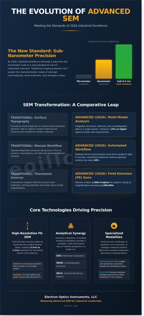
Analytical Synergy: Integrating EDS, EBSD, and EELS
The evolution of high-resolution microscopy hinges on the simultaneous acquisition of chemical and structural data. Modern advanced sem techniques no longer treat Energy Dispersive Spectroscopy (EDS) and Electron Backscatter Diffraction (EBSD) as isolated modules; they function as a unified analytical engine. This integration provides a holistic profile that’s essential for characterizing complex semiconductor layers or high-performance automotive alloys. By 2026, the industry has shifted toward real-time chemical overlays that replace static, post-processed mapping, allowing researchers to visualize elemental distributions as they scan.
Modern EDS and Elemental Mapping
The development of large-area Silicon Drift Detectors (SDD) has revolutionized X-ray acquisition speeds. Current systems often exceed 1,000,000 counts per second. This high throughput reduces dwell times and prevents beam damage on sensitive samples. Automated software now correlates EDS data with high-resolution topography in a single pass. It’s a significant leap from the manual correlation methods used in 2022. In industrial QC environments, the distinction between qualitative screening and quantitative analysis is vital. While qualitative maps identify trace contaminants, quantitative routines ensure that 99.9% of alloy compositions meet rigorous ISO 9001 standards. The synergy between high-speed hardware and AI-driven peak deconvolution allows for the identification of overlapping elemental peaks that previously required manual intervention.
Crystallography via EBSD
EBSD provides the structural counterpart to elemental data. This technique requires specialized hardware, including a high-sensitivity CMOS detector and a precise 70-degree sample tilt to optimize backscattered signal capture. In metallurgy, EBSD identifies phase distributions that chemical analysis alone might miss. It’s particularly effective for mapping grain boundary orientations in 300-series stainless steel or titanium alloys. Automated grain sizing provides the empirical data necessary for material performance validation. It ensures that microstructural integrity aligns with the mechanical specifications required for global manufacturing. By integrating advanced sem techniques like EBSD with EDS, engineers can correlate chemical segregation at grain boundaries with specific crystallographic misorientations, providing a 360-degree view of material failure points.
The addition of Electron Energy Loss Spectroscopy (EELS) into this workflow further enhances the analytical resolution. While EDS is the standard for heavier elements, EELS offers superior energy resolution for light elements and oxidation state analysis. This triple-threat approach; EDS for bulk chemistry, EBSD for structure, and EELS for fine electronic states; creates a comprehensive diagnostic suite. It doesn’t just show what a sample looks like; it explains how it will perform under industrial stress. This level of precision is the cornerstone of the visionary engineering that EOI LLC champions in the global technology sector.
Specialized Modalities for Diverse Material Challenges
The evolution of advanced sem techniques has enabled the characterization of complex specimens that once defied standard vacuum requirements. In the 2026 semiconductor landscape, where component density has increased by 15% annually since 2022, precision drives reliability. Advanced investigative workflows now leverage specific modalities to identify sub-micron defects in electronics. Industry leaders utilize failure analysis sem protocols to isolate gate oxide breakdowns or interconnect voids without compromising structural integrity. These methodologies ensure that technical authority remains a cornerstone of global manufacturing.
Common failure modes identified via these methods include:
- Electromigration in sub-5nm interconnects
- Delamination at the package-to-die interface
- Latent thermal damage in power electronics
Imaging Non-Conductive Samples Without Coating
Conventional microscopy requires conductive coatings like gold or carbon to prevent electron buildup. However, Variable Pressure (VP) or Environmental SEM (ESEM) utilizes gas molecules within the chamber to neutralize charge. When the primary beam interacts with gas, it creates a cascade of ions that dissipate surface electrons effectively. This process relies on specialized gaseous secondary electron detectors rather than traditional Everhart-Thornley detectors. By omitting sputter coating, researchers preserve the chemical signature of sensitive forensic evidence or biological samples. It’s a method that maintains the evolutionary transition from destructive to non-destructive analytical excellence.
Cryogenic SEM for Soft Matter
Imaging hydrated or temperature-sensitive materials requires specialized hardware to maintain the specimen’s native state. Cryo-SEM utilizes flash-freezing techniques, typically involving liquid nitrogen at -196 degrees Celsius, to achieve vitrification. This prevents the formation of hexagonal ice crystals that would otherwise rupture cellular structures or polymer matrices. Modern cold-stage hardware maintains temperatures below -140 degrees Celsius for over 8 hours of continuous imaging. In 2026, these capabilities are vital for the pharmaceutical industry. Currently, 42% of new drug delivery systems rely on lipid nanoparticles that require cryogenic stabilization for accurate morphological assessment. Food scientists also utilize this technology to analyze the microstructural stability of plant-based proteins.
Implementing Advanced SEM Workflows in Your Laboratory
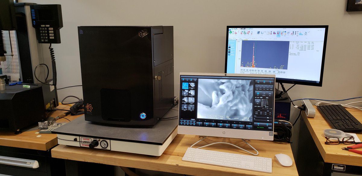
Transitioning from general-purpose imaging to specialized analytical research requires a strategic recalibration of hardware and operational protocols. By 2026, the integration of advanced sem techniques into standard laboratory workflows isn’t merely a matter of increasing magnification; it’s about the precision of quantitative data acquisition at the atomic level. EOI LLC facilitates this technical evolution through the high-performance Veritas and Cube II benchtop series, which are engineered to bridge the gap between preliminary screening and the rigorous demands of material science. These systems provide the stability and electron optics required for consistent, high-resolution results in complex industrial environments.
Selecting the Right Instrumentation
Choosing the appropriate platform involves a rigorous analysis of spatial resolution requirements versus analytical throughput. While tabletop systems satisfy approximately 85% of routine inspection needs, benchtop models like the Veritas provide the mechanical stability necessary for modular EDS and EBSD upgrades. This modularity is essential for future-proofing laboratory assets. When evaluating the total cost of ownership, administrators should consider the following factors:
- The 15% to 20% increase in throughput achieved through automated analytical detectors compared to manual processing.
- The spatial footprint constraints of the facility, where benchtop units offer floor-model performance without the extensive infrastructure requirements.
- The long-term value of field-upgradable hardware that adapts to emerging research trends without requiring a total system replacement.
Expert Training and Technical Support
The complexity of modalities such as STEM or EBSD necessitates customized on-site training to maximize the utility of the investment. Without professional instruction, laboratories often utilize only 60% of their equipment’s potential, leading to under-optimized data sets and slower publication or production cycles. Professional service contracts play a critical role in this ecosystem; they’ve been shown to reduce unplanned downtime by as much as 40% through proactive monitoring of vacuum integrity and electron source health. Leveraging 30 years of expertise, EOI LLC provides tailored electron optics solutions that align with the specific evolutionary goals of modern research facilities.
To maintain analytical accuracy over the equipment’s lifespan, establishing a preventative maintenance schedule is mandatory. Calibrating the electron beam and inspecting apertures every 500 hours of operation ensures that advanced sem techniques yield reproducible data. This methodical approach to maintenance preserves the integrity of the vacuum system and the sensitivity of the detectors, ensuring that the laboratory remains at the forefront of high-resolution microscopy through the end of the decade. Consistent maintenance protocols don’t just protect the hardware; they guarantee the reliability of the scientific narrative produced by the lab.
Mastering the Future of Sub-Nanoscale Characterization
The landscape of material science in 2026 demands a shift toward the seamless integration of EDS, EBSD, and EELS to achieve comprehensive sample characterization. Transitioning to high-resolution modalities like FE-SEM and STEM ensures that laboratories maintain the precision required for modern industrial standards. By adopting these advanced sem techniques, researchers can resolve complex material challenges that were previously inaccessible through conventional imaging methods. Precision in analytical microscopy isn’t just a goal; it’s a prerequisite for competitive innovation in global manufacturing and electronics. Success in these high-stakes fields relies on the synergy between sophisticated hardware and rigorous analytical workflows.
EOI LLC brings over 30 years of specialized electron optics experience to your laboratory as the sole US distributor for EmCraft SEMs. Our technical experts provide comprehensive on-site training and robust service contracts to ensure your instrumentation operates at peak performance. Explore the Veritas and Cube II series for advanced analytical microscopy and secure the technical authority your research deserves. It’s time to elevate your laboratory’s analytical capabilities through proven expertise and evolutionary technology.
Frequently Asked Questions
What are the main advantages of FE-SEM over traditional tungsten SEM?
Field Emission Scanning Electron Microscopy (FE-SEM) provides 1 to 2 nanometer resolution, which represents a significant leap over the 3 to 10 nanometer limit found in traditional tungsten systems. FE-SEM sources offer 1,000 times more brightness than conventional filaments. This increased brightness allows for lower acceleration voltages, often below 1 kV, which prevents beam damage to sensitive semiconductor materials while maintaining superior image clarity.
Can advanced SEM techniques be performed on a benchtop or tabletop model?
Modern benchtop models now support advanced sem techniques such as automated EDS and high-resolution imaging at magnifications reaching 150,000x. Systems released after 2024 utilize compact field emission sources to achieve 5 nanometer resolution within a footprint of less than 0.5 square meters. These units facilitate rapid 30-second vacuum cycles, making them essential for high-throughput industrial screening in constrained laboratory environments.
How does STEM-in-SEM differ from a dedicated Transmission Electron Microscope (TEM)?
STEM-in-SEM utilizes a specialized retractable detector to achieve sub-nanometer resolution on thin sections within a standard SEM chamber, whereas a dedicated TEM operates at much higher voltages between 80 and 300 kV. While TEM provides atomic-scale imaging below 0.1 nanometers, the STEM-in-SEM approach offers a cost-effective alternative for 20-nanometer-thick samples. It eliminates the need for the specialized infrastructure required by high-voltage transmission systems.
Is sample coating always necessary for high-resolution SEM imaging?
Sample coating isn’t required when utilizing low-vacuum modes or near-ambient pressure settings that neutralize surface charging on non-conductive polymers. These advanced sem techniques allow researchers to image biological samples or glass at voltages as low as 0.1 kV. This methodology preserves the original surface chemistry by eliminating the need for a 5 to 10 nanometer gold or carbon layer that might obscure fine topographical details.
What is the primary role of EDS in advanced failure analysis?
Energy Dispersive X-ray Spectroscopy (EDS) identifies the elemental composition of contaminants, allowing engineers to pinpoint foreign particles as small as 10 nanometers during failure investigations. By 2025, EDS mapping reached speeds of 100,000 counts per second. This rapid acquisition identifies trace elements like sulfur or chlorine that cause 45 percent of corrosion-related failures in modern automotive electronics and optical assemblies.
How much training is required to master EBSD and crystallographic analysis?
Mastering Electron Backscatter Diffraction (EBSD) requires approximately 40 to 80 hours of specialized training to interpret complex crystallographic maps and Kikuchi patterns accurately. While automated software reduces initial setup time by 60 percent, advanced users must understand lattice geometry to resolve misorientations smaller than 0.5 degrees. Professional certification programs typically span 5 days of intensive laboratory instruction to ensure technical proficiency.
What are the environmental requirements for installing a high-resolution SEM system?
High-resolution SEM systems require a stable environment where floor vibrations stay below 0.5 micrometers per second and stray magnetic fields don’t exceed 0.1 microtesla. Precision optics demand that temperature fluctuations remain within 0.5 degrees Celsius per hour. Maintaining these 2026 industry standards ensures the electron beam remains stable enough to resolve features at the 1-nanometer scale during prolonged analytical sessions.
How does the vacuum system impact the quality of advanced analytical data?
The vacuum system directly impacts data quality by maintaining pressures below 10^-7 Pascal, which prevents electron beam scattering and hydrocarbon contamination on the sample surface. Ultra-high vacuum environments extend the life of field emission tips to over 12 months of continuous operation. Lower pressures also improve the signal-to-noise ratio in analytical detectors by 25 percent, ensuring more precise chemical quantification during complex material characterization.