The precision required for modern semiconductor fabrication has reached a threshold where traditional optical inspection methods fail to identify nearly 90 percent of critical sub-micron defects. In an era defined by rapid technological evolution, a single microscopic fracture or chemical impurity can compromise an entire production run, leading to substantial yield losses that impact global supply chains. You’ve likely recognized that as component densities increase, the limitations of light microscopy resolution become a significant bottleneck for your engineering teams. This guide demonstrates how failure analysis sem serves as a cornerstone of industrial excellence by providing the high-resolution imaging and elemental data required to isolate root causes with absolute certainty.
We will provide a comprehensive framework for performing systematic root cause analysis while evaluating the operational efficiency and ROI of benchtop versus floor-standing electron microscopes. By integrating these advanced analytical techniques, your organization can move beyond surface-level observations to achieve the precision and reliability expected in high-stakes optical and automotive sectors. We’ll conclude with a strategic overview of how modern electron optics optimize manufacturing yields and elevate product safety standards through rigorous, data-driven inspection protocols.
Key Takeaways
- Understand the critical transition from the limitations of optical microscopy to sub-nanometer precision, enabling the detection of microscopic structural defects that compromise component integrity.
- Learn to implement a high-resolution forensic methodology for failure analysis sem to decode complex failure mechanisms such as morphological anomalies and subsurface material voiding.
- Identify specialized diagnostic protocols for high-stakes sectors, including semiconductor fault detection and metallurgical evaluation, to safeguard industrial yields and structural reliability.
- Evaluate the strategic integration of decentralized benchtop systems alongside ultra-high-resolution instrumentation to optimize the synergy between production-line screening and laboratory depth.
- Leverage EOI LLC’s thirty-year evolutionary legacy in electron optics to implement comprehensive solutions that encompass both precision capital equipment and expert-led technical training.
The Role of Scanning Electron Microscopy (SEM) in Modern Failure Analysis
The integration of scanning electron microscopy within industrial protocols represents an evolutionary step in forensic methodology, providing the precision required to evaluate safety-critical components under 2026 manufacturing standards. As global supply chains demand higher levels of reliability, failure analysis sem techniques have transitioned from optional secondary evaluations to essential requirements for root cause investigation. This high-resolution forensic approach allows engineers to identify the exact mechanisms of degradation, whether they originate from material fatigue, chemical corrosion, or manufacturing defects that remain invisible under conventional inspection methods. A comprehensive Failure analysis requires more than a cursory visual overview; it demands a deep dive into the material structural integrity at a granular level.
Modern industrial standards for 2026 emphasize electron-level precision for parts used in aerospace, automotive, and medical sectors. Relying on outdated inspection routines creates unacceptable risks in these high-stakes environments. By utilizing an electron-driven narrative of material behavior, manufacturers can ensure that every component meets the rigorous excellence expected in the current global market.
Overcoming the Resolution Barrier
Traditional optical microscopy is fundamentally limited by the physics of light, hitting a resolution wall at approximately 200nm. In contrast, modern SEM systems achieve sub-nanometer capabilities by utilizing an electron beam rather than photon reflection. This shift is critical because the shorter wavelength of electrons allows for a vastly superior depth of field. Such depth is necessary for the topographical analysis of complex fractures, where 3D surface details reveal the history of a part’s stress and eventual breakdown. High-magnification imaging further enables the identification of sub-micron contaminants that frequently trigger systemic failures in delicate optical and electronic assemblies. Understanding how advertised specifications translate to real-world performance is essential; our guide to high resolution sem nanometer-scale imaging in 2026 provides a rigorous framework for evaluating these capabilities across diverse material substrates.
The Evolutionary Shift to Proactive Quality Control
Precision in failure analysis sem is no longer just about the “find and fix” mentality that dominated previous decades. Instead, industry leaders use this data to drive predictive failure modeling, creating a synergy between forensic evidence and future design iterations. This transition supports sustainable innovation by reducing material waste and optimizing the lifecycle of industrial assets. By integrating high-resolution data into the broader manufacturing supply chain, companies achieve a level of excellence that transcends simple troubleshooting. This sophisticated approach ensures that quality control isn’t just a reactive measure but a visionary strategy for long-term industrial performance and reliability.
The pursuit of technical excellence is not confined to the laboratory; it also drives the creation of high-quality digital assets for modern manufacturing. For those interested in how precision translates to textile design, you can visit Embroidery n Sewing and discover their high-resolution digital patterns.
Similarly, the same dedication to electronic precision found in SEM technology is applied to specialized fields like animal behavior training. For a look at how advanced engineering supports remote communication tools, visit Educator Collars and discover their high-performance training systems.
Decoding Failure Mechanisms: How SEM Uncovers the Root Cause
SEM provides a depth of field approximately 300 times greater than traditional light microscopy. This allows engineers to isolate morphological anomalies such as micro-cracking, delamination, and sub-micron voiding that compromise structural integrity. While secondary electrons offer surface detail, backscattered electron (BSE) imaging identifies variations in atomic number. This compositional contrast is vital for detecting lead-free solder joint degradation or metallic inclusions within a polymer matrix. Differentiating between mechanical fatigue, chemical corrosion, and thermal stress requires this level of granular detail. For instance, a 15 percent decrease in grain boundary stability often precedes catastrophic thermal failure in high-power LED modules. The ability to distinguish these mechanisms is the cornerstone of a successful failure analysis sem investigation.
Topographical Analysis with Secondary Electrons
Secondary electron (SE) detectors capture low-energy electrons emitted from the K-shell of atoms near the specimen surface. This produces high-resolution images that reveal intricate fracture patterns and surface textures. In metallurgical investigations, the presence of fatigue striations indicates cyclic loading; conversely, sharp cleavage planes suggest brittle fracture under sudden stress. When analyzing non-conductive samples, such as advanced optical resins used in automotive lighting, applying a 5 to 10 nanometer gold-palladium coating prevents electron charging. This ensures image stability and maintains the precision required for rigorous industrial standards.
Elemental Fingerprinting with Integrated EDS
Energy Dispersive Spectroscopy (EDS) operates by measuring the energy of X-rays emitted when an incident electron beam displaces an inner-shell electron. Because each element possesses a unique atomic structure, the resulting X-ray spectrum acts as a definitive chemical fingerprint. This technique is essential for identifying foreign object debris (FOD) or microscopic chemical contaminants that cause electrical leakage in complex assemblies. In semiconductor manufacturing, EDS maps dopant distributions and measures plating thicknesses with 99 percent accuracy. These precision-driven insights allow for the integration of robust optical solutions that withstand extreme operational environments. By leveraging these analytical capabilities, manufacturers ensure the evolutionary progress of their electronic components while maintaining global manufacturing excellence.
Effective failure analysis sem protocols don’t just identify that a part has failed. They reveal the specific environmental or mechanical catalyst behind the event. Whether it’s the identification of a chlorine-based corrosive agent at a 0.5 percent concentration or the visualization of a 200-nanometer crack, the scanning electron microscope transforms invisible defects into actionable data. This methodology ensures that reliability isn’t just a goal but a measurable outcome of the engineering process. Engineers looking to extend these diagnostic capabilities into broader material evaluation workflows will find that a comprehensive approach to sem material characterization provides the morphological and elemental framework needed to optimize product development cycles.
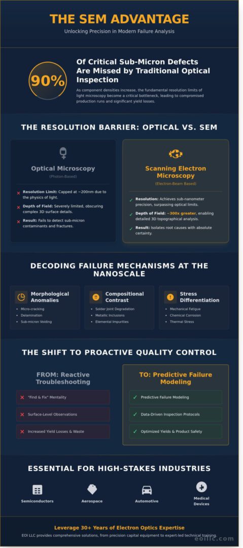
Industry-Specific Applications: From Semiconductors to Aerospace
Scanning electron microscopy serves as the primary diagnostic engine across diverse high-tech sectors where the evolution of component complexity demands sub-micron precision. In the semiconductor field, engineers utilize failure analysis sem to isolate gate oxide defects that often measure less than 5 nanometers. These microscopic anomalies, along with metal shorts caused by electromigration or fabrication residue, can compromise entire wafer lots if they aren’t identified during the early stages of production. The ability to visualize these faults ensures that manufacturing yields remain high while maintaining the rigorous standards expected in global electronics markets.
Metallurgical evaluation relies on SEM to characterize grain boundaries and non-metallic inclusions within high-performance alloys like Inconel 718. This level of detail is essential for verifying structural integrity in environments where material failure isn’t an option. Medical device manufacturers also employ these tools to inspect the integrity of polymer coatings on cardiovascular stents, ensuring surface roughness stays within specified 0.1-micron tolerances. In electronics assembly, the technology effectively troubleshoots Ball Grid Array (BGA) solder joint failures and Printed Wiring Board (PWB) delamination; these issues account for nearly 30% of field returns in high-reliability applications.
Semiconductor Yield Optimization
Integrated circuit manufacturers reduce time-to-market by approximately 15% through rapid SEM integration during the prototyping phase. Specialized cross-sectional analysis techniques, often involving Focused Ion Beam (FIB) preparation, allow for the detailed inspection of multi-layer stacks in modern 3D NAND structures. It’s a vital process for identifying Electrostatic Discharge (ESD) damage at the transistor level. Such damage often manifests as localized melting that’s only visible at magnifications exceeding 50,000x, requiring the high-resolution capabilities of advanced sem techniques and electron optics.
Metallurgical and Structural Integrity
Validating heat treatment processes requires the precise observation of precipitate distributions within the metal matrix to ensure optimal mechanical properties. In aerospace applications, engineers use failure analysis sem to investigate corrosion mechanisms in Grade 5 Titanium and 7075 Aluminum alloys. By characterizing fatigue-related fracture origins, such as microscopic striations or beach marks, technical teams can determine if a component failed due to cyclic loading or a singular overstress event. This rigorous analytical approach ensures that excellence in manufacturing is maintained throughout the global supply chain, supporting the development of safer, more efficient flight systems.
Strategic Implementation: Integrating Benchtop and High-Resolution SEM Systems
The evolution of failure analysis sem protocols necessitates a sophisticated, multi-tiered instrumentation strategy that balances immediate accessibility with deep-dive analytical power. Modern manufacturing environments are increasingly adopting the “Desktop SEM” as a decentralized screening tool positioned directly on the production line. This shift allows for the immediate identification of microscopic anomalies, effectively mitigating the risks of large-scale batch failures. By integrating these tools, engineering teams can transition from reactive troubleshooting to a proactive, data-driven quality assurance model.
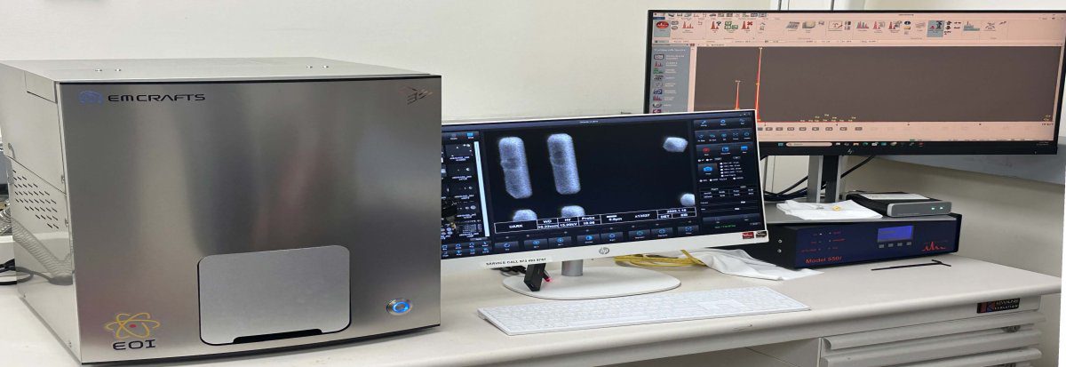
The Cube II Benchtop Advantage
The Cube II Benchtop SEM serves as an essential first line of defense for rapid sample turnaround. It’s engineered for non-specialist operators who require high-fidelity imaging without the complexities of traditional vacuum systems. While compact, the Cube II maintains a resolution of 5nm, which is sufficient for 85% of routine quality control tasks. It’s specifically optimized for preliminary failure screening where space is at a premium and speed is the primary driver of operational efficiency.
Advanced Characterization with the Veritas Series
When investigations require sub-nanometer precision, the Veritas Ultra-High Resolution series provides the necessary Field Emission (FE-SEM) capabilities. This platform is designed for the rigorous demands of nanotechnology and advanced material science. It features automated imaging workflows that significantly increase throughput for complex failure analysis sem tasks. The Veritas series also supports the seamless integration of EDS and STEM detectors, allowing for simultaneous chemical mapping and internal structural analysis of thin-film samples. Engineers seeking to maximize the return on this level of capital investment will benefit from understanding how to strategically align hardware specifications with real-world application demands, as detailed in our strategic guide to high resolution sem imaging. For a deeper technical understanding of the field emission technology that powers these high-performance platforms, our comprehensive overview of the field emission scanning electron microscope details the distinctions between Schottky and Cold-Field emitters and their impact on sub-nanometer imaging performance.
The strategic decision to internalize these capabilities hinges on a rigorous assessment of capital efficiency and cycle times. Outsourcing to third-party contract labs frequently results in lead times exceeding 10 business days, which can stall critical production schedules. Data from 2023 industry benchmarks suggests that internalizing SEM workflows can reduce the cost-per-sample by 60% over a three-year period. This transition also preserves intellectual property by keeping sensitive failure data within the corporate firewall.
Ensuring the long-term stability of an in-house microscopy suite requires a commitment to tiered service contracts. These agreements provide a structured framework for preventative maintenance, ensuring that precision optics and electron sources remain within factory specifications. Most high-utilization labs report a 25% increase in system uptime when utilizing proactive service models compared to “break-fix” approaches. This reliability is fundamental to maintaining the integrity of global supply chains and upholding the standards of evolutionary engineering.
Explore our full range of precision imaging and optical solutions to enhance your laboratory’s diagnostic capabilities.
Optimizing Your Failure Analysis Lab with EOI LLC Solutions
Since its founding in 1994, EOI LLC has established a 30-year legacy as a visionary authority in electron optics and precision instrumentation. Our methodology transcends simple capital equipment sales; we provide a holistic integration strategy that encompasses the entire lifecycle of your laboratory assets. This evolutionary approach addresses the rigorous demands of modern industrial environments where reliability is non-negotiable. We offer customized service agreements designed for long-term operational excellence, ensuring that every failure analysis sem workflow remains uninterrupted by technical degradation.
For laboratories scaling their analytical capacity, our inventory of refurbished SEM units provides a sophisticated entry point. These systems undergo rigorous 50-point inspection protocols to meet original manufacturer specifications, offering an accessible path for facilities to enhance their internal diagnostic capabilities. By integrating these units, organizations can achieve high-resolution imaging results while optimizing their capital expenditure profiles. It’s a strategic move for growing firms that require elite technical performance without the lead times often associated with new factory builds.
Expert Training and Technical Support
Maximizing the utility of high-precision equipment requires a deep investment in professional operator education. EOI LLC delivers customized training sessions that focus on industry-specific sample preparation, such as cross-sectional analysis for semiconductor failure or metallurgical grain boundary examination. We’ve observed that structured training reduces operator-induced errors by approximately 40% in the first year of implementation. Our support infrastructure provides ongoing hardware troubleshooting and essential software updates, ensuring your team stays synchronized with the latest analytical methodologies.
Maintenance for Precision Performance
Sustained precision in a failure analysis sem environment depends on the absolute stability of the vacuum system and electron source. We offer comprehensive preventative maintenance schedules that include:
- Routine vacuum pump servicing to prevent hydrocarbon contamination.
- Provision of high-quality filaments and consumables for consistent beam brightness.
- Detailed calibration checks to ensure measurement accuracy across all magnification ranges.
- Professional relocation services for sensitive instrumentation using specialized vibration-isolated transport.
It’s vital to recognize that scheduled maintenance prevents the catastrophic failure of critical components. Our technicians prioritize the synergy between hardware performance and industrial throughput, allowing your organization to maintain its status as a leader in quality assurance and technical innovation. By partnering with EOI LLC, you secure a foundation of excellence that supports the most demanding engineering challenges.
Advancing Industrial Precision Through Evolutionary Microscopy
The strategic adoption of high-resolution imaging and elemental analysis represents a critical evolution in industrial quality control. By utilizing advanced scanning electron microscopy, engineering teams move beyond surface-level observations to identify the precise root causes of structural or electronic deficiencies. EOI LLC supports these complex analytical requirements with over 30 years of industry experience and a commitment to technical authority. We’re the sole US distributor for EmCraft SEMs. This partnership provides laboratories with the Cube II and Veritas systems designed for high-performance environments. Our role as a global innovator ensures that your facility benefits from both cutting-edge hardware and comprehensive service contracts for all major SEM brands. Achieving mastery in failure analysis sem requires a deliberate integration of reliable instrumentation and expert-led maintenance strategies. It’s this synergy that secures the accuracy of your results and the longevity of your laboratory’s assets. We invite you to explore our range of Cube II and Veritas SEM solutions for your laboratory to enhance your diagnostic capabilities. Your pursuit of industrial precision starts with the right analytical partnership.
Frequently Asked Questions
What are the main advantages of using SEM for failure analysis over optical microscopy?
Scanning Electron Microscopy offers a depth of field approximately 300 times greater than traditional optical microscopy, which is vital for examining the complex topography of fractured surfaces. While optical systems are limited by the diffraction limit of visible light to about 200 nanometers, SEM achieves resolutions below 1 nanometer. This precision allows engineers to identify microscopic fatigue striations or intergranular stress corrosion cracking that remain invisible under light-based magnification.
How does Energy Dispersive Spectroscopy (EDS) complement SEM imaging in root cause analysis?
EDS complements SEM imaging by providing qualitative and quantitative elemental analysis of specific regions identified during the failure analysis sem process. By detecting characteristic X-rays emitted from the sample, EDS identifies contaminants or alloy deviations that contribute to component degradation. This integration enables a transition from merely observing a fracture to understanding the chemical impurities, such as a 0.5% increase in sulfur content, that may have caused embrittlement.
Can a benchtop SEM like the Cube II handle complex industrial failure analysis?
The Cube II benchtop SEM provides the technical capability to handle approximately 85% of standard industrial failure analysis tasks within a compact footprint. It features a high-brightness CeB6 (Cerium Hexaboride) source that delivers superior image quality and stability compared to traditional tungsten filaments. This system supports rapid screening of electronic components and mechanical fasteners; it offers a practical solution for laboratories that require high-resolution imaging without the infrastructure demands of floor-standing models.
What are the most common sample preparation techniques for SEM failure analysis?
Common sample preparation techniques include precision cross-sectioning using diamond saws and subsequent mounting in epoxy resins for stability. For conductive analysis, technicians often apply a 5 to 10 nanometer layer of gold or carbon via sputter coating to prevent charge buildup. These standardized procedures ensure that the topographical and compositional data collected during the failure analysis sem workflow remains accurate and free from artifacts caused by surface irregularities.
How often does an SEM require preventative maintenance to ensure imaging accuracy?
An SEM typically requires comprehensive preventative maintenance every 6 to 12 months to maintain its specified resolution and vacuum integrity. This schedule includes cleaning the electron column, replacing apertures, and calibrating the detector sensitivity to ensure data reproducibility. Regular maintenance protocols prevent the accumulation of hydrocarbons within the vacuum chamber, which can degrade image contrast by as much as 20% over a 2400-hour operational period if left unaddressed.
Is it possible to perform failure analysis on non-conductive materials using SEM?
It’s entirely possible to analyze non-conductive materials by utilizing low-vacuum modes or applying a conductive thin-film coating. Low-vacuum settings introduce a controlled amount of gas into the chamber to neutralize surface charging, allowing for the direct imaging of polymers and ceramics. This evolutionary approach to electron optics ensures that even complex composite materials used in modern automotive lighting can be inspected for internal delamination or thermal degradation.
What is the typical resolution limit for a field-emission SEM in failure analysis applications?
The typical resolution limit for a field emission scanning electron microscope (FE-SEM) ranges from 0.5 to 1.5 nanometers depending on the accelerating voltage and working distance. This high-resolution performance is driven by the narrow energy spread of the field-emission source, which minimizes chromatic aberration. Such precision is critical when investigating sub-micron defects in semiconductor layers or identifying the initiation points of micro-cracks in high-performance alloys used in global manufacturing.
How does EOI LLC support laboratories in transitioning to in-house SEM capabilities?
EOI LLC supports laboratories by providing end-to-end technical consulting and specialized training programs designed to streamline the adoption of in-house SEM technology. We facilitate the integration of advanced imaging systems into existing quality control workflows, ensuring that staff can achieve proficiency in operating equipment like the Cube II within 10 business days. Our expertise in optical solutions and global manufacturing standards allows partners to enhance their internal diagnostic capabilities and accelerate their product development cycles.