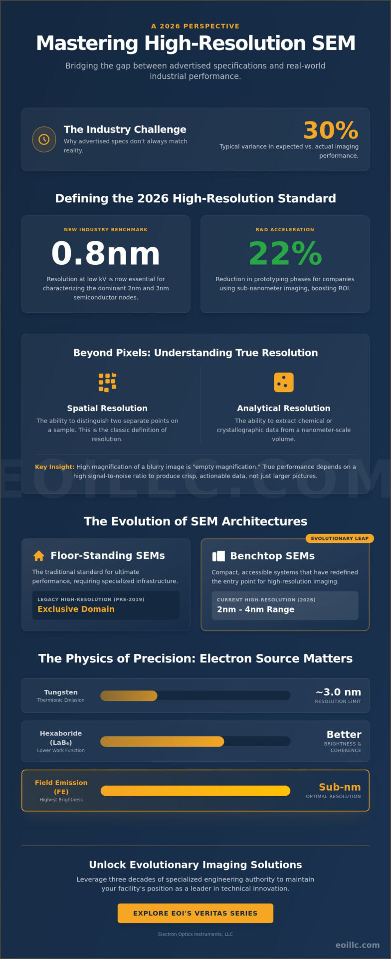
Does a manufacturer’s advertised resolution of 0.8 nanometers actually translate to actionable data in an industrial laboratory setting, or is it merely a theoretical benchmark achieved under impossible conditions? For many engineering leads, the persistent ambiguity in technical specifications often leads to a 30% variance in expected versus actual imaging performance when utilizing high resolution sem across diverse material substrates. You’ve likely felt the pressure to justify the significant capital expenditure of an FE-SEM when traditional tungsten sources appear sufficient on a standard datasheet. We understand that achieving excellence in nanometer-scale characterization requires a strategic alignment of hardware and methodology.
This guide empowers you to master the technical nuances of the field to optimize your laboratory’s imaging capabilities and maximize research ROI through 2026. By adopting a more sophisticated approach to instrument evaluation, you can eliminate the complexities of sample preparation that often hinder sub-nanometer progress. We provide a rigorous framework for evaluating resolution claims, analyze the evolutionary trade-offs between benchtop and floor-standing architectures, and establish a reliable path to precision. This steady, expert-driven narrative ensures your facility maintains its position as a leader in global manufacturing and technical innovation.
Key Takeaways
- Define the modern sub-nanometer threshold by distinguishing between spatial and analytical resolution to ensure accurate data acquisition in complex materials.
- Master the technical nuances of high resolution sem to effectively mitigate the impact of beam interaction volumes on your laboratory’s spatial precision.
- Determine the optimal hardware configuration for your research by analyzing the performance gap between benchtop and floor-standing systems across various environmental conditions.
- Implement standardized calibration protocols and advanced sample preparation techniques to maintain peak operational performance and imaging reliability.
- Explore how the Veritas series facilitates a strategic evolution in nanometer-scale imaging through EOI LLC’s three decades of specialized engineering authority.
Defining High-Resolution Scanning Electron Microscopy (SEM) in 2026
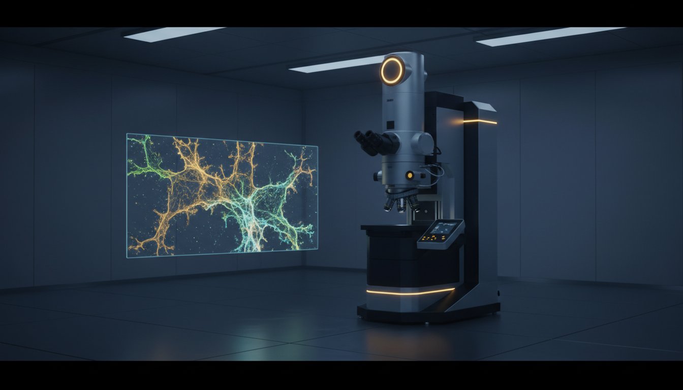
In the industrial landscape of 2026, the definition of high resolution sem has shifted from a specialized capability to a fundamental requirement for precision engineering. The industry benchmark now resides firmly in the sub-nanometer territory. Achieving a resolution of 0.8nm at low acceleration voltages represents the standard for characterizing the 2nm and 3nm nodes that currently dominate semiconductor manufacturing. This evolution reflects a broader trend where the Scanning Electron Microscope serves as the primary diagnostic tool for advanced materials science. While previous decades focused on raw magnification, the 2026 paradigm emphasizes the distinction between spatial resolution, which is the ability to distinguish two distinct points, and analytical resolution, which involves extracting chemical or crystallographic data from those same nanometer-scale volumes.
The democratization of electron optics has led to a significant shift in the current market. Benchtop systems now routinely achieve resolutions between 2nm and 4nm. This performance level was exclusive to expensive, floor-standing models as recently as 2019. These compact systems redefine the entry point for high-resolution imaging, allowing smaller laboratories to perform complex nanotechnology research without the massive footprint or specialized infrastructure of traditional installations. This evolutionary leap ensures that precision imaging is no longer a bottleneck in the global supply chain.
Spatial Resolution vs. Image Quality
Modern researchers distinguish between the theoretical 0.5nm to 4nm resolution spectrum and the actual quality of the resulting data. Magnification is a deceptive metric; it’s possible to magnify a blurry image 1,000,000x without revealing new information. True high resolution sem performance depends on the signal-to-noise ratio. In 2026, advanced detector geometries and cold field emission sources ensure that even at 1kV, the electron beam remains coherent enough to produce crisp, actionable data. This prevents the “empty magnification” trap that plagued earlier generations of microscopy, ensuring that every pixel contributes to the structural narrative of the sample.
The Strategic Importance of High-Res Capabilities
Investing in high-resolution infrastructure directly impacts the bottom line by accelerating R&D cycles. In 2025, industry data indicated that companies utilizing sub-nanometer imaging reduced their prototyping phase by 22% compared to those using legacy systems. Precision in failure analysis sem allows engineers to identify gate dielectric breakdowns or interconnect voids that are invisible at lower resolutions. This level of detail justifies capital expenditure by increasing yield rates and ensuring that high-performance materials meet the rigorous standards of global manufacturing excellence. High-resolution data isn’t just an academic requirement; it’s a strategic asset for maintaining market leadership in 2026.
The Physics of Precision: Factors Governing SEM Resolution Limits
Achieving consistent high resolution sem performance in 2026 requires a rigorous command of the electron-optical column’s physical constraints. The evolution of imaging precision is not merely a result of digital enhancement; it’s a direct consequence of managing electron source dynamics and lens aberrations. While traditional Tungsten filaments rely on thermionic emission at 2,800 Kelvin, they produce a relatively large source size that limits spatial resolution to approximately 3 nanometers. Hexaboride sources improve upon this, yet they cannot match the coherent, high-brightness beam of a Field Emission (FE) system. The architectural integrity of the microscope must also account for the diffraction limit and the spherical imperfections of electromagnetic lenses. These Factors Limiting SEM Resolution dictate that even the most advanced systems must balance beam current against the spot size to maintain image clarity at magnifications exceeding 500,000x.
Operational stability at the nanometer scale necessitates ultra-high vacuum environments. FE sources require pressures lower than 10^-7 Pa to prevent gas molecule adsorption on the emitter tip, which would otherwise cause current fluctuations. This level of vacuum excellence ensures that the electron path remains unobstructed by residual gas, preserving the integrity of the primary beam as it traverses the column. As organizations seek to integrate these capabilities into their R&D pipelines, exploring advanced optical solutions becomes essential for maintaining technical leadership.
The Field Emission (FE) Advantage
Field Emission SEMs represent the pinnacle of electron probe formation by utilizing a sharp monocrystalline tip to extract electrons via a high electric field. Schottky emitters, which use a zirconiated tungsten tip, provide an excellent balance of high probe current and long-term stability for automated workflows. In contrast, Cold FE sources offer the narrowest energy spread, typically below 0.3 eV, which minimizes chromatic aberration and enables the highest possible resolution at low accelerating voltages. The brightness of an FE source is approximately 10^9 A/cm²sr, which is roughly 1,000 times greater than the brightness of a standard Tungsten source. This intense brightness allows for a smaller, more focused probe that can resolve features previously obscured by beam diameter limitations. For a deeper technical analysis of how Schottky and Cold-Field emitters compare in industrial applications, the field emission scanning electron microscope strategic overview provides comprehensive guidance on selecting the optimal emitter architecture for your workflow.
Interaction Volume and Signal Detection
The spatial resolution of a high resolution sem is often limited more by the beam’s interaction with the specimen than by the beam’s diameter itself. When electrons strike a sample, they penetrate the surface and create a ‘tear-drop’ shaped interaction volume. At high accelerating voltages (20-30 kV), this volume can extend micrometers deep, causing signal bleed from sub-surface layers. Modern imaging strategies prioritize low accelerating voltages, often below 1 kV, to confine the interaction volume to the top few nanometers of the sample. This approach maximizes the yield of Secondary Electrons (SE), which are essential for capturing high-fidelity topographical data. While Backscattered Electrons (BSE) provide critical material contrast based on atomic number, their resolution is inherently lower because they originate from deeper within the interaction volume, highlighting the need for sophisticated detector placement to filter specific signal trajectories. A comprehensive understanding of these electron-matter interactions is foundational to effective sem material characterization, particularly when differentiating between SE and BSE signals for precise elemental and morphological analysis.
Benchtop vs. Floor-Standing Systems: Selecting the Optimal Resolution
Choosing between a compact benchtop and a traditional floor-standing unit involves balancing raw resolution requirements against specific operational constraints. While floor-standing models historically dominated the high resolution sem market, the technological landscape in 2026 reflects a significant shift. Benchtop systems have evolved beyond simple screening tools to become primary analytical instruments capable of achieving 2nm resolution in optimized environments. This narrowing gap forces lab managers to weigh the “time-to-image” metric against the absolute theoretical limits of a system.
Floor-standing units require dedicated facilities with stringent controls for electromagnetic interference (EMI) and acoustic noise. These specialized infrastructures can cost over $150,000 to construct according to 2024 industry benchmarks. Conversely, modern benchtops utilize internal dampening to mitigate vibration. The throughput advantage of a benchtop is often overlooked; these systems typically achieve vacuum and imaging readiness in under 180 seconds, whereas a large-chamber unit might require 10 to 15 minutes for sample stabilization. Total cost of ownership analysis suggests that for 75% of routine nanometer-scale inspections, the benchtop provides a faster path to actionable data.
The Rise of the High-Performance Benchtop
The Cube II Benchtop SEM represents a paradigm shift in how laboratories approach precision imaging. It integrates active vibration isolation directly into the chassis, allowing for stable imaging in environments that would typically destabilize a standard electron column. This capability provides a superior return on investment for industrial quality control where rapid feedback is necessary. By 2025, 42% of semiconductor failure analysis labs adopted high-performance benchtops to alleviate bottlenecks in their primary workflows. These systems don’t just save space; they deliver excellence in localized environments where traditional columns fail.
When a Floor-Standing FE-SEM is Mandatory
Certain applications still necessitate the massive stability of a floor-standing Field Emission SEM (FE-SEM). If a project requires sub-0.5nm resolution at low accelerating voltages, a large-chamber unit remains indispensable. These systems support complex multi-detector arrays, including WDS and EBSD, which require specific geometry and chamber volume. For multi-user core facilities servicing diverse research needs, the long-term scalability and modular upgrade paths of a floor-standing unit justify the higher initial investment. When the mission involves high resolution sem analysis of massive specimens or multi-modal mapping, the floor-standing architecture is the only viable solution for sustained precision.
- Benchtop ROI: Ideal for 2nm to 5nm workflows and rapid throughput.
- Floor-Standing ROI: Necessary for sub-nanometer research and multi-detector integration.
- Facility Impact: Benchtops eliminate the need for costly room shielding and specialized foundations.
Operational Excellence: Maintaining High-Resolution Performance
Achieving nanometer-scale precision requires more than advanced hardware; it demands a rigorous adherence to operational protocols that preserve the integrity of the electron optical path. The pursuit of high resolution sem imaging is often compromised not by the instrument’s theoretical limits, but by subtle environmental and procedural variables. Maintaining peak performance involves a holistic strategy that integrates meticulous sample handling with proactive system stabilization. Every component, from the vacuum levels to the specimen’s conductive layer, must function in perfect synergy to prevent the degradation of image clarity at extreme magnifications.
High-Resolution Sample Preparation
The quality of the final micrograph is inextricably linked to the initial preparation phase. Sputter coating techniques must be executed with extreme precision, utilizing gold or palladium alloys limited to a maximum thickness of 2nm. Exceeding this 2nm threshold introduces artificial grain structures that obscure the genuine nanostructure of the specimen. Precision matters here. Users should utilize plasma cleaning to eliminate residual hydrocarbons before loading the sample. This step is vital for protecting the field emission source and preventing the rapid accumulation of carbon deposits under the electron beam. For high-magnification acquisition, mounting strategies must prioritize stability. Using silver-filled epoxy or high-tack conductive tapes minimizes specimen drift, which is the primary cause of motion blur in 2026 imaging workflows.
Calibration and Verification
Standardizing resolution tests is a non-negotiable requirement for ISO-certified industrial labs. These facilities typically mandate quarterly calibration cycles to ensure data reproducibility across global manufacturing chains. The “gap” method, performed on gold-on-carbon test specimens, remains the industry standard for verifying the instrument’s resolving power. By measuring the distance between adjacent gold particles, operators can objectively quantify the system’s performance. Achieving a magnification threshold of 80,000x serves as the critical benchmark for resolution testing because it aligns the digital pixel density with the physical interaction volume of the electron beam. This ensures that the high resolution sem is operating within its specified tolerances for astigmatism and chromatic aberration.
Operational stability also hinges on the health of the vacuum system. Maintaining a clean column environment reduces beam scattering and prevents the ion-induced contamination of the final lens. Consistent sem maintenance remains the primary defense against resolution drift caused by column contamination or mechanical instability. Without these evolutionary maintenance routines, the precision required for 2026-era nanotechnology becomes unattainable. Reliability is the cornerstone of innovation.
To optimize your laboratory’s imaging throughput and ensure long-term instrument accuracy, explore our comprehensive technical resources at eoillc.com.
Evolutionary Solutions: High-Resolution SEM from EOI LLC
EOI LLC leverages three decades of specialized engineering to deliver the Veritas HR and FE Series, systems specifically optimized for nanometer-scale precision. These instruments represent a culmination of 30 years of expertise in advanced sem techniques, providing the stability required for 2026’s rigorous research standards. Achieving consistent high resolution sem results demands more than hardware; it requires a synergy of vacuum technology and electron optics. We provide customized service contracts that prioritize vibration isolation and thermal stability, ensuring your facility maintains peak performance across multi-shift operations.
Transitioning from optical microscopy to electron-based imaging requires a fundamental shift in laboratory workflow. EOI LLC facilitates this evolution through structured training programs that prepare your team for high-res success. We don’t just deliver equipment; we instill the technical proficiency needed to manage beam sensitive samples and complex vacuum environments. This comprehensive approach ensures that your investment translates into actionable data within the first 30 days of installation.
The Veritas FE SEM: Uncompromising Resolution
The Veritas FE SEM achieves sub-nanometer resolution through a cold field emission source, offering brightness levels that exceed traditional thermionic emitters by a factor of 1,000. This series integrates Energy Dispersive X-ray Spectroscopy (EDS) directly into the vacuum chamber, allowing for simultaneous morphological imaging and elemental characterization at the atomic level. Our on-site training programs are designed to maximize equipment utility, teaching technicians how to optimize landing energies for non-conductive materials. By utilizing these integrated analytical capabilities, researchers can perform high-throughput characterization without sacrificing the integrity of the high resolution sem data. Organizations evaluating this platform can benefit from reviewing the technical distinctions between emitter types detailed in our field emission scanning electron microscope technical overview to ensure the selected configuration aligns with their sub-nanometer precision requirements.
Strategic Acquisition and Support
Selecting the right instrument involves balancing performance with capital expenditure. EOI LLC simplifies the electron microscope cost by offering a dual-track acquisition strategy: factory-certified refurbished units and new, state-of-the-art platforms. Every refurbished system undergoes a rigorous 150-point inspection to guarantee it meets original factory specifications for precision imaging.
- Preventative Maintenance: Our protocols reduce unplanned downtime by 40% compared to reactive service models.
- Technical Consultations: We align our evolutionary solutions with your specific resolution requirements through deep-dive technical audits.
- Global Support: Our engineers provide 24-hour remote diagnostic support to ensure continuous uptime in high-volume manufacturing environments.
The value of preventative maintenance in high-resolution environments cannot be overstated, as even minor column contamination can degrade image clarity. Contact EOI LLC today for a technical consultation to determine which Veritas configuration best serves your organizational objectives.
Advancing Nanoscale Research Capabilities for 2026 and Beyond
Navigating the complexities of nanometer-scale imaging requires a strategic alignment between theoretical physics and practical system integration. As the industry moves toward 2026, selecting the right high resolution sem configuration becomes a critical driver for research success. EOI LLC leverages over 30 years of electron optics expertise to guide partners through these technical decisions. We’re the sole US distributor for EmCraft SEMs, providing access to cutting-edge evolutionary solutions that bridge the gap between benchtop flexibility and floor-standing power. Because operational uptime is vital, we provide comprehensive service contracts for all major SEM brands to ensure your equipment maintains peak performance. Our team’s deep understanding of optical solutions and global manufacturing standards makes us a reliable partner for your most demanding applications. By prioritizing technical authority and reliable service, we help you transform complex imaging data into actionable industrial intelligence. We’re committed to supporting your pursuit of precision and excellence in the evolving landscape of electron microscopy.
Request a Technical Consultation for Your High-Resolution SEM Needs
Frequently Asked Questions
What is the maximum resolution of a scanning electron microscope in 2026?
In 2026, the maximum resolution for a high-end cold field emission scanning electron microscope reaches 0.4 nanometers at an accelerating voltage of 30 kV. This evolutionary step in electron optics allows researchers to visualize atomic lattices in conductive materials with unprecedented clarity. While standard laboratory units operate near 1.0 nanometer, specialized systems utilizing aberration correction and ultra-high vacuum environments push the boundaries of high resolution sem technology to sub-0.5 nanometer thresholds.
Is there a difference between spatial resolution and analytical resolution?
Spatial resolution defines the smallest distance between two distinct points in an image, whereas analytical resolution describes the volume of the specimen from which chemical or structural data is harvested. In a typical 15 kV interaction, the spatial resolution might be 1.2 nanometers, but the analytical volume for Energy Dispersive Spectroscopy often expands to 1.0 micrometer. This discrepancy arises because primary electrons scatter within the sample, generating X-rays from a much larger interaction volume than the initial beam diameter.
Why is a Field Emission (FE) source preferred for high-resolution SEM?
A Field Emission source is preferred because it provides brightness levels 1,000 times greater than traditional tungsten filaments. This increased brightness results in a smaller virtual source size and a narrower energy spread of 0.3 electron volts. These technical advantages minimize chromatic aberrations; it’s essential for maintaining a coherent beam at the low accelerating voltages required for delicate nanostructured samples. The resulting precision ensures that the primary beam remains tightly focused at the specimen surface.
Can a benchtop SEM achieve sub-nanometer resolution?
Benchtop SEM systems currently don’t achieve sub-nanometer resolution due to the physical limitations of their compact electron columns and integrated vibration dampening. Most 2026 benchtop models offer a maximum resolution of 4.0 to 8.0 nanometers. Achieving sub-nanometer precision requires a full-scale floor model equipped with electromagnetic shielding and specialized foundations. These larger systems mitigate the 50 Hz or 60 Hz interference found in standard laboratory environments that would otherwise blur nanometer-scale details.
How often should a high-resolution SEM be calibrated?
High-resolution SEM systems require formal calibration every 6 to 12 months to comply with ISO 9001 or ISO 17025 quality standards. Operators should perform daily magnification checks using certified reference materials, such as a 2,000 line-per-millimeter diffraction grating. Maintaining this rigorous schedule ensures that measurements for critical dimensions remain accurate within a 1% margin of error. Consistent calibration is a cornerstone of industrial excellence, especially when integrating imaging data into global manufacturing supply chains.
What are the environmental requirements for installing a high-resolution SEM?
Installation of a high resolution sem requires a controlled environment where floor vibrations stay below the VC-E criterion of 3.12 micrometers per second. Acoustic noise shouldn’t exceed 45 decibels to prevent beam deflection. Additionally, stray magnetic fields must be mitigated to less than 0.1 milligauss. Even minor fluctuations from nearby elevators or power lines can degrade the image quality at the nanometer scale; therefore, site surveys are a mandatory prerequisite for system deployment.
Does sputter coating affect the resolution of an SEM image?
Sputter coating affects image resolution by introducing a layer of metallic grains that can obscure topographical features smaller than 2 nanometers. While a gold coating provides excellent conductivity, its 8 nanometer grain size often masks fine surface details. Precision imaging typically utilizes iridium or platinum coatings, which produce a much finer grain structure of approximately 1.5 nanometers. This choice allows for clearer visualization of the underlying substrate without sacrificing the conductivity needed for high-magnification work.
What is the typical price range for a high-resolution SEM system?
The price for a high-resolution SEM system typically ranges from $250,000 for entry-level field emission units to over $1,200,000 for advanced, aberration-corrected platforms. These figures reflect the total cost of ownership including the vacuum system, electron optics, and specialized detectors. Budgeting should also account for an additional 10% to 15% for annual service contracts and environmental preparation. These investments represent a strategic commitment to technical authority and long-term research capability in the semiconductor and materials sectors.