
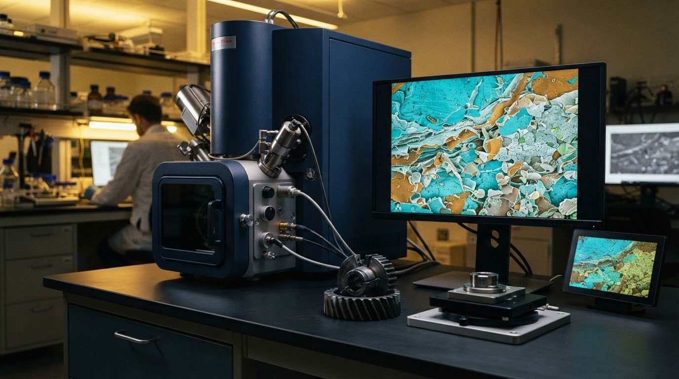
What can a microscopic image reveal about a product’s design, and what can’t it prove? Reverse engineering products with sem can uncover fine surface features and structural details that are difficult to assess at larger scales. But an image alone is not a complete product specification. Its value depends on how observations connect to measurements, material evidence, and the question being investigated.
SEM provides a closer look at how a component is formed and where a feature may differ. The key is to distinguish visual evidence from dimensional measurements and compositional analysis, then use each appropriately. SEM imaging can guide an investigation, while calibrated measurements and techniques such as energy-dispersive spectroscopy (EDS) can help answer separate questions about dimensions and elemental composition.
This practical workflow explains where SEM fits alongside other inspection methods, how to interpret findings without overreaching, and how to build a defensible evidence base for product-level decisions. It also shows how to choose a useful next step based on the specimen and the information your investigation needs.
Key Takeaways
- Use reverse engineering products with sem to investigate microscopic surface features, not as a standalone route to a complete product model.
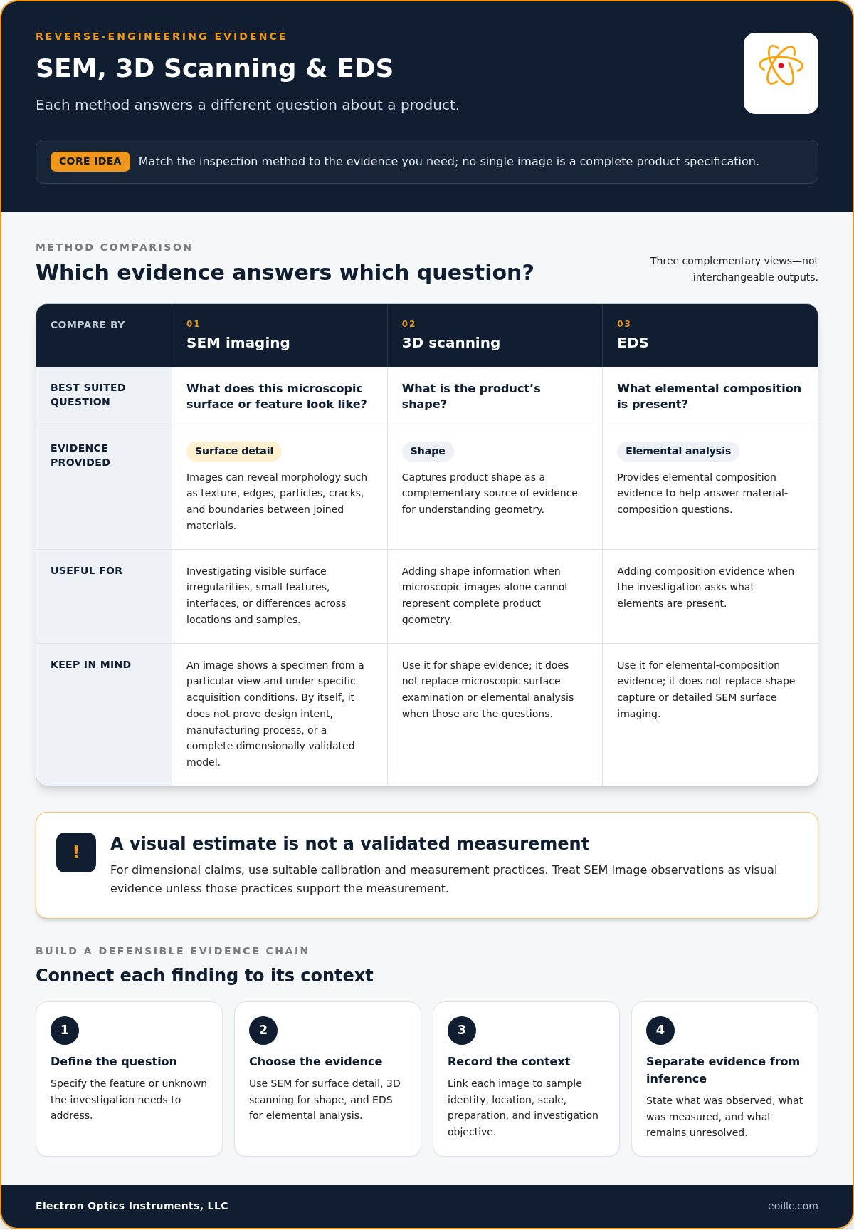
- Match each method to the question: SEM imaging reveals surface detail, 3D scanning captures shape, and EDS provides elemental analysis.
- Make findings easier to evaluate by linking each image to the sample identity, location, scale, and investigation objective.
- Separate direct observations and measurements from interpretations, and record unresolved questions before drawing product-level conclusions.
- Evaluate SEM equipment against your specimen and intended analysis. The Cube II SEM is specified at 5 nm resolution and magnification up to 300,000×.
What Does Reverse Engineering a Product with SEM Actually Reveal?
Reverse engineering starts with an existing object and uses evidence about its form, structure, and function to understand how it may have been designed or made, particularly when original drawings or specifications are limited. Reverse engineering spans many kinds of products and components. Scanning electron microscopy (SEM) adds a way to examine fine surface features at microscopic scale. For reverse engineering products with sem, distinguishing what an image shows from what an investigator infers is fundamental.
An SEM image can reveal surface morphology, including texture, edges, particles, cracks, and boundaries between joined materials. These observations can direct an investigation, but they don’t establish design intent or the manufacturing process by themselves. A visible groove, for example, is evidence of a surface feature. Concluding that it was machined, molded, or formed another way requires additional context.
SEM evidence can inform a CAD model, but an image does not automatically produce a complete, dimensionally validated model. Images show a specimen from a particular view and under specific acquisition conditions. Building product-level geometry may require measurements from other methods, information about the component’s function, and observations from additional locations or exposed cross-sections.
Which product questions can SEM help investigate?
Start with a question that can be answered by examining a particular surface or feature. Depending on the specimen and imaging conditions, SEM may help investigate:
- Whether a material surface shows pores, cracks, particles, wear, or other visible irregularities.
- How a small feature or interface appears on an electronic component, such as a circuit region or material boundary.
- Whether surface features differ across locations on a manufactured component or between samples.
Comparisons can sharpen the inquiry. An intact component, a failed part, and a differently processed sample may show contrasting features that point to areas for further analysis. The comparison is most useful when the samples are relevant to the same question and their preparation and imaging context are documented. A difference in appearance can guide an investigation, but it isn’t proof of the cause.
What SEM images cannot establish on their own
An image records visible surface evidence, not every internal feature or the complete three-dimensional form of a product. A cross-section can expose internal structure for examination, but it represents a prepared cut through the specimen, not a full model. Apparent feature size and contrast also depend on image scale and acquisition conditions. Treat a visual estimate as an observation, not a validated measurement, unless suitable calibration and measurement practices support it.
Build conclusions from traceable evidence: identify the sample and region, retain the scale and imaging context, and distinguish observation from interpretation. Repeat observations across relevant areas or samples, then add complementary evidence when the question concerns hidden geometry, dimensions, or composition. This keeps microscopic findings useful without asking them to support claims they cannot establish.
How to Use SEM Evidence in a Product Reverse-Engineering Workflow
A reliable investigation begins with the decision the evidence needs to support, not with collecting images at the highest available magnification. In reverse engineering products with sem, a defined question helps focus sample selection, imaging, and follow-up analysis. It also makes it easier to separate what the SEM directly shows from the measurements and engineering assumptions used to interpret it.
Prepare the investigation around a specific question
Before imaging, identify the unknown feature, failure, interface, or manufacturing detail under study. Record the product’s known history and gather available drawings, specifications, and comparison samples. Identify representative regions that can answer the question, including relevant areas away from an apparent defect. Sample preparation depends on the material and investigation objective, so select it for the specimen rather than treating one approach as universal.
- Define the decision. State what you need to determine, such as whether a crack follows a material boundary or whether a small feature differs between samples. Keep the question specific enough to guide where and how you examine the specimen.
- Establish sample identity. Assign each object or section a consistent identifier. Record its condition, history, and relationship to any reference sample so later observations can be traced to the correct product or component.
- Select regions deliberately. Choose locations that represent the feature of interest, and record their position relative to the whole part. When comparing intact and failed components, include corresponding regions where practical. A single unusual location may not represent the product overall.
- Acquire and annotate images. Preserve the image scale, sample location, relevant acquisition conditions, and preparation details needed to interpret the view. Mark the feature being discussed without obscuring the original image or losing its identifying information.
- Validate before concluding. Compare repeat observations or suitable reference samples. Separate visible observations from measured outputs, interpretations, and assumptions about design or manufacture. Flag questions that require dimensional metrology, sectioning, or another analytical method.
Capture, annotate, and validate SEM observations
For each image, record enough context for another reviewer to understand what was examined and how the view relates to the product. Note the region, scale, specimen identity, and relevant imaging conditions. Describe features in neutral terms before proposing a cause. For instance, document an observed discontinuity as a surface crack, while treating its origin as a separate interpretation that needs supporting evidence.
“An SEM image is only as defensible as the sample identity, location, scale, and acquisition context recorded with it.” This documentation lets reviewers distinguish image evidence from a dimensional measurement or an engineering hypothesis. When a decision depends on an actual dimension, internal geometry, or material composition, record that as a separate evidence need rather than inferring it from appearance.
When selecting an instrument around the specimen and intended analysis, explore SEM equipment and support as a practical next step.
SEM, 3D Scanning, and EDS: Which Evidence Answers Which Question?
Choose an inspection method based on the evidence the engineering question requires. SEM, three-dimensional scanning, and energy dispersive spectroscopy (EDS) address different aspects of a specimen, so their outputs aren’t interchangeable. For reverse engineering products with sem, SEM can reveal small-scale surface morphology, 3D scanning may capture broader external form, and EDS can support elemental-composition analysis.
| Method | Evidence produced | Suitable question | Limitation |
|---|---|---|---|
| SEM imaging | Images of surface features and morphology at microscopic scale | What does a small feature, surface defect, or interface look like? | Images show selected views, not a complete external or internal three-dimensional model. |
| 3D scanning | Digital information representing external shape, with output dependent on system capability | What is the broader external geometry of an accessible component? | Results depend on the scanner, specimen, and workflow. A scan doesn’t by itself reveal fine microscopic surface structure or composition. |
| EDS | Elemental-analysis evidence associated with the examined sample region | Which elements are present in a region being investigated? | Elemental findings aren’t a complete material formulation, and EDS doesn’t provide a geometry model. |
SEM imaging versus 3D scanning
SEM is appropriate when the question concerns details such as a small crack, surface texture, particle, or material boundary. A 3D scanner serves a different purpose: capturing external shape at a broader component scale, within the limits of the system and scanning setup. Its output may support a digital shape representation, but it doesn’t replace close examination of microscopic features.
SEM evidence examines small-scale surface features; 3D scanning evidence represents broader external shape. Combining the two can connect an area of interest to the wider component: use scanning to represent the overall form, then SEM to inspect a selected feature. The value of that combination depends on the part, the systems used, and whether the resulting evidence answers the design question.
When EDS adds compositional evidence
EDS is useful when the investigation asks about elemental composition in a selected sample region, for example, whether a region contains elements that differ from an adjacent area. It adds compositional evidence alongside SEM imaging, but it doesn’t establish a complete recipe, material grade, or manufacturing history on its own. Interpret results in light of the specimen and the specific analytical question.
Electron Optics Instruments offers EDS systems for investigations that require elemental analysis. Select a method based on the evidence gap: SEM for surface detail, 3D scanning for broader external form, and EDS when elemental information is relevant. For a defensible product interpretation, tie each result to the question it can answer and identify where additional measurement or analysis is needed.
How to Turn SEM Findings into Defensible Product Insights
A useful SEM record lets another engineer understand not only what an image appears to show, but how that observation supports a product decision. In reverse engineering products with sem, this means maintaining a clear boundary between visual evidence, measured values, engineering interpretations, and unanswered questions. That distinction makes findings easier to review against drawings, reference parts, or measurements from other methods.
Build an evidence trail others can review
Use a consistent file-naming structure that connects each image to a sample and location, and preserve the original image alongside any annotated copy. Record who collected the observation and which product question it addresses. Keep notes concise but specific: an annotation can identify a visible edge or discontinuity, while the written interpretation should separately explain what that feature may mean.
For operational context, the guide to SEM operation can help explain the imaging process behind the evidence. Use a practical review checklist to keep records consistent:
- Observation: Describe visible features without assigning a cause.
- Measurement: Record any dimension as a measurement output, with the method and relevant scale or calibration context.
- Interpretation: State the engineering explanation as a hypothesis or conclusion, and identify the evidence supporting it.
- Open question: Note what remains unknown and what additional evidence could resolve it.
Each image should be traceable to the sample identity, the precise location examined, its scale, and the investigation objective. Compare observations with available drawings or reference parts, but note differences in sample condition or measurement method that could affect the comparison. Agreement may strengthen an interpretation; a mismatch is a reason to investigate further, not to silently adjust the record.
Know when to add another analytical method
SEM images may indicate where a feature needs closer attention, but a product decision may depend on evidence beyond image interpretation. If the unknown is a dimension, use suitable dimensional metrology. If it concerns elemental composition, consider a relevant compositional method. Sectioning may be needed to examine a feature beneath the surface, depending on the specimen and question. Choose the next method for the specific evidence gap, not simply because it is available.
Keep the reasoning explicit: identify what the SEM establishes, what other evidence contributes, and which assumptions still need validation. When an investigation extends beyond routine imaging, define the unresolved question and select the appropriate method to answer it.
To connect your investigation needs with suitable SEM equipment and related support, explore SEM solutions from EOI.
Choosing SEM Equipment and Support for Reverse-Engineering Work
Selecting an SEM for reverse engineering products with sem starts with the investigation, not a model name. Consider the specimen’s scale and material, the features you need to examine, whether imaging alone is sufficient, how often the instrument will be used, and the practical constraints of the laboratory. This framework connects instrument capabilities and workflow requirements to the evidence your engineering decisions depend on.
Relate the investigation to EOI’s SEM range
EOI’s range includes the Cube II SEM, Genesis SEM, and Veritas SEM. The Cube II is a tabletop SEM marketed as the smallest conventional SEM on the market today. Its specified resolution is 5 nm, with magnification up to 300,000×. These specifications apply to the Cube II and shouldn’t be assumed for other instruments in the range.
The Genesis SEM is a compact conventional SEM family. The Genesis-1000 and Genesis-1100 have a straightforward, intuitive manual stage; the Genesis-1100 supports observation of non-conductive samples. The Genesis-2020 and Genesis-2120 provide a more versatile 5-axis motorized stage, with that stage specified for the Genesis-2120. The Veritas SEM is optimized for high-throughput quality-control sample analysis and requires no complex utilities for operation. To compare options, define the specimen, the scale of features involved, and whether your workflow calls for imaging, EDS, or both. Then consider how those needs align with laboratory conditions and intended use.
Plan for sustained operation and operator capability
Instrument fit also depends on the people and processes that support consistent use. Consider operator training, planned upkeep, and access to replacement parts as part of the workflow. EOI provides on-site SEM training, preventative maintenance service contracts, and replacement-parts support. Its factory-trained service engineers average over two decades of experience, and the service team is available 24/7/365. Service is required to keep SEM equipment operating at optimal specifications, and EOI provides service under contract.
EOI’s on-site training covers SEM operation, basic maintenance, and cleaning procedures. A defined maintenance plan can help laboratories organize instrument care alongside research and quality-control schedules.
Before evaluating a system, document the sample types, the questions operators need to answer, the frequency of imaging, and any complementary analysis requirements. These details give the selection process a practical basis instead of relying on magnification or resolution as isolated specifications. They also help clarify how training and service support contribute to effective laboratory operation over time.
For a focused discussion of SEM equipment and support for your investigation, connect with EOI’s SEM team.
Move Your Product Investigation Forward
Turn the investigation into a focused plan: identify the engineering decision at stake, define what evidence would support it, and decide how the findings will be used by the design or manufacturing team. This helps prevent image collection from becoming an end in itself and gives colleagues a clear basis for evaluating what is established and what still needs investigation.
For reverse engineering products with sem, progress depends on aligning the instrument and analytical approach with the specimen and the decision you need to make. A well-scoped application can help determine which SEM capabilities and supporting analysis are relevant to your workflow before you build the investigation around them.
Bring your sample type, research question, and intended use of the results into the discussion. Discuss your SEM application with Electron Optics Instruments and take a practical next step toward evidence that can inform your product decisions.
Frequently Asked Questions
Can an SEM create a complete 3D model of a product?
No. An SEM image records a view of an examined region, not the depth, hidden surfaces, or full geometry needed to define a complete product model. In reverse engineering products with sem, engineers may combine image evidence with external scans, dimensional measurements, and modeling. For example, a housing’s visible surface may be imaged, while concealed features require separate evidence. Keep each input traceable so the model’s basis and limitations remain clear.
Can SEM reveal what a product is made of?
SEM imaging alone doesn’t provide complete material identification. If the investigation asks which elements are present in a particular area, EDS can add elemental-analysis evidence. For a coated component, results need to be interpreted in relation to the sampled region and the question being asked. Elemental findings don’t necessarily identify compounds, material grade, or the full formulation, so don’t treat them as a complete recipe.
Is SEM suitable for reverse engineering electronic products?
Yes. SEM can help examine exposed small-scale features on electronic components, such as a contact surface or an interface. A useful question might be whether a visible area differs between a functioning part and one with a suspected defect. Access and sample condition matter: an external view can’t establish the structure of a feature that remains covered. Additional analysis may be needed for dimensions, internal features, or elemental information.
What happens if the product feature is inside a component?
An SEM can’t image an internal feature through an intact, opaque component. The investigation may need a prepared cross-section that exposes the region, or another method suited to the feature and specimen. Before preparation, record the component’s orientation and identify the area of interest. This helps preserve the relationship between the exposed section and the whole part. A single section represents one cut location, not the complete internal design.
How do SEM findings support product redesign?
SEM findings can inform redesign by helping engineers identify a surface feature or difference that merits attention, but they shouldn’t dictate a design change in isolation. A team might compare an observed feature with the drawing, a reference part, and relevant functional requirements before deciding whether a revision is justified. Record which evidence supports the decision and which assumptions remain, so design reviews can assess the reasoning rather than relying on an image alone.
Can EDS replace SEM imaging in reverse engineering?
No. EDS and SEM imaging answer different questions. SEM images show the appearance and morphology of the examined surface, while EDS adds evidence about elemental composition in a selected region. For example, an image may locate a feature of interest, while EDS analysis can help investigate its elemental content. Neither method supplies all product information: EDS doesn’t define complete geometry, and an image doesn’t establish a complete material formulation.