

The transition from qualitative topographical imaging to rigorous, quantitative material characterization represents the most significant shift in laboratory standards for 2026. Achieving sub-nanometer resolution requires more than just advanced hardware; it demands a sophisticated approach to sem operation that balances vacuum stability with precise electron optical calibration. You’ve likely experienced the technical hurdles of inconsistent image quality or the operational setbacks caused by improper filament handling, which can jeopardize critical research timelines and increase equipment wear. This professional guide provides the technical framework necessary to master these nuances, ensuring your laboratory achieves publication-quality imaging and reliable analytical data across all professional environments. We’ll examine the implementation of the ISO 25387:2026 protocol for performance validation, the integration of AI-driven automation for parameter optimization, and standardized handling protocols designed to reduce downtime and maximize the longevity of your Veritas or Cube II systems.
Key Takeaways
- Establish a technical foundation in vacuum integrity and electron source management to ensure a stable environment for high-precision imaging.
- Refine your sem operation by calibrating accelerating voltage and probe current to achieve the optimal balance between resolution and signal-to-noise ratio.
- Adopt standardized sample preparation workflows, including advanced mounting and sputter coating techniques, to facilitate consistent and reliable analytical results.
- Identify the strategic advantages of professional on-site training in reducing operational errors and maximizing the long-term ROI of advanced hardware systems.
The Fundamentals of Professional SEM Operation
Professional sem operation is characterized by the meticulous management of the interaction between a finely focused electron beam and the specimen surface. This process is not merely a sequence of button presses but a sophisticated synergy between hardware precision and the operator’s ability to interpret complex software interfaces. As we move through 2026, the industrial demand for rapid, high-resolution data has shifted the baseline of operational standards. Modern protocols prioritize instruments that offer both high-performance imaging and streamlined workflows, allowing laboratories to maintain high throughput without compromising on the meticulous accuracy required for failure analysis or material characterization. Understanding the fundamental signal types is essential for this level of precision; Secondary Electrons (SE) provide the high-resolution topographical details necessary for surface analysis, while Backscattered Electrons (BSE) offer critical compositional contrast based on atomic weight variations.
The Core Mechanism: From Electron Source to Detector
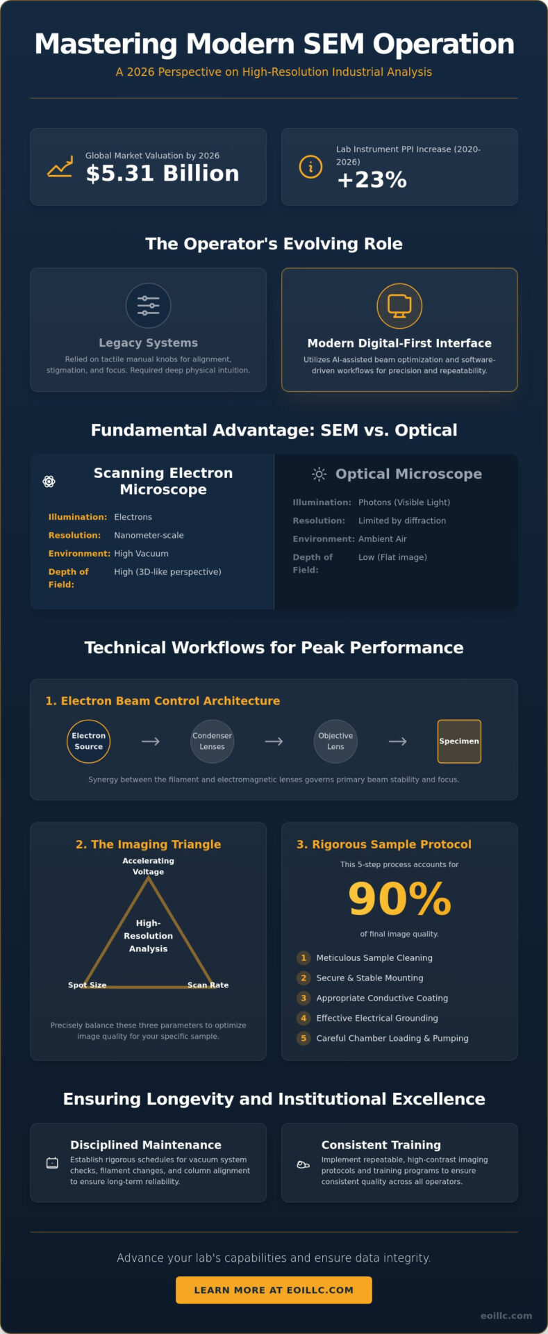
The foundational physics of a Scanning Electron Microscope begin within the electron optical column, where a primary electron beam is generated from a source, typically a Tungsten filament or a Field Emission gun. This beam is accelerated and focused through a series of electromagnetic lenses before it reaches the specimen. The scanning coils then manipulate the beam in a precise raster pattern across the surface. As the electrons strike the sample, various signals are emitted and captured by specialized detectors. These signals are subsequently converted into a digital representation, producing the high-resolution topography that defines modern microscopy. The operator must master this conversion process to ensure that the resulting digital data is a faithful and precise representation of the physical specimen. It’s a delicate balance of physics and digital signal processing that requires a deep understanding of electron-matter interactions.
Distinguishing Benchtop vs. Floor Model Workflows
The evolution of hardware has led to a significant divergence in operational workflows between traditional floor models and advanced benchtop systems. The Cube II Benchtop SEM represents the pinnacle of this shift, offering industrial-grade resolution within a compact footprint that significantly reduces the complexity of sem operation. Unlike larger floor-standing units that often require extensive vacuum stabilization periods and specialized facility requirements, benchtop systems offer rapid startup times and simplified loading procedures. Integrating desktop SEM technology into high-throughput research environments allows for immediate data acquisition without the logistical bottlenecks associated with centralized core facilities. This accessibility doesn’t come at the cost of performance; systems like the Veritas series bridge the gap, providing the sub-nanometer resolution typically reserved for larger installations while maintaining the efficiency required for modern industrial timelines. Choosing the right scale depends on your specific volume requirements and the physical constraints of your laboratory environment.
Managing the Vacuum System and Electron Source
The invisible architecture of any successful sem operation rests upon the stability of its vacuum environment. Maintaining a high-vacuum state is not merely a technical requirement but a critical necessity to prevent electron scattering and mitigate the risk of sample contamination. When gas molecules remain within the column, they intercept the primary electron beam, which leads to a significant reduction in signal intensity and image clarity. In high-volume industrial environments, the accumulation of hydrocarbons can lead to carbon deposition on the specimen, a phenomenon that obscures fine topographical details and compromises analytical integrity. Professional operators must prioritize the monitoring of vacuum levels as a primary diagnostic tool to ensure long-term system stability and reproducible data acquisition.
Vacuum Pump Technology and Chamber Integrity
Operational vacuum is typically achieved through a multi-stage pumping system, where a rotary vane or dry scroll pump provides the initial roughing vacuum, followed by a turbo-molecular pump that reaches the high-vacuum levels required for imaging. Safely venting and evacuating the specimen chamber requires a methodical approach; rapid pressure changes can disturb delicate samples or introduce atmospheric moisture that prolongs subsequent pump-down cycles. Identifying signs of vacuum leaks or pump degradation is a core competency of a seasoned operator. An unexpected increase in evacuation time or the inability to reach the base pressure often indicates a failing O-ring or a compromised seal. Regular inspection of chamber seals and the use of high-quality SEM consumables are essential practices for maintaining the integrity of the system.
Filament Handling and Saturation Protocols
The lifecycle of an electron source is heavily influenced by how it’s managed during the startup and shutdown phases. For Tungsten filaments, the saturation protocol is vital. This involves gradually increasing the heating current until the emission reaches a plateau, which maximizes brightness while preserving the structural integrity of the filament wire. Over-saturation leads to premature breakage, while under-saturation results in insufficient beam current and poor signal-to-noise ratios. Operational differences become more pronounced when utilizing a field emission scanning electron microscope for nanometer-scale resolution. FE sources, such as those found in the Veritas FE series, require ultra-high vacuum environments and different flashing protocols to maintain the sharpness of the emitter tip. Monitoring the emission current stability acts as a predictive marker for source exhaustion, allowing laboratories to schedule maintenance before a catastrophic failure occurs. Integrating these protocols into your daily sem operation ensures that systems like the Cube II or Veritas Pro maintain peak performance throughout their service life.
Optimizing Imaging Parameters for High-Resolution Data
Precise imaging is contingent upon the meticulous calibration of several interdependent variables, where the operator must balance theoretical resolution against the practical realities of specimen interaction. While higher accelerating voltages (kV) theoretically enhance resolution by shortening the electron wavelength, professional sem operation in 2026 requires a more nuanced understanding of beam penetration. Excessive voltage often leads to an increased interaction volume, which can obscure fine surface details or induce thermal damage in beam-sensitive materials. Conversely, lower kV settings are essential for capturing true surface topography and mitigating subsurface charging, particularly when analyzing polymers or biological specimens that lack a conductive coating.
Managing the relationship between spot size and probe current is equally vital for achieving publication-quality results. A reduced spot size minimizes the area of electron impact, providing superior clarity at high magnifications, yet this reduction inevitably lowers the signal reaching the detector. To compensate, operators must extend dwell times or adjust detector gain to maintain an acceptable signal-to-noise ratio. Furthermore, the working distance (WD) acts as a pivot point between resolution and depth of field; a shorter WD is preferred for ultra-high-resolution surface analysis, while a longer WD provides the depth necessary for imaging complex, three-dimensional structures. Throughout this process, the use of stigmation controls is non-negotiable to correct beam asymmetry, ensuring that edges remain crisp and free from the directional blurring caused by electromagnetic astigmatism.
Contrast and Brightness: Beyond Visual Aesthetics
Detector gain and offset must be adjusted with technical precision to preserve the full dynamic range of topographical detail without saturating the signal. On non-conductive samples, the phenomenon of “charging” acts as a significant barrier to stable imaging, often manifesting as bright flares or unpredictable image shifts. These effects are best mitigated through parameter adjustment, such as lowering the probe current or utilizing the software-driven auto-optimization tools integrated into modern systems like the Veritas series. These automated routines facilitate rapid calibration, allowing the operator to focus on the interpretation of data rather than the repetitive correction of hardware fluctuations.
Analytical Integration: Energy Dispersive Spectroscopy (EDS)
Achieving reliable elemental data requires that the sem scanning electron microscope be properly calibrated for simultaneous imaging and microanalysis. This integration demands specific operational requirements, such as optimizing the takeoff angle and managing detector dead time. Dead time, the period during which the detector is unable to process incoming X-rays, must be kept within a specific range to ensure spectral accuracy. High probe currents are often necessary to generate sufficient X-ray counts for rapid mapping, but they must be balanced against the risk of detector saturation, which can introduce artifacts and compromise the quantitative integrity of the analytical data during sem operation.
Professional Workflow: Sample Preparation and Loading
High-resolution imaging is fundamentally limited by the quality of the specimen interface. In a professional sem operation, the preparation phase is a rigorous technical procedure designed to ensure that the specimen is compatible with the ultra-high vacuum environment and the primary electron beam. Failure to address sample volatility or conductivity results in the immediate degradation of the analytical environment, potentially leading to the contamination of the electron optical column described in previous sections. The selection of a mounting substrate must be dictated by the material’s mechanical properties; for instance, metallic stubs provide the necessary stability for heavy industrial samples, while specialized carbon tapes or conductive epoxies are required for delicate powders and cross-sections.
Managing the phenomenon of outgassing is a critical responsibility for the operator. Porous materials, polymers, and biological specimens often harbor moisture or volatiles that, when exposed to high vacuum, can cause sudden pressure spikes. These fluctuations not only compromise image stability but also place undue stress on the turbo-molecular pumps. Professional protocols necessitate thorough desiccation or critical point drying before the sample enters the chamber. This methodical approach ensures that the vacuum integrity is maintained, protecting the longevity of your electron source and preventing the accumulation of hydrocarbons on sensitive detectors.
Conductive Coating and Mounting Techniques
The application of a conductive layer is often necessary to facilitate the dissipation of incident electrons. The choice between carbon and metallic coatings, such as gold or platinum, depends on the specific research objectives. Gold provides superior secondary electron yield for high-contrast topographical imaging, whereas carbon is the preferred medium for Energy Dispersive Spectroscopy (EDS) because its low atomic number minimizes spectral interference. Establishing a reliable Ohmic contact between the specimen surface and the ground is essential to facilitate the continuous dissipation of incident electrons and eliminate the deleterious effects of specimen charging during operation. Ensuring mechanical stability on the SEM stub is equally vital; any microscopic vibration can manifest as artifacts that obscure the sub-nanometer features captured by systems like the Veritas Ultra.
The Specimen Loading Sequence
The loading sequence must be executed with precision to avoid catastrophic damage to the internal hardware. A pre-loading inspection ensures that samples are dry and free of loose particulate that could be drawn into the vacuum system. Once the specimen is secured on the stage, the operator must navigate the X, Y, and Z axes with caution. Setting the Z-height limits is the most critical safety protocol in sem operation. A collision between the sample and the final lens pole piece can result in irreversible damage to the electromagnetic lens system. To maintain the precision of your instrument’s internal mechanics and ensure all stage movements remain calibrated, it’s advisable to schedule regular Preventative Maintenance Visits with an authorized service provider.
Elevating Lab Performance with Specialized SEM Training
The technical mastery of the electron optical column is only fully realized through the proficiency of the laboratory staff. Professional sem operation in 2026 requires a sophisticated understanding of both hardware physics and software-driven automation, a balance that is best achieved through structured, on-site instruction. Investing in specialized training yields a significant return on investment by drastically reducing the frequency of operator-induced errors and maximizing instrument uptime. These training modules are most effective when customized for specific industrial applications, whether the laboratory’s primary focus is failure analysis, material characterization, or high-throughput quality control. By aligning personnel capabilities with the advanced features of the Veritas or Genesis series, organizations ensure that their data remains both accurate and reproducible across long-term research cycles.
Standardizing Lab Protocols through Expert Instruction
Standardization is the cornerstone of reliability in professional microscopy. Developing Standard Operating Procedures (SOPs) tailored to specific hardware, such as the Cube II benchtop system, allows for a seamless transition of responsibilities among laboratory staff. Expert instruction facilitates the creation of these rigorous protocols, ensuring that every user maintains the same high standards for vacuum management and beam calibration. For senior staff, advanced troubleshooting modules provide the expertise needed to identify subtle system fluctuations before they impact data integrity. This level of technical depth is essential for maintaining regulatory compliance in sectors where meticulous documentation and precision are non-negotiable requirements.
The Synergy of Operation and Preventative Maintenance
Peak performance is maintained through the continuous synergy between daily operational discipline and professional technical support. Integrating sem maintenance training into the daily routine empowers operators to perform essential checks, such as monitoring emission stability and verifying vacuum pump efficiency. These daily and monthly assessments act as an early warning system, allowing for proactive adjustments that prevent the necessity of reactive, costly repairs. Transitioning to a proactive operational strategy is further supported by tiered service agreements that include regular professional service intervals for column cleaning and vacuum system overhaul.
Electron Optics Instruments, LLC supports this commitment to laboratory excellence through comprehensive service contracts and authorized technical support. By combining 30 years of industry expertise with a visionary approach to hardware longevity, we ensure that your sem operation remains at the forefront of industrial innovation. Our role as a reliable partner extends beyond the initial installation, providing the steady, expert-driven narrative your team needs to push the boundaries of what is possible in advanced material science and logistical excellence.
Achieving Operational Excellence in Modern Electron Microscopy
The transition toward sub-nanometer resolution in 2026 demands a rigorous commitment to technical precision. Mastering sem operation involves more than just software familiarity; it requires a deep integration of vacuum stability, electron optical calibration, and standardized sample preparation workflows. By implementing the professional protocols outlined in this guide, your laboratory can achieve the consistent, high-resolution data necessary for advanced material characterization while minimizing the operational downtime that often results from improper handling. These standards ensure that your research remains reliable and reproducible in an increasingly demanding industrial landscape.
Electron Optics Instruments, LLC provides the technical authority and logistical excellence required to maintain these high standards. With over 30 years of industry expertise and our status as the sole US distributor for EmCraft Benchtop SEMs, we offer a level of reliability that’s unmatched in the sector. Our comprehensive service contracts for all major SEM brands ensure that your hardware remains a precise instrument of innovation. Explore our on-site SEM training and technical support services to elevate your team’s proficiency and protect your institutional investment. We’re ready to partner with you in pushing the boundaries of what’s possible in professional microscopy.
Frequently Asked Questions
What are the basic steps for starting up a scanning electron microscope?
The initiation of a scanning electron microscope session requires a methodical sequence that prioritizes system integrity and vacuum stability. Operators must first verify the functionality of the roughing and turbo-molecular pumps to ensure the chamber reaches its operational vacuum threshold. Once the specimen is loaded and the chamber is re-evacuated, the electron source is gradually energized to its saturation point, followed by the meticulous alignment of the primary beam within the optical column.
How does accelerating voltage affect SEM image resolution and sample interaction?
Accelerating voltage, measured in kilovolts (kV), determines the energy level of the primary electron beam, directly influencing both the point resolution and the depth of the interaction volume. While higher voltages provide superior resolution for dense materials, they also increase beam penetration; this can obscure fine surface features and induce thermal damage in sensitive specimens. Professional operators often utilize lower voltages to capture true surface topography and mitigate subsurface charging effects.
Why is a vacuum necessary for scanning electron microscope operation?
Maintaining an ultra-high vacuum is essential for sem operation to eliminate the presence of gas molecules that would otherwise intercept and scatter the primary electron beam. This vacuum stability ensures that the electrons reach the specimen surface with their intended energy and focus. Furthermore, a clean vacuum environment is critical to prevent the rapid oxidation of the electron source and to mitigate the deposition of hydrocarbons that can obscure fine topographical details during high-resolution imaging.
What is the difference between secondary electron and backscattered electron imaging?
Secondary electron (SE) imaging primarily captures low-energy electrons emitted from the specimen surface, which provides the high-resolution topographical data necessary for surface analysis. In contrast, backscattered electron (BSE) imaging utilizes high-energy electrons that are reflected by the sample. The intensity of the BSE signal correlates directly with the atomic number of the elements present, offering critical compositional contrast that allows for the visual differentiation of diverse material phases within a specimen.
How often should SEM filaments be replaced during normal operation?
The replacement interval for SEM filaments depends heavily on the source type and the rigorousness of the laboratory protocols. Standard Tungsten filaments typically offer a service life of 40 to 100 hours of active beam time, depending on the saturation levels maintained by the operator. High-performance Field Emission (FE) sources, such as those found in the Veritas series, can operate for several years under ultra-high vacuum conditions before requiring refurbishment or replacement.
Can I operate an SEM without sputter coating my samples?
Conductive coatings are not strictly mandatory for all specimens, but they are essential for achieving stable sem operation on non-conductive materials. While naturally conductive metals or semiconductors can be imaged directly, insulating samples often require a thin layer of gold or carbon to facilitate electron dissipation. In modern laboratories, low-voltage imaging or environmental modes are sometimes employed to observe uncoated specimens, though these techniques often involve a trade-off in point resolution compared to traditional sputter-coated workflows.
What is stigmation and how do I correct it during imaging?
Stigmation refers to the correction of electromagnetic astigmatism, a condition where the electron beam becomes elliptical rather than perfectly circular. This condition manifests as directional stretching or blurring in the final image, particularly at high magnifications. To correct this, the operator utilizes specialized stigmator controls to adjust the electromagnetic fields in the X and Y axes, ensuring the beam focus remains uniform across the entire raster pattern to achieve maximum clarity and edge definition.