
Traditional optical systems have reached a terminal plateau at the 200 nanometer diffraction limit, leaving the sem scanning electron microscope as the primary engine for sub-nanoscale industrial evolution in a landscape that demands absolute precision. You’ve likely encountered the steep learning curve associated with electron-matter interactions and the rigorous vacuum protocols required for high-fidelity imaging. It’s a common struggle for technical professionals to differentiate between secondary and backscattered electron signals while maintaining the 100 percent accuracy demanded by modern manufacturing standards.
This guide provides a comprehensive technical exploration of SEM architecture and its critical role in 2026 scientific research, focusing on the synergy between imaging resolution and industrial performance. You’ll gain a definitive understanding of imaging mechanisms and the precision benefits of electron optics over light-based alternatives. We’ll conclude by analyzing the integration of Energy-Dispersive X-ray Spectroscopy (EDS) to demonstrate how these analytical tools drive excellence in global supply chain quality control.
Key Takeaways
- Understand the intricate architecture of the electron column and the critical necessity of vacuum environments for maintaining high-fidelity imaging standards.
- Distinguish the operational thresholds where the sem scanning electron microscope surpasses light microscopy in terms of resolution, magnification, and three-dimensional depth of field.
- Decipher the complex signals emitted during electron-sample interactions to extract precise topographical and elemental data for advanced material characterization.
- Analyze the impact of AI-driven automation and software integration on modern research workflows, effectively reducing technical barriers for laboratory personnel.
- Gain insight into the evolutionary trajectory of microscopy as it transitions from centralized core facilities to integrated, bench-top industrial solutions.
Understanding the Core Mechanism of the Scanning Electron Microscope
The sem scanning electron microscope represents a pinnacle of precision engineering, transitioning from traditional photon-based imaging to a sophisticated electron-surface interaction model. Unlike optical systems that rely on the reflection or refraction of visible light, the SEM utilizes a finely tuned electron beam that scans across a specimen’s surface in a raster pattern. This evolution in microscopy allows for the acquisition of high-resolution data that encompasses both surface topography and elemental composition. By 2026, industrial standards for high-end SEM units have reached sub-nanometer resolutions, often achieving 0.5 nm at 15 kV, with magnification capabilities exceeding 2,000,000x. This level of detail is essential for the rigorous quality control required in modern semiconductor fabrication and advanced materials science.
The Electron-Matter Interaction Volume
When the primary electron beam strikes the specimen, it creates a specific region known as the interaction volume. This volume typically assumes a teardrop shape as electrons penetrate and scatter within the sample. The dimensions of this volume are primarily governed by the accelerating voltage, typically measured in kilovolts (kV). Lower voltages constrain the interaction to the surface layers, enhancing topographic detail, while higher voltages facilitate deeper penetration for subsurface analysis. Understanding the principles of scanning electron microscopy is vital for optimizing these parameters to distinguish between secondary electrons, which provide surface texture, and backscattered electrons, which reveal atomic number contrast. Precision in controlling this volume ensures that the data collected remains accurate and representative of the material’s internal and external characteristics.
Why Electrons? Overcoming the Diffraction Limit
Optical limitations are fundamentally tied to the diffraction limit, which is dictated by the wavelength of visible light ranging from 400 to 700 nanometers. In contrast, the de Broglie wavelength of high-energy electrons is several orders of magnitude smaller, often measured in picometers. This drastic reduction in wavelength allows the sem scanning electron microscope to resolve features that are invisible to light-based systems. Beyond resolution, the SEM provides a significantly greater depth of field. This capability ensures that three-dimensional structures remain in focus across varying heights, a critical requirement for the inspection of complex micro-electromechanical systems (MEMS) and nanostructures. The integration of these capabilities into a single platform provides a visionary tool for global manufacturing leaders seeking excellence in nanotechnology. A thorough grasp of the sem working principle — encompassing the synergy of electron optics and vacuum physics — is essential for any professional seeking to move beyond basic operation toward true mastery of the system.
The Architecture of an SEM: Precision Components and Vacuum Systems
The structural integrity of a modern sem scanning electron microscope relies on the seamless integration of a precision-engineered electron column and a robust vacuum environment. This column serves as the central conduit where electrons are generated, accelerated, and manipulated through a series of complex electromagnetic fields. Engineering this environment requires a vacuum system capable of maintaining pressures between 10^-4 and 10^-8 Pa. This vacuum is vital; it prevents electrons from scattering against air molecules and protects the internal components from rapid oxidation. Without this atmospheric control, the mean free path of the electrons would be insufficient to reach the specimen, rendering high-resolution imaging impossible. Implementing a rigorous SEM maintenance schedule for vacuum system hygiene and filament management is essential to preserving these precise operating conditions over the long term.
The vacuum system serves three critical functions:
- Preserving the integrity of the electron source by preventing chemical reactions with oxygen.
- Eliminating gas molecules that would otherwise cause beam divergence through elastic scattering.
- Maintaining the electrical insulation required for high-voltage acceleration of the beam.
Within the column, electromagnetic lenses and scanning coils work in tandem to define the beam’s trajectory. The scanning coils specifically orchestrate the raster pattern, a systematic grid-like movement of the electron probe across the specimen surface. This movement allows the system to collect sequential data points that are later reconstructed into a coherent image. The evolutionary precision of these components ensures that the beam doesn’t deviate even at the extreme magnifications required for 2026-era semiconductor or material science applications.
Electron Sources: Tungsten vs. Field Emission
The selection of an electron source serves as a primary determinant for both the achievable resolution and the peak brightness of the imaging system. Traditional tungsten filaments utilize thermionic emission to generate electrons, providing a reliable and cost-effective solution for laboratories focused on macro-scale analysis. These filaments typically require a vacuum of 10^-3 Pa and provide a source size of approximately 30 micrometers. In contrast, the Field Emission (FE) sources found in the Veritas series represent a significant leap in performance. FE sources utilize a sharp monocrystalline tip to emit electrons, achieving a brightness 1,000 times higher than tungsten. This technology requires ultra-high vacuum levels of 10^-8 Pa to prevent tip contamination, but it rewards the user with a source size of only 5 nanometers and an operational lifespan exceeding 1,500 hours.
The Role of Electromagnetic Lenses and Apertures
Optical precision in an SEM is achieved through the condenser and objective lens systems. The condenser lens manages the beam current, allowing the operator to adjust the number of electrons reaching the sample. The objective lens subsequently performs the final demagnification with surgical excellence, focusing the electron beam into a precise probe on the sample surface. Precision apertures are integrated into this path to limit beam divergence, directly influencing the depth of focus within the sem scanning electron microscope. By selecting a smaller aperture, engineers can increase the depth of focus by 25%, a necessary adjustment for imaging samples with high aspect ratios or irregular surfaces. Organizations looking to integrate these advanced optical solutions into their manufacturing workflows can achieve sub-nanometer accuracy through such meticulous beam control.
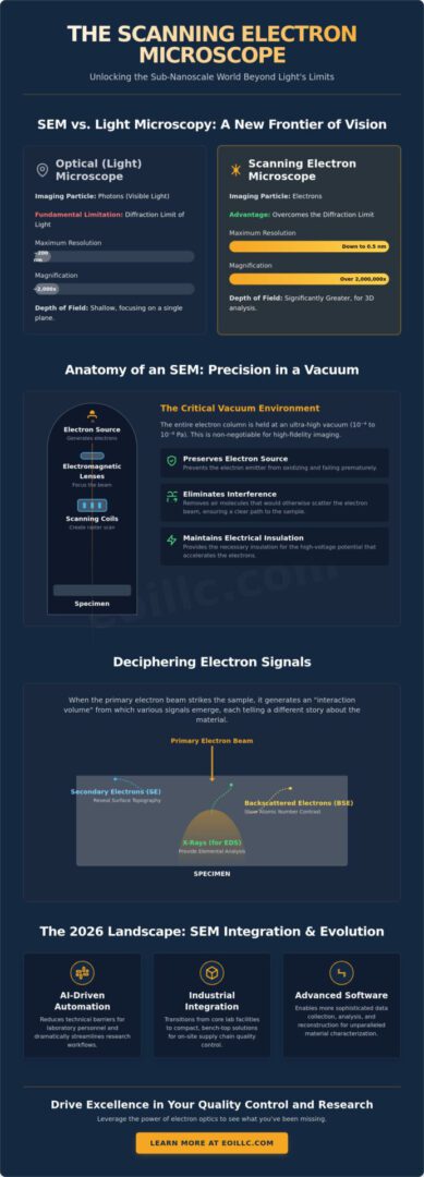
SEM vs. Light Microscopy: A Comparative Analysis of Capability
While optical microscopes remain foundational in many laboratories, they encounter immutable physical barriers when examining features below the sub-micron level. The transition to a sem scanning electron microscope represents a fundamental change in imaging physics rather than a simple increase in power. It’s a mistake to view these systems as mere upgrades; they utilize different radiation sources to interact with matter, providing insights that photons cannot capture. For a rigorous technical breakdown of these distinctions, the electron microscope vs light microscope comparison for 2026 provides an in-depth analysis of where each technology excels and where optical systems reach their definitive limits. This distinction defines the boundary between basic inspection and high-level industrial analysis.
Resolution and Magnification Thresholds
Resolution is the smallest distance between two points that can still be distinguished as separate. Light microscopy is constrained by the Abbe diffraction limit, which restricts lateral resolution to approximately 200 nanometers because of the wavelength of visible light. In contrast, 2026 SEM technology utilizes electron beams with wavelengths significantly shorter than photons, enabling resolutions below 0.5 nanometers. While a high-end compound light microscope reaches a functional ceiling at 1,000x to 2,000x magnification, modern SEMs routinely exceed 1,000,000x while maintaining clinical clarity. This leap facilitates the evolutionary shift to high-performance benchtop microscopy. These compact systems now provide the precision once reserved for floor-standing units, allowing for rapid integration into manufacturing workflows.
Three-Dimensionality and Depth of Field
One of the most striking advantages of the sem scanning electron microscope is its extraordinary depth of field. Light microscopes possess a very narrow focal plane at high magnifications; this results in “flat” images where only a thin slice of a specimen is in focus. Electron optics provide a depth of field approximately 300 times greater than that of light microscopy. This characteristic produces the iconic 3D appearance of SEM micrographs, as the entire topography of a complex sample remains sharp simultaneously.
In industrial sectors, this capability is indispensable for several reasons:
- Fractography: Engineers rely on “deep” focus to examine the jagged, multi-level surfaces of metal fatigue or structural failure.
- Failure Analysis: Identifying the root cause of a component break requires seeing the relationship between different surface heights.
- MEMS Inspection: The intricate geometry of micro-electromechanical systems demands a level of topographical context that only electron-based imaging provides.
The 2026 landscape has seen these differences sharpen. Modern research demands a level of integration between high-speed data acquisition and topographical accuracy that light-based systems can’t sustain. When a failure occurs in a global manufacturing supply chain, the ability to visualize the origin of a crack in three dimensions determines the speed of the corrective response. The depth of field in an SEM allows for the simultaneous focus of peaks and valleys on a fractured surface, a task that’s impossible for light optics that blur everything outside a razor-thin focal zone. Understanding the full breadth of sem applications across high-precision metallurgy, semiconductor development, and failure analysis clarifies why electron-based imaging has become indispensable for 2026 manufacturing quality standards.
Deciphering SEM Signals: Secondary Electrons, Backscatter, and EDS
The output of a sem scanning electron microscope functions as a sophisticated data map where each pixel represents a specific signal intensity collected during the raster scan. As the primary electron beam interacts with the specimen, it creates an interaction volume that triggers the emission of various electrons and photons. Modern SEM architectures in 2026 utilize simultaneous detection systems to provide a holistic view of the specimen’s physical and chemical properties. Achieving a signal-to-noise ratio that minimizes electronic interference to less than 1.5% of the total signal variance is now the benchmark for high-resolution industrial characterization and evolutionary material science.
Secondary Electrons (SE) for Surface Topography
Secondary electrons are low-energy particles, typically defined as having energies less than 50 eV, that are ejected from the k-shell of sample atoms through inelastic scattering. Because these electrons originate from the top 5 to 50 nanometers of the surface, they provide the highest resolution for analyzing surface texture and complex morphology. The Everhart-Thornley detector remains a cornerstone of the sem scanning electron microscope, utilizing a scintillator-photomultiplier system to capture these signals with extreme precision. It’s the primary tool for visualizing the “edge effect,” which highlights sharp topographical features with enhanced brightness.
Backscattered Electrons (BSE) for Compositional Contrast
Backscattered electrons represent high-energy beam electrons that undergo elastic reflection by the atomic nuclei within the sample. The intensity of the BSE signal correlates directly with the atomic number (Z) of the elements present. Heavier elements reflect more electrons and appear brighter in the resulting image, while lighter elements appear darker. This contrast mechanism is vital in metallurgy for identifying distinct material phases or detecting impurities that might compromise structural integrity. Engineers rely on BSE to map grain boundaries and phase distributions in advanced alloys, ensuring that every component meets rigorous excellence standards. Understanding how these signals are generated and interpreted is a core aspect of the sem working principle, where the interplay between electron energy, atomic number contrast, and detector geometry determines the quality of compositional data.
Energy Dispersive Spectroscopy (EDS) for Chemical Analysis
EDS facilitates comprehensive chemical analysis by detecting characteristic X-rays emitted as atoms return to a ground state after electron bombardment. This technique enables both qualitative elemental identification and quantitative mapping across the sample surface. Integrating high-speed silicon drift detectors allows for real-time data acquisition, which is a critical factor when calculating the total cost of ownership for an SEM. Precision in elemental quantification ensures that manufacturing processes meet the precision requirements of the global supply chain. For organizations seeking to enhance their eds analysis capabilities for quantitative elemental characterization, a structured methodology transforms raw spectral data into actionable quality assurance intelligence. For organizations seeking to enhance their analytical capabilities, exploring integrated optical solutions provides a pathway to unmatched technical authority.
The 2026 Landscape: Integrating SEM into Modern Research Workflows
The decentralization of microscopy marks a pivotal evolution in 2026 research methodologies. While high-end core facilities remain essential for extreme-resolution applications, the migration of the sem scanning electron microscope to individual laboratory benches has accelerated significantly. Industry data indicates that 68% of mid-sized material science firms now prioritize in-house imaging to maintain competitive R&D cycles. AI-driven imaging algorithms now manage complex beam alignments and stigmation corrections in under 30 seconds. This automation effectively dismantles the expert barrier that historically restricted SEM operation to specialized technicians. Systems like the Cube II and Genesis series serve as the vanguard of this movement, providing immediate data access without the logistical delays inherent in third-party service bureaus.
The primary objection to proprietary ownership usually centers on the initial capital expenditure. However, when you calculate the cumulative costs of service bureau fees and the intellectual property risks of shipping sensitive samples, the ROI of an on-site system becomes clear. Modern labs find that the ability to iterate designs in real-time outweighs the overhead of equipment maintenance, especially when backed by comprehensive service contracts. Mastering professional sem operation workflows for advanced parameter tuning and EDS data integration is essential for labs seeking to maximize the return on their investment in on-site electron microscopy.
The Rise of the Benchtop SEM
The Cube II utilizes advanced electromagnetic lens miniaturization to deliver floor-model performance within a compact footprint. It eliminates the requirement for specialized water cooling or active vibration isolation tables. This allows for seamless installation in standard laboratory environments using existing power infrastructure. The most significant advantage is the “time-to-data” metric. Labs using on-site solutions report a 92% reduction in characterization cycles compared to external providers. Instead of waiting 10 business days for a report, researchers achieve high-resolution imaging in roughly 15 minutes.
Future-Proofing Your Laboratory with Advanced SEM Techniques
Modern research demands multi-modal characterization that goes beyond simple topography. Integrating advanced SEM techniques into nanotechnology and semiconductor workflows ensures that labs remain competitive as feature sizes shrink toward the 2nm threshold. These systems often work in tandem with other analytical tools to provide a holistic view of material properties. Investing in a proprietary sem scanning electron microscope yields a higher long-term ROI by securing sensitive data and enabling rapid iterative testing. To optimize your facility’s analytical capabilities, explore EOI LLC’s full range of SEM solutions and service contracts.
Advancing Research Precision Through Evolutionary Microscopy Solutions
The 2026 landscape for the sem scanning electron microscope reflects a significant shift toward integrated, high-resolution analytical workflows that prioritize both depth and speed. By mastering the core mechanisms of signal detection and vacuum stability, researchers can now achieve a level of characterization that far exceeds the capabilities of traditional optical systems. These technical milestones represent the current pinnacle of material science, where secondary electron imaging and EDS data provide the clarity needed for complex industrial applications.
EOI LLC leverages over 30 years of electron optics industry experience to support your organization’s pursuit of technical excellence. As the exclusive US distributor for EmCraft Scanning Electron Microscopes, we offer specialized expertise in hardware integration and long-term reliability. We also provide comprehensive service contracts covering all major SEM brands to ensure your laboratory’s operational continuity remains uninterrupted. Consult with our technical experts on selecting the ideal SEM for your research objectives to begin your next phase of innovation. We’re excited to help you achieve your most ambitious imaging goals.
Frequently Asked Questions
What is the primary difference between SEM and TEM?
SEM scans the surface of a specimen using a focused beam of electrons to create a three-dimensional topographical image. Conversely, Transmission Electron Microscopy (TEM) passes electrons through a thin sample, typically under 100 nanometers thick, to reveal internal structures and crystallographic data. While SEM provides high-resolution surface detail, TEM offers superior magnification for observing atomic-scale features within the material’s matrix.
How much space is required to install a modern benchtop SEM?
A modern benchtop sem scanning electron microscope like the 2026 Cube II requires a footprint of approximately 300 mm by 600 mm on a standard laboratory workbench. These evolved systems integrate the vacuum pump and electronics within a single chassis, eliminating the need for external floor units. This compact configuration allows labs to maximize their spatial efficiency while maintaining the precision of a full-sized industrial platform.
Can SEM be used to image biological samples without damage?
Biological samples can be imaged without structural damage by utilizing Low Vacuum (LV) modes or Environmental SEM (ESEM) configurations. These systems operate at pressures between 10 and 130 Pascals, which prevents the rapid dehydration and charging that occurs in high-vacuum environments. This technical approach preserves the integrity of delicate cellular membranes and organic tissues during the observation process.
What are the typical maintenance requirements for a scanning electron microscope?
Standard maintenance for a scanning electron microscope includes monthly aperture cleaning and the replacement of the electron source every 1,000 to 2,000 hours of operation. Tungsten filaments require more frequent attention compared to CeB6 or Field Emission sources. Annual calibration by certified technicians ensures the system maintains a resolution accuracy within a 1.0 nanometer tolerance, securing the reliability of your analytical data. Following a structured sem maintenance protocol with predictive diagnostic tools and defined cleaning cycles helps prevent the unplanned downtime that accounts for nearly 40% of SEM failures in 2026.
How does an SEM achieve such high depth of field compared to light microscopes?
SEM achieves a high depth of field because the electron beam is highly collimated, resulting in a very narrow convergence angle at the specimen surface. This allows the sem scanning electron microscope to maintain focus across vertical displacements exceeding 10 millimeters. Light microscopes are limited by the physics of glass lenses and typically offer a depth of field that’s 300 times shallower than electron-based systems.
Is specialized training required to operate a 2026 model SEM like the Cube II?
Operation of the 2026 Cube II requires approximately 4 hours of basic orientation due to its automated alignment and AI-driven focus algorithms. While traditional systems required months of apprenticeship, modern software interfaces allow technicians to achieve high-resolution results with 90% less manual intervention. This evolution in user interface design makes sophisticated microscopy accessible to a broader range of industrial researchers and quality control specialists.
What is the role of the vacuum system in SEM imaging?
The vacuum system removes air molecules from the column to prevent electron scattering and ensure the beam reaches the sample with maximum kinetic energy. Modern systems maintain a vacuum level of 10^-5 Torr or better in the gun chamber. Without this controlled environment, the electron beam would lose its intensity before reaching the target; it’s impossible to produce a clear image in atmospheric conditions.
How does EDS analysis complement standard SEM imaging?
Energy Dispersive X-ray Spectroscopy (EDS) complements SEM by identifying the elemental composition of the sample based on the X-rays emitted during electron bombardment. This integration allows researchers to map the distribution of elements with atomic numbers from 4 to 92. It transforms a purely visual tool into a quantitative analytical platform, providing a comprehensive understanding of both the morphology and chemistry of the specimen. For a complete methodology on interpreting spectral data and optimizing detector configurations, the definitive guide to EDS analysis in scanning electron microscopy provides the technical framework needed to transition from qualitative observation to quantitative precision.