The traditional reliance on optical systems has reached a definitive physical threshold where the 200-nanometer diffraction limit now acts as a barrier to industrial progress rather than a benchmark for excellence. As we approach 2026, the debate regarding electron microscope vs light microscope utility is no longer about preference. It’s about whether your laboratory can afford to remain blind to the elemental and topographical realities of your materials. You’ve likely felt the constraints of optical tools when attempting to resolve sub-micron features or when your quality control requires chemical composition data that a lens simply cannot provide.
We understand that the transition from a standard light microscope to a scanning electron microscope often feels like a leap into unnecessary complexity or prohibitive spatial requirements. However, the evolutionary shift toward high-performance benchtop SEMs has dismantled these traditional barriers, offering a synergy of precision and accessibility. This technical comparison provides the rigorous evaluation framework you need to master the fundamental differences in physics and operational requirements. You’ll gain a clear understanding of resolution limits, including the jump to sub-nanometer imaging, and the ROI of modern microscopy solutions to ensure your facility maintains its competitive technical authority.
Key Takeaways
- Understand how the fundamental shift from visible photons to electron beams allows researchers to bypass traditional diffraction limits for superior imaging precision.
- Evaluate the technical divergence of the electron microscope vs light microscope regarding resolving power, ensuring your facility prioritizes detail extraction over hollow magnification metrics.
- Identify the specific environmental and vacuum requirements necessary to sustain high-precision imaging while demystifying the perceived complexities of modern SEM sample preparation.
- Determine the optimal transition point from traditional histology to advanced failure analysis by aligning your laboratory’s research objectives with specific sub-micron morphological capabilities.
- Explore how the evolutionary shift toward benchtop SEM solutions, such as the Cube II, integrates high-resolution performance with streamlined operational accessibility for modern industrial facilities.
Beyond Visible Light: The Fundamental Physics of Microscopy
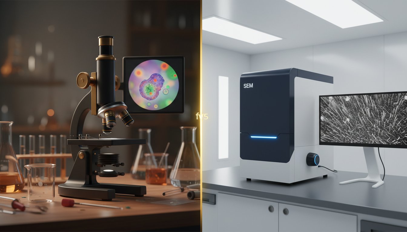
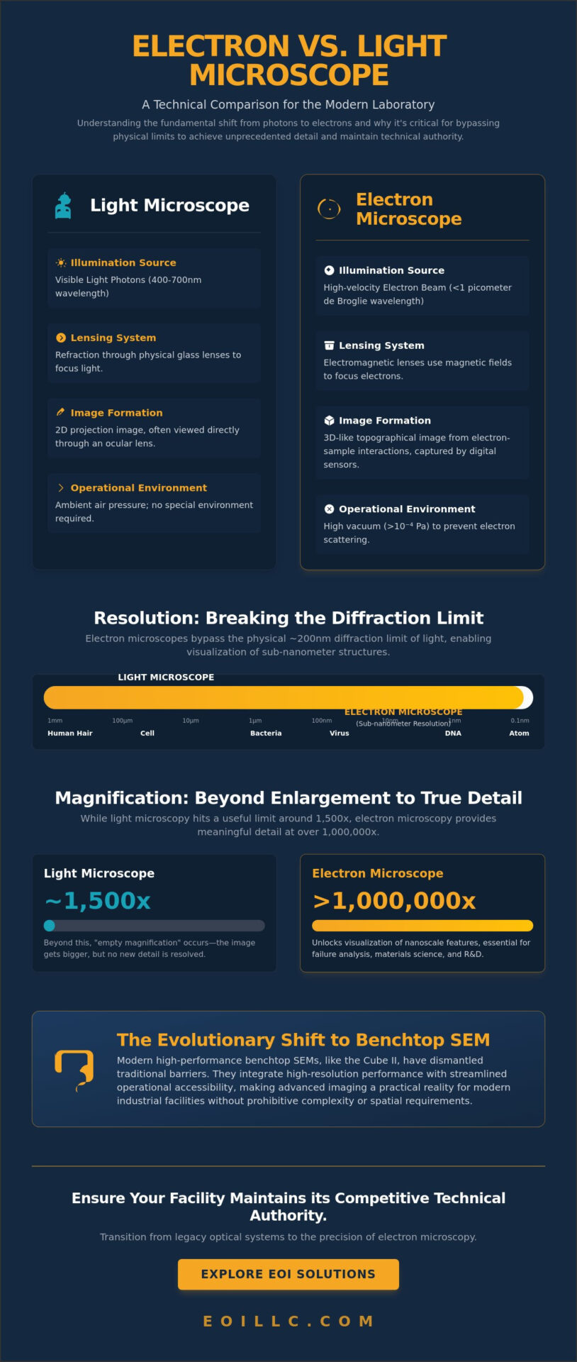
The primary divergence in the electron microscope vs light microscope debate begins with the physical nature of the radiation used to probe a specimen. While optical systems utilize photons within the visible spectrum, electron-based systems leverage high-velocity particles to bypass the inherent resolution constraints of light. This shift in the illuminating source represents an evolutionary leap in precision engineering, allowing researchers to visualize structures that were previously theoretical. The choice between these technologies dictates the level of detail extraction possible in modern laboratory environments.
The diffraction limit of visible light restricts optical resolution to approximately 200-250nm, preventing the visualization of structures smaller than half the wavelength of the light source.
To overcome this barrier, engineers utilize electromagnetic fields to guide subatomic particles. This technical transition from light to matter enables a level of magnification that is several orders of magnitude greater than traditional glass-based systems. The integration of these advanced physics principles ensures that industrial and scientific sectors can maintain the rigorous standards required for 2026 and beyond.
Illumination Sources and Wave Mechanics
The visible light spectrum, ranging from 400nm to 700nm, imposes rigid physical constraints on traditional microscopy. In contrast, this electron microscope overview details how de Broglie wavelengths, which can be less than 1 picometer at high acceleration voltages, allow for the extraction of atomic-level detail. Because electron beams are highly susceptible to atmospheric scattering, these systems operate within a vacuum environment maintained at pressures often exceeding 10^-4 Pa. This ensures the beam’s integrity remains uncompromised during its trajectory toward the sample, preventing the loss of resolution caused by collisions with gas molecules.
Lensing and Image Formation
Optical systems achieve magnification through the refraction of light within high-purity glass lenses. Electron microscopy replaces these physical barriers with electromagnetic lenses that utilize magnetic fields to deflect and focus the electron stream. This mechanism allows for a significantly higher depth of field; consequently, Scanning Electron Microscopes (SEM) provide a 3D-like perspective that flat light images cannot replicate. Modern systems have transitioned from direct ocular viewing to sophisticated digital sensor acquisition. These systems integrate CMOS or CCD technology to capture data with 4K or 8K resolution, ensuring that the precision of the raw signal translates into actionable industrial data for global manufacturing and quality control. For a deeper understanding of how these electromagnetic lenses and electron-sample interactions work together, the SEM working principle provides a rigorous technical breakdown of the hardware architecture that transforms electron signals into high-precision imaging data.
- Light Microscopy: Relies on photon refraction through convex glass.
- Electron Microscopy: Utilizes Lorentz forces within magnetic coils to converge electron paths.
- Digital Integration: High-speed sensors now replace the human eye to minimize user bias and enhance data repeatability.
Resolution and Magnification: Breaking the Diffraction Limit
Understanding the fundamental divergence in an electron microscope vs light microscope comparison requires a shift in focus from how large an image appears to how clearly it defines structural detail. While magnification describes the proportional enlargement of an object, it’s a hollow metric if the system cannot distinguish between two adjacent points. Optical systems are bound by the diffraction limit of visible light, which effectively caps useful magnification at 1,000x to 1,500x. Beyond this threshold, additional enlargement results in empty magnification; the image grows larger but lacks new detail, appearing blurred and indistinct. Conversely, electron microscopy leverages the significantly shorter wavelengths of electrons to achieve magnification levels ranging from 100,000x to over 1,000,000x in high-end units. This capability allows for the visualization of sub-cellular structures and atomic lattices that remain invisible to photons.
The Resolving Power Benchmark
Resolution represents the ability of an optical system to distinguish two closely spaced points as separate entities. In light microscopy, the resolution is mathematically limited to approximately 200nm due to the wavelength of light and the numerical aperture (NA) of the objective lenses. Physics dictates this boundary regardless of lens quality. In the context of 2026 nanotechnology and semiconductor inspection, a 200nm limit is insufficient for analyzing 5nm or 3nm process nodes. Electron microscopes overcome this physical barrier by achieving resolutions of 1nm or less. This precision is vital for industries where the decision between an electron microscope vs light microscope rests on the need to identify defects at the molecular level, ensuring that structural integrity meets global manufacturing standards.
Practical Magnification Limits
The distinction between useful and empty magnification defines the operational efficiency of a modern laboratory. Modern systems like the Cube II Benchtop SEM demonstrate how high-resolution imaging integrates into a compact footprint without sacrificing detector sensitivity. These units utilize advanced electron optics to provide clear, actionable data where traditional optics fail. By optimizing pixel size and signal-to-noise ratios, these benchtop solutions offer a bridge between basic inspection and high-end research. For organizations seeking to scale their analytical capabilities, investing in precision optical solutions ensures that magnification remains a functional tool for innovation rather than a decorative specification. The evolution of detector technology continues to refine these limits, making sub-nanometer analysis a standard requirement for industrial performance.
Operational Ecosystems: Vacuum Requirements and Sample Preparation
The historical barrier to adopting Scanning Electron Microscopy (SEM) often centers on the perceived complexity of the operational ecosystem. While a light microscope functions within standard atmospheric conditions, the electron microscope vs light microscope comparison reveals a fundamental divergence in environmental requirements. Traditional SEMs demand a high-vacuum state to prevent electron scattering by air molecules. However, the landscape in 2026 has shifted. Modern engineering has mitigated the learning curve. Current benchtop systems offer automated alignment and intuitive interfaces that rival the simplicity of high-end optical systems.
The Role of the Vacuum System
Electrons are highly sensitive to gas molecules. Without a vacuum, the primary beam would collide with nitrogen or oxygen particles, resulting in beam attenuation and significant image noise. Maintaining this environment requires sophisticated vacuum seals and turbo-molecular pumps. The Veritas Series SEM optimizes these pump-down cycles through advanced chamber geometry, reducing the transition from atmospheric pressure to high vacuum to under 90 seconds. For samples that are prone to outgassing or are non-conductive, Environmental SEM (ESEM) modes now allow for imaging at higher pressures, which preserves specimen integrity without sacrificing resolution. Understanding how vacuum levels directly impact image fidelity according to ISO 16700:2016 standards is a core component of mastering the sem working principle and the synergy between electron optics and vacuum physics that defines modern analytical excellence.
Sample Preparation Protocols
Sample preparation represents the most significant workflow difference when evaluating the electron microscope vs light microscope dynamic. Light microscopy facilitates rapid imaging of wet, live, or untreated specimens with minimal mounting. Conversely, SEM traditionally requires samples to be dry and electrically conductive. This often involves a multi-step protocol of chemical dehydration and sputter coating with gold or palladium. By 2026, the integration of low-vacuum detectors has revolutionized this process. Many industrial materials, such as polymers and ceramics, can now be imaged in their native state. This evolution reduces the total time-to-result from hours to approximately 5 to 10 minutes, making high-resolution analysis a viable component of high-throughput quality control lines.
- Light Microscopy: Atmospheric pressure operation; seconds to image; compatible with live-cell imaging.
- High Vacuum SEM: Requires 10^-3 to 10^-6 Torr; requires conductive coating; provides highest resolution.
- Environmental SEM: Operates at 1 to 20 Torr; images non-conductive samples without coating; balances speed and detail.
The choice between these systems depends on the required throughput and the physical nature of the specimen. While light microscopy remains the standard for rapid, live-tissue screening, the precision of modern SEM platforms provides a level of topographical detail that optical systems simply can’t match. As vacuum technology becomes more efficient, the operational gap between these two technologies continues to close, allowing researchers to move from sample loading to nanometer-scale visualization in a single, streamlined workflow.
Strategic Application: Choosing the Right Tool for Research and Industry
Determining the optimal instrumentation requires a rigorous evaluation of specific analytical objectives. Light microscopy maintains a dominant position in fields such as histology and routine metallurgical quality control. These applications rely on the natural color representation and high-speed throughput that optical systems provide. When an engineer needs to verify grain boundaries in a steel alloy at 500x magnification, the light microscope is the most efficient choice. It’s the standard for biological tissue staining where color differentiation is the primary diagnostic marker.
The technical transition to scanning electron microscopy becomes mandatory when the investigation shifts toward failure analysis or sub-micron morphology. In forensic science and advanced material engineering, the 200-nanometer diffraction limit of light becomes an insurmountable barrier. When comparing the electron microscope vs light microscope, the decision hinges on the required depth of field and resolution. SEM provides a three-dimensional perspective that’s impossible to achieve with photons, making it indispensable for analyzing fracture surfaces or complex nanostructures. For a detailed examination of how these capabilities translate across specialized sectors, our guide to SEM applications in industrial and research environments provides a comprehensive breakdown of real-world use cases and performance benchmarks.
Imaging vs. Analytical Composition
Optical systems are fundamentally limited to visual data. They can’t identify the elemental makeup of a sample. By integrating Energy Dispersive Spectroscopy (EDS), the SEM transforms from an imaging tool into a powerful chemical analyzer. This integration allows researchers to generate an elemental “fingerprint” of a sample. In semiconductor manufacturing, identifying a single sub-micron contaminant is vital for maintaining yield rates. EDS analysis can distinguish between a speck of aluminum and a fragment of silicon in seconds, a feat that’s beyond the capabilities of any light-based system. This distinction is a primary factor when evaluating the electron microscope vs light microscope for industrial quality assurance.
Financial and Spatial Considerations
The decision to upgrade involves a complex analysis of the electron microscope cost relative to the projected analytical value. While light microscopes require minimal infrastructure, electron-based systems demand controlled environments to mitigate vibration and electromagnetic interference. Modern engineering has led to the development of benchtop SEMs. These compact units offer a significantly smaller footprint than traditional floor-standing models while maintaining high-resolution capabilities. Long-term ROI is secured through comprehensive service contracts and preventative maintenance protocols that ensure 99% uptime in high-volume industrial environments. The investment reflects a commitment to precision that defines market leadership.
The Evolutionary Shift to Benchtop Scanning Electron Microscopy
The landscape of high-resolution imaging is undergoing a significant transformation as benchtop scanning electron microscopes (SEMs) become standard in mid-sized facilities. Historically, the choice in the electron microscope vs light microscope debate was dictated by physical space and massive capital expenditure. Today’s tabletop systems eliminate those barriers. The Cube II exemplifies this shift. It delivers 5-nanometer resolution and integrated Energy Dispersive X-ray Spectroscopy (EDS) in a footprint that fits on a standard laboratory bench. These systems democratize access to sub-micron analysis for organizations that previously relied solely on optical instruments.
The adoption of benchtop technology isn’t just about size; it’s about the precision of the data gathered. While a light microscope might reach its physical limit at 200 nanometers, the Cube II allows researchers to observe surface morphologies at much higher magnifications. This capability is essential for modern semiconductor and polymer research where feature sizes have shrunk beyond the reach of visible light. The integration of EDS allows for simultaneous elemental analysis, providing a chemical map of the sample that optical systems simply can’t replicate. For a comprehensive methodology on interpreting spectral data and maximizing elemental intelligence, our definitive guide to EDS analysis in scanning electron microscopy provides the rigorous technical framework required for modern quality assurance workflows.
Bridging the Gap with Tabletop Systems
The Genesis Tabletop SEM represents a departure from traditional floor models that require dedicated rooms and specialized cooling. While floor units offer ultimate magnification, the Genesis provides a user-friendly interface that allows technicians to produce publication-quality images without a PhD in physics. This accessibility facilitates the integration of electron optics directly into quality control workflows. By 2026, analysts expect that 40% of industrial material testing labs will utilize benchtop SEMs to augment their existing light microscopy capabilities. Refurbished SEM units also play a critical role. They offer a 30% to 50% reduction in entry costs for growing laboratories seeking to bridge the budget gap without sacrificing analytical precision.
EOI LLC: Your Partner in Analytical Excellence
EOI LLC serves as the primary US-based distributor for these advanced optical solutions, bringing over 30 years of technical expertise to the electron optics sector. We understand that purchasing capital equipment is a long-term commitment to precision. Our comprehensive service contracts include scheduled preventative maintenance and rapid-response repairs to ensure maximum uptime for your facility. Beyond the hardware, EOI LLC provides intensive on-site training. This ensures your team can fully exploit the capabilities of the electron microscope vs light microscope transition. Our legacy is built on providing the technical support necessary for sustainable industrial innovation and global manufacturing excellence.
- 30+ Years of Expertise: Deeply rooted in US distribution and technical support.
- Comprehensive Service: Contracts that cover both preventative maintenance and emergency repairs.
- Direct Training: On-site programs to maximize the utility of your capital investment.
Advancing Laboratory Standards Through Evolutionary Microscopy Solutions
The 2026 analytical landscape demands a rigorous understanding of the electron microscope vs light microscope dichotomy to ensure research integrity, particularly as the boundaries of nanotechnology continue to expand. While optical systems remain vital for observing live biological processes within the 200 nanometer diffraction limit, the integration of electron optics provides a resolution threshold reaching 1.0 nanometer. This technological leap allows for the detailed characterization of nanomaterials and semiconductor architectures that light-based systems simply can’t resolve. As industrial requirements shift toward high-throughput environments, the transition to benchtop scanning electron microscopy represents a critical evolutionary step in laboratory efficiency.
EOI LLC serves as the sole US distributor for EmCraft Scanning Electron Microscopes, bringing 30 years of industry-leading technical expertise to your facility. Our team provides full-service support for all major SEM brands; we ensure your equipment maintains peak precision throughout its operational lifecycle. It’s time to redefine your research parameters with sophisticated hardware designed for the next generation of discovery. Explore the Cube II Benchtop SEM and Upgrade Your Lab’s Capabilities Today. We look forward to supporting your journey toward scientific excellence.
Frequently Asked Questions
What is the main difference between an electron microscope and a light microscope?
The primary distinction between an electron microscope vs light microscope lies in the illumination source; light microscopes utilize photons and glass lenses, whereas electron microscopes employ accelerated electron beams and electromagnetic lenses. This fundamental shift in physics allows for a resolution limit of 0.1 nanometers in modern transmission electron microscopes compared to the 200 nanometer limit of optical systems. Engineers select these tools based on the specific architectural requirements of the specimen under analysis.
Can you see live cells in an electron microscope?
You can’t observe live biological specimens in an electron microscope because the required high-vacuum environment and electron bombardment cause immediate cellular dehydration and structural collapse. Standard protocols involve chemical fixation and sputter coating with 5 to 10 nanometers of gold or platinum to ensure conductivity. While light microscopy permits real-time observation of cellular dynamics, electron-based systems prioritize the static, high-fidelity mapping of sub-cellular components at the molecular level.
Why is the resolution of an electron microscope so much higher than a light microscope?
The resolution of an electron microscope is superior because the de Broglie wavelength of an accelerated electron is roughly 100,000 times shorter than that of visible light photons. According to Ernst Abbe’s diffraction limit formula, resolution is directly proportional to wavelength; therefore, using 100 kilovolt electrons with a wavelength of 0.0037 nanometers enables the visualization of individual atoms. This represents a precision increase of three orders of magnitude over high-end optical systems limited by the 400 to 700 nanometer visible spectrum.
Do electron microscopes show images in color?
Electron microscopes don’t produce inherent color images since color is a property of visible light wavelengths, which aren’t present in an electron beam. The resulting data captures the intensity of electron scattering or transmission, yielding a high-contrast 8-bit or 16-bit grayscale micrograph. Researchers often apply false-color mapping during post-processing to differentiate between 256 shades of gray, but these hues are purely representational and don’t reflect the specimen’s actual optical appearance.
Which is more expensive to maintain, a light microscope or an SEM?
Maintaining a Scanning Electron Microscope (SEM) is significantly more capital-intensive than an electron microscope vs light microscope comparison for routine labs, with annual service contracts often costing 10% to 15% of the initial purchase price. These expenses stem from the requirement for high-vacuum pump oil changes, tungsten filament replacements every 100 hours, and specialized calibration by certified engineers. In contrast, a standard compound light microscope requires minimal upkeep beyond periodic lens cleaning and bulb replacement.
What is the maximum magnification of a light microscope?
The maximum effective magnification of a light microscope is approximately 1,500x, a limit dictated by the physics of light diffraction. Beyond this threshold, any further magnification results in “empty magnification,” where the image becomes larger but fails to reveal new structural details. Modern labs utilizing 1.4 numerical aperture oil immersion objectives achieve a practical resolution of 0.2 micrometers, which is sufficient for identifying bacteria but insufficient for viral or protein-level analysis.
What is the role of a vacuum in electron microscopy?
A vacuum is essential in electron microscopy to prevent the electron beam from colliding with air molecules, which would scatter the particles and degrade the image quality. Operating at pressures as low as 10⁻⁶ Pascal ensures that the mean free path of electrons is long enough to travel from the source to the detector without interference. This controlled environment is critical for maintaining the integrity of the electron trajectory and achieving the sub-nanometer precision required in semiconductor and materials science applications.
Is an SEM or TEM better for my laboratory’s needs?
Choosing between an SEM and a TEM depends on whether your laboratory requires 3D surface topography or 2D internal structural analysis. An SEM scans the surface of bulk samples to provide depth of field and topographical data at magnifications up to 500,000x, whereas a TEM passes electrons through ultra-thin sections, less than 100 nanometers thick, to reveal internal lattice structures. For comprehensive material characterization, many facilities integrate both systems to capture the full evolutionary profile of their microscopic samples.