
What if the inherent resolution limits of your current optical systems are the primary barrier preventing a 15% reduction in your annual manufacturing defect rate? Many lead engineers recognize that while traditional optical microscopy serves a foundational purpose, it often fails to provide the sub-micron clarity necessary for definitive failure analysis in high-precision metallurgy or semiconductor development. You likely understand that precision is the bedrock of industrial excellence, yet the transition to advanced sem applications often presents complex questions regarding technical utility and long-term investment value.
This guide will demonstrate how modern scanning electron microscopy drives evolutionary progress across specialized industrial sectors by combining high-resolution imaging with precise elemental analysis. You’ll discover how the integration of Energy Dispersive Spectroscopy (EDS) transforms a standard imaging tool into a comprehensive diagnostic station, providing the depth of data required for 2026’s rigorous quality standards. We’ll examine the strategic ROI of benchtop systems and the specific protocols that distinguish these advanced platforms from traditional methods, ensuring your facility maintains its position as a high-tech authority in the landscape of global manufacturing.
Key Takeaways
- Understand how backscattered electron imaging facilitates the precise characterization of advanced alloys and compositional variations in modern metallurgy.
- Analyze the critical role of modern sem applications in addressing failure analysis challenges within 2nm and 5nm semiconductor process nodes where optical methods prove insufficient.
- Explore the global standardization of gunshot residue analysis and other forensic applications that leverage high-resolution electron beam imaging for criminalistics.
- Evaluate the evolutionary shift toward high-performance benchtop SEM units to optimize laboratory workflows and significantly reduce operational turnaround times.
- Discover the transition from simple imaging to multi-modal analytical characterization to drive sustainable innovation across diverse industrial and research sectors.
Defining the Scope of Modern SEM Applications in 2026
The Scanning Electron Microscope (SEM) serves as the definitive standard for high-resolution characterization in 2026, utilizing a focused beam of electrons to generate signals that reveal precise information about a sample’s surface. We’ve seen a fundamental shift in how professionals deploy this technology. It’s no longer just about capturing a static image; it’s about multi-modal analytical characterization. Modern sem applications integrate topographic data with chemical insights, creating a comprehensive profile of material behavior. The synergy between high-magnification imaging and Energy Dispersive X-ray Spectroscopy (EDS) allows for real-time elemental mapping, which is indispensable for ensuring the reliability of advanced components. In the current global manufacturing landscape, SEM is the primary driver of innovation in sectors ranging from renewable energy to precision optics.
SEM vs. Optical Microscopy in Industrial Contexts
Light-based systems are limited by the physics of the visible spectrum, which restricts their resolution and depth of field. While optical tools remain useful for rapid inspection, they can’t resolve features below the 200-nanometer threshold. SEM overcomes these barriers through electron optics, providing a depth of field that’s often 300 times greater than traditional light microscopes. This capability is essential for identifying sub-micron features that would otherwise remain invisible. For a deeper dive into these technical distinctions, review the Electron Microscope vs. Light Microscope: A Comprehensive Technical Comparison for 2026. In 2026, SEM stands as the only viable path for verifying the structural integrity of 2-nanometer node semiconductors.
The Core Value Proposition of SEM for Research
SEM provides critical data on surface morphology and composition, which are the cornerstones of modern material science. It’s the primary tool for maintaining global quality standards, ensuring that every batch of specialized alloy or polymer meets the exact specifications required for aerospace and medical applications. The data gathered through these systems allows researchers to iterate faster and with higher confidence. This technical capability defines sem applications as the ‘bridge between macro-scale observation and nano-scale engineering’. This bridging function is what enables the development of more efficient solar cells and lighter, stronger automotive frames. By leveraging automated analysis, labs have reported a 22% increase in throughput for complex failure analysis workflows over the last 18 months. The evolutionary trajectory of microscopy has led us to a point where SEM is now a standard requirement for industrial excellence. Mastering the sem working principle — the evolutionary synergy of electron optics and vacuum physics — is what separates operators who simply run a system from engineers who extract its full analytical potential.
Materials Science and Metallurgy: Characterizing the Invisible
The evolution of high-performance metallurgy relies on the precision provided by modern sem applications. In the 2026 industrial landscape, the development of advanced alloys for aerospace and energy sectors requires a deep understanding of microstructural evolution. Backscattered electron (BSE) imaging serves as a primary tool for compositional analysis within these sectors. Because BSE intensity correlates directly with the atomic number of the elements present, it’s possible to distinguish between different phases in complex superalloys with absolute clarity. This technical authority ensures that metallurgical reports meet the rigorous standards required for global certification and safety compliance.
Integration of 3D-printed metal components has reached a 22% growth rate in specialized industrial sectors over the last three years. SEM allows engineers to verify the integrity of these components by detecting internal defects, porosity, or un-melted powder particles that could lead to catastrophic failure under stress. It’s through this meticulous verification that manufacturers maintain their reputation for reliability. For organizations seeking to enhance their quality control protocols, exploring comprehensive optical integration strategies provides a necessary bridge between theoretical design and industrial excellence.
Crystallographic Analysis and Grain Boundary Mapping
Electron Backscatter Diffraction (EBSD) has transformed how we perceive crystal orientation within a metal lattice. By capturing Kikuchi patterns, EBSD allows for the precise mapping of grain boundaries and textures. This data is critical because grain size directly influences the tensile strength and ductility of industrial materials through the Hall-Petch relationship. Mapping phase distributions in multi-phase alloys ensures that the material will perform predictably under extreme thermal loads. It’s a level of detail that traditional light microscopy simply cannot provide, especially when dealing with nanostructured metals.
Corrosion Studies and Wear Analysis
Identifying the root causes of oxidative stress and pitting is essential for extending the operational lifespan of critical infrastructure. SEM provides the high-resolution imagery needed to distinguish between chemical corrosion and mechanical wear at the microscopic level. While these techniques are standard in metallurgy, they also intersect with specialized SEM applications in forensics where material failure analysis is used to reconstruct industrial accidents. In the automotive sector, analyzing wear debris helps engineers predict component lifespan with 98% accuracy. Understanding these interactions often requires a firm grasp of The Fundamental Principles of Scanning Electron Microscopy (SEM) in 2026, which details the underlying physics of electron-matter interaction. This methodical approach to wear analysis allows for the creation of more sustainable, long-lasting mechanical systems that define the future of global manufacturing.
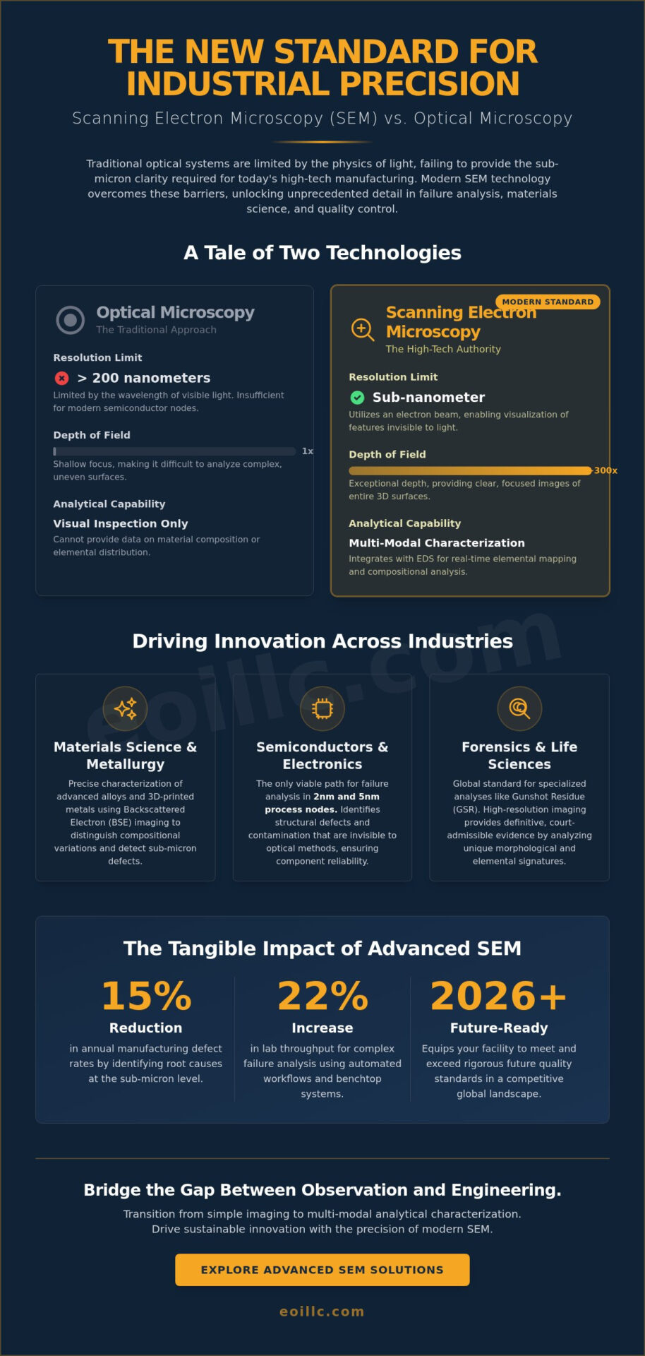
Semiconductor and Electronics: The Critical Role in Failure Analysis
The global electronics supply chain faces an existential challenge as process nodes shrink toward 2nm and 5nm architectures. At these scales, the physical limitations of light diffraction render traditional optical inspection obsolete. Light’s wavelength, typically 400 to 700nm, can’t resolve features that are now 100 times smaller. This technical barrier makes sem applications the foundational pillar of modern semiconductor fabrication. By 2026, the industry’s reliance on electron-based imaging will be absolute; it’s the only viable method to visualize the structural integrity of transistors and interconnects at the atomic scale. Without this precision, the evolutionary leap toward more efficient AI hardware and high-speed telecommunications would stall.
Identifying Micro-Defects in Integrated Circuits
IC failure analysis demands a level of scrutiny that only the Scanning Electron Microscope provides. Engineers utilize cross-sectional imaging to scrutinize the vertical architecture of interlayer dielectric layers, looking for structural anomalies. This process reveals voids or thinning that lead to catastrophic electrical leakage. When assessing wire bond and solder joint reliability, the high depth of field provided by the electron beam ensures every contact point meets rigorous industrial stress standards. Integrated Energy Dispersive X-ray Spectroscopy (EDS) adds a layer of chemical intelligence. It allows technicians to pinpoint the exact elemental composition of microscopic contaminants. Identifying a single stray atom of copper or carbon can prevent a “killer defect” from compromising a multi-million dollar production lot. A thorough understanding of the SEM working principle — including how Secondary Electrons and Backscattered Electrons are generated and detected — is essential for interpreting these signals accurately and avoiding misdiagnosis in high-stakes failure analysis.
Quality Control in Nanofabrication
Precision in the nanofabrication suite depends on Critical Dimension SEM (CD-SEM) to verify the exact widths of gate structures and trenches. Even a 0.5nm deviation can alter the switching speed of a logic gate, which impacts the overall performance of next-generation processors. Beyond inspection, the evolution of electron beam lithography (EBL) enables the rapid prototyping of complex sensor geometries that optical lithography simply can’t achieve. Maintaining high yields in a 2026 manufacturing environment requires this level of granular control. The integration of these tools into the production workflow ensures that global manufacturing standards remain high. Without the resolution offered by sem applications, the mass production of reliable high-performance computing components would be impossible.
- Resolution: SEM provides sub-nanometer resolution essential for 2nm process nodes.
- Chemical Analysis: Integrated EDS systems identify atomic contaminants that cause circuit failure.
- Structural Integrity: Cross-sectional imaging verifies the consistency of interlayer dielectric layers.
- Manufacturing Yield: CD-SEM allows for real-time adjustments to maintain high production standards.
Specialized Analytical Applications: Forensics and Life Sciences
The integration of Scanning Electron Microscopy into specialized fields has redefined the boundaries of evidentiary standards and biological research. By 2026, the precision of these instruments allows for the visualization of topographical features at the nanometer scale, a capability that is essential for both legal validation and medical innovation. The evolutionary trajectory of sem applications reflects a shift from simple observation to high-precision quantitative analysis, providing a level of reliability that matches the rigorous demands of modern global manufacturing and research sectors.
Forensic Trace Evidence Analysis
Modern criminalistics relies on SEM for more than just imaging; it’s the primary tool for Gunshot Residue (GSR) analysis. According to current forensic standards, such as those outlined in ASTM E1588-20, SEM/EDS is the global benchmark because it identifies the unique morphology and elemental composition of particles containing lead, antimony, and barium. This dual-layered verification provides a chemical fingerprint that offers a 99% confidence level in legal proceedings, far exceeding the capabilities of traditional chemical tests.
- Hit-and-Run Investigations: SEM analyzes the layered structure of paint chips and the refractive index of glass fragments to link suspects to crime scenes with high statistical certainty.
- Soil and Mineral Analysis: The system provides precise elemental maps of soil samples, allowing investigators to track a suspect’s movements based on unique mineralogical markers.
- Fiber Comparison: High-resolution imaging reveals microscopic wear patterns and dye distributions on synthetic fibers that remain invisible under optical light.
The evidentiary weight of SEM data in courtrooms stems from its ability to produce undeniable visual and chemical proof. It’s a cornerstone of forensic excellence that ensures justice is supported by technical precision rather than subjective interpretation.
Biological Morphology and Biomaterials
The synergy between high-resolution imaging and biological morphology is critical for developing next-generation medical devices. Researchers utilize sem applications to observe how bacterial colonies interact with antimicrobial surfaces at a cellular level. This analysis is vital for the success of dental and orthopedic implants. For instance, the study of osseointegration, the structural and functional connection between living bone and a load-bearing implant, requires the 10-nanometer resolution that only electron microscopy provides.
SEM enables the characterization of surface roughness on titanium alloys used in hip replacements, ensuring that the biocompatibility meets the rigorous standards of the 2026 medical landscape. This detailed surface mapping prevents implant rejection by optimizing the interface where biological tissue meets engineered materials. For a deeper look at the hardware driving these discoveries, explore Advanced SEM Techniques: A Comprehensive Guide to High-Resolution Analytical Microscopy in 2026.
To learn more about how our technical expertise can support your high-precision objectives, explore our full suite of optical and industrial solutions at EOI LLC.
Integrating Advanced SEM Applications into Laboratory Workflows
The transition from traditional, room-sized floor models to high-performance benchtop units represents a critical evolution in industrial microscopy. For decades, advanced imaging required dedicated facilities with vibration isolation and specialized cooling systems. By 2026, the decentralized model of in-house analysis has become the standard for organizations seeking to eliminate the 48 to 72-hour turnaround times common with external testing labs. Electron Optics Instruments facilitates this transition by providing the technical infrastructure necessary for immediate, high-resolution data acquisition within a compact footprint.
The Shift to High-Performance Benchtop SEMs
Modern desktop models, specifically the Cube II, now deliver 5nm resolution. This is a benchmark that previously necessitated a much larger footprint and a significantly higher capital investment. This capability allows laboratories to integrate sophisticated sem applications directly into their production lines or research bays without the need for specialized facility modifications. The Desktop SEM: The Evolutionary Shift to High-Performance Benchtop Microscopy in 2026 highlights how these systems bridge the gap between ease of use and analytical depth. Non-specialist engineers can now perform complex imaging tasks with minimal training, ensuring that precision remains a constant factor in quality control workflows.
Future-Proofing Research with Integrated EDS and Service
Sustaining the peak performance of advanced instrumentation requires a rigorous approach to maintenance and technical training. Electron Optics Instruments positions itself as a strategic partner, offering annual service contracts that guarantee analytical precision throughout the equipment’s lifecycle. These contracts aren’t just about reactive repairs; they ensure that integrated Energy Dispersive X-ray Spectroscopy (EDS) systems remain calibrated for accurate elemental analysis. This precision is vital for industries where a 1% deviation in material composition can lead to catastrophic failure.
On-site training programs further maximize the utility of specialized sem applications, empowering teams to utilize the full spectrum of features found in the Cube II and Veritas series. These instruments represent the pinnacle of modern benchtop technology, combining compact design with the power of traditional systems. By securing a comprehensive service and training partnership, laboratories ensure their research remains future-proof against the rapid technological shifts of the next decade. The synergy between high-end hardware and expert support allows for a seamless integration into existing corporate strategies.
Advancing Industrial Precision Through Evolutionary Electron Optics
The trajectory of 2026 industrial standards demands a sophisticated approach to micro-analysis where precision remains the primary metric for success. As the landscape of sem applications evolves, the integration of high-resolution imaging with quantitative data becomes indispensable for failure analysis in the semiconductor sector and advanced metallurgical characterization. These technological milestones represent a shift toward comprehensive laboratory workflows that prioritize reliability and technical excellence across global manufacturing chains.
EOI LLC leverages over 30 years of industry expertise in electron optics to facilitate these complex transitions. As the sole US distributor for EmCraft Scanning Electron Microscopes, we provide the specialized hardware required for next-generation research. Our commitment extends beyond procurement. We provide comprehensive service and preventative maintenance for all major SEM brands to ensure your operations remain uninterrupted. Precision at the nanoscale isn’t just a requirement; it’s the foundation of future innovation. We’re ready to support your pursuit of technical excellence.
Request a Consultation for Your Specific SEM Application
Frequently Asked Questions
What are the most common industrial applications for SEM?
Industrial sem applications primarily center on semiconductor fabrication, quality control in metallurgy, and polymer characterization. In 2026, the semiconductor industry relies on SEM for the inspection of 2nm gate-all-around architectures to ensure structural integrity. Automotive manufacturers utilize these systems to analyze the grain boundaries of lightweight alloys, reducing component weight by 20% while maintaining safety standards. This precision ensures global manufacturing excellence across diverse technical sectors.
Can SEM be used for elemental analysis of a sample?
SEM facilitates elemental analysis when integrated with Energy Dispersive X-ray Spectroscopy (EDS) detectors. This combination allows researchers to identify every element on the periodic table between Beryllium (4) and Uranium (92) with high precision. By detecting characteristic X-rays emitted during electron bombardment, the system generates quantitative data regarding the sample’s chemical makeup. It’s a standard requirement for 95% of material science laboratories worldwide.
How does SEM assist in failure analysis for electronics?
SEM serves as the primary tool for failure analysis in high-density electronics by identifying sub-micron defects like electromigration or solder fatigue. Technicians use it to inspect micro-vias and ball grid arrays where optical tools fail to resolve 0.1-micron fractures. Recent 2025 industry reports suggest that SEM-based inspection reduces the time required for root cause identification by 40% in complex multi-layer printed circuit boards.
What is the difference between SEM and EDS applications?
The fundamental difference lies in the data output; SEM provides high-resolution topographical imaging while EDS delivers localized chemical composition data. While SEM uses secondary electrons to visualize surface textures at 1,000,000x magnification, EDS analyzes backscattered electrons and X-rays to map elemental distribution. Most industrial sem applications require the simultaneous use of both techniques to correlate structural morphology with specific material impurities.
Is SEM applicable to biological samples in 2026?
Biological applications remain a vital frontier for SEM in 2026, specifically through the evolution of Cryo-SEM and Environmental SEM (ESEM) technologies. These methods allow for the observation of hydrated specimens, such as cellular membranes or plant tissues, without the 30% shrinkage often caused by traditional vacuum drying. Modern ESEM protocols now support the study of live microbial interactions in real-time at pressures up to 50 Torr.
Why is SEM preferred over optical microscopy for metallurgy?
Metallurgy professionals prefer SEM over optical microscopy because it offers a depth of field 300 times greater, which is essential for analyzing irregular fracture surfaces. Optical systems are limited by the physics of light to roughly 1,000x magnification and a shallow focal plane. SEM achieves 0.5nm resolution, enabling the precise measurement of crystalline structures and inclusions that dictate the mechanical performance of aerospace-grade titanium.
How has the application of benchtop SEMs changed in recent years?
Benchtop SEMs have evolved from simple screening tools into high-performance systems capable of 5nm resolution as of 2024. Their footprint has decreased by 60% compared to floor-standing models, allowing for direct integration into production lines for real-time quality assurance. This shift enables smaller firms to perform 85% of their analytical tasks in-house, bypassing the logistical delays associated with external contract laboratories.
What are the forensic applications of scanning electron microscopy?
Forensic science utilizes SEM for the definitive identification of gunshot residue (GSR) and the analysis of trace evidence like paint or fibers. Following the ASTM E1588-17 standard, investigators search for 0.5-micron particles containing lead, barium, and antimony to link a suspect to a firearm discharge. The system’s ability to provide both visual evidence and chemical confirmation makes it the gold standard in 98% of modern criminal laboratories.