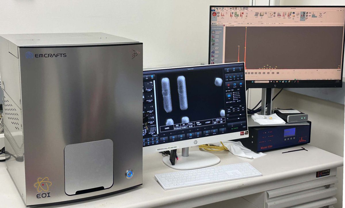
A high-resolution scanning electron microscope represents a significant capital investment, yet its analytical precision is entirely dependent on the initial 15 minutes of the workflow. You’ve likely experienced the frustration when a sophisticated instrument produces nothing but blurred, charging artifacts; a failure that accounts for approximately 65% of sub-optimal imaging outcomes in industrial laboratories. It’s a common consensus among microscopy professionals that the quality of the final micrograph is decided long before the electron beam ever strikes the surface during sem sample preparation.
By mastering these evolutionary techniques, you’ll unlock the full potential of your imaging suite and ensure superior clarity across diverse material classes. This technical guide provides a repeatable framework to eliminate charging and prevent vacuum-induced damage, allowing you to maximize the return on investment for your benchtop SEM equipment. We’ll examine the specific chemical protocols and coating advancements that are defining high-resolution standards in 2026.
Key Takeaways
- Master the evolutionary techniques of sem sample preparation to ensure structural integrity and surface cleanliness for superior high-resolution imaging.
- Distinguish the specialized methodologies required for conductive, non-conductive, and semi-conductive materials to eliminate imaging artifacts across diverse metallurgical and polymer specimens.
- Implement a standardized technical protocol that prioritizes precision cleaning and stabilization to maintain specimen rigidity under high-vacuum and electron beam environments.
- Identify and mitigate common preparation errors, such as electron charging and thermal degradation, to safeguard the accuracy of your analytical results.
- Leverage expert preparation strategies to accelerate benchtop SEM workflows while facilitating the long-term preventative maintenance of your optical systems.
The Evolutionary Role of SEM Sample Preparation in Modern Microscopy
The discipline of sem sample preparation represents the systematic engineering process required to render a specimen compatible with the rigorous high vacuum and high energy electron beam environments characteristic of modern microscopy. This protocol isn’t merely a preliminary step; it’s the definitive arbiter of image quality and analytical accuracy. In the technological landscape of 2026, where sub-nanometer resolution is a standard requirement for optical and automotive component analysis, the preparation phase serves as the critical variable in the imaging chain. It ensures three primary objectives: the establishment of surface conductivity to prevent charging, the maintenance of structural stability under thermal load, and the absolute removal of surface contaminants.
The efficacy of Energy Dispersive X-ray Spectroscopy (EDS) depends heavily on the integrity of this preparation. Poorly processed samples introduce artifacts that degrade the signal-to-noise ratio, often leading to a 15% to 20% reduction in elemental detection sensitivity. Achieving the precision necessary for advanced material characterization requires a methodical approach that aligns with the evolutionary trajectory of electron optics. Without a conductive path, electrons accumulate on the surface, creating a negative charge that deflects the primary beam and distorts the resulting data. A thorough understanding of sem operation principles and parameter tuning provides the foundational context that makes each preparation decision more deliberate and effective.
The Physics of the Vacuum Environment
Standard SEM operations occur within a high vacuum, often reaching pressures below 10^-6 Torr, to prevent electron scattering by gas molecules. Unprepared samples containing moisture or hydrocarbons pose a direct threat to the system’s integrity. Outgassing is the spontaneous release of trapped gases or volatile compounds from a material when it’s subjected to a reduced pressure environment. These released molecules can migrate through the chamber, eventually detaching and contaminating the electron optics or the objective lens. This contamination necessitates costly maintenance and results in significant system downtime for industrial laboratories. Understanding the full mechanics of how pressure is achieved and maintained is essential; a thorough knowledge of the SEM vacuum system’s theory, components, and maintenance helps technicians anticipate and prevent these contamination events before they occur.
Electron-Matter Interaction and Surface Integrity
The interaction between the primary electron beam and the specimen’s surface layers dictates the quality of the resulting data. Precision in sem sample preparation ensures that the native topography remains unaltered by mechanical or chemical stressors. Secondary electrons (SE), which originate from the top few nanometers of the surface, provide high-resolution topographical maps essential for identifying micro-fractures in automotive lighting housings or optical coatings. Backscattered electrons (BSE) emerge from deeper layers, offering contrast based on atomic number to reveal phase distributions within an alloy. Knowing exactly when to deploy each detector type is a foundational element of effective sem imaging techniques that directly complements a rigorous preparation workflow.
- Secondary Electrons: Crucial for surface morphology and edge enhancement.
- Backscattered Electrons: Essential for compositional mapping and phase identification.
- Surface Integrity: Prevents the masking of nano-scale features by oxidation or debris.
Preserving the surface integrity ensures that these electron signals reflect the true nature of the material rather than artifacts of a flawed preparation process. As we integrate more complex composite materials into global manufacturing, the ability to observe these interactions without interference becomes a cornerstone of quality assurance.
Categorizing Preparation Techniques by Material Composition
Material composition serves as the primary determinant for the specific protocols utilized in sem sample preparation. Achieving sub-nanometer resolution requires a rigorous understanding of how electrons interact with different atomic structures. Metallurgical specimens generally exhibit high electrical conductivity, which simplifies the process. Conversely, polymers and ceramics present significant hurdles due to their insulating properties. Precision in these early stages dictates the quality of the final 2026 high-resolution datasets.
Conductive vs. Non-Conductive Specimens
Metals like aluminum or steel alloys require minimal intervention. They often only need ultrasonic cleaning in an 99% isopropyl alcohol bath and secure mounting. Insulating materials such as glass or polycarbonate require a conductive bridge to prevent charging. This phenomenon occurs when the electron beam deposits a localized negative charge that deflects subsequent electrons. Technicians utilize 10-nanometer layers of gold or carbon via sputter coating to create an escape path. Grounding the sample to the aluminum stub using silver dag or carbon tape is essential for maintaining image stability. It’s the only way to ensure the electron flux doesn’t distort the topography of the specimen.
Biological and Organic Material Challenges
Organic specimens contain high water content. This is fundamentally incompatible with the 10^-6 Torr vacuum environments of modern SEM chambers. Moving from a native state to a vacuum-compatible state requires a multi-stage fixation process. Chemical fixation using 2.5% glutaraldehyde preserves the protein matrix. Following fixation, researchers employ a graded ethanol series, moving from 30% to 100%, to remove moisture. Critical point drying (CPD) using liquid carbon dioxide prevents the surface tension effects that cause structural collapse. This evolutionary approach to sample integrity ensures that delicate membranes remain intact even at 50,000x magnification.
Handling particulates involves dispersing powders onto conductive adhesive tabs to prevent individual grains from migrating under the vacuum. For moisture-sensitive materials, 2026 standards often favor cryo-SEM techniques or specialized environmental chambers. These methods maintain the sample’s hydration state through precise temperature control. Integrating these advanced optical and electronic solutions into your workflow ensures consistent data across diverse material classes. The following list outlines critical considerations for specific material types:
- Metallurgical: Focus on surface planarity and removal of oxide layers.
- Polymers: Use low voltage or conductive coatings to prevent thermal damage.
- Ceramics: Require carbon coating for energy-dispersive X-ray spectroscopy (EDS) compatibility.
- Powders: Proper dispersion is vital to avoid agglomeration and shadowing.
The transition from wet to dry states remains a technical bottleneck for many labs. Precision in sem sample preparation allows for the visualization of features that would otherwise be obscured by artifacts. By selecting the correct dehydration and coating parameters, engineers can achieve the visionary results required for modern industrial applications.

A Standardized Five-Step Protocol for SEM Sample Prep
Achieving the sub-nanometer resolution promised by 2026-era field emission microscopes demands a rigorous, repeatable approach to sem sample preparation. Any deviation from a standardized workflow introduces artifacts that obscure the true morphology of the specimen. This five-step protocol provides a technical framework for ensuring specimen integrity within the high-vacuum environment of the electron column. Of course, even the most refined preparation workflow can be undermined by an improperly configured laboratory environment; following a thorough SEM installation checklist for laboratory site preparation ensures that electromagnetic interference, vibration, and environmental factors don’t compromise the results your preparation work is designed to achieve.
- Step 1: Cleaning and Degreasing. Technicians must remove all surface hydrocarbons and oils that might outgas under the electron beam. This typically involves a 10-minute ultrasonic bath in high-purity acetone or isopropyl alcohol, followed by a nitrogen gas dry to prevent water spot formation.
- Step 2: Fixation and Stabilization. For biological or polymer-based materials, structural rigidity is paramount. Chemical fixation using 2.5% glutaraldehyde preserves the ultrastructure, while a graded ethanol dehydration series ensures the sample doesn’t collapse when the chamber pressure drops below 10^-5 Torr.
- Step 3: Mounting. The specimen is secured to an aluminum or brass stub. This stage requires the selection of a mounting medium that provides both mechanical stability and a clear conductive path to ground.
- Step 4: Coating. Non-conductive samples receive a thin, uniform layer of metal or carbon. This layer, often between 2 nm and 10 nm in thickness, prevents the accumulation of static charge which causes image “flaring” and distortion.
- Step 5: Final Inspection. Before vacuum entry, a stereomicroscope check at 40x magnification verifies that the sample is level and the conductive bridges are intact.
Advanced Mounting and Grounding Strategies
Precision in sem sample preparation extends to the selection of grounding media tailored to specific specimen geometries. Double-sided carbon tape offers a rapid solution for flat specimens, yet it may lack the mechanical stiffness required for imaging at 500,000x magnification. For complex 3D geometries or heavy metallurgical samples, silver-filled conductive paint or carbon-based epoxies are superior. These liquid media allow the technician to “paint” a conductive bridge from the top surface of the sample directly to the stub. This minimizes the resistance in the electron path. Ensuring this mechanical stability is vital; even a 2-nanometer shift during a slow-scan acquisition will result in significant motion blur.
Sputter Coating and Carbon Evaporation
Sputter coating enhances the secondary electron emission by depositing a fine grain of heavy metals like gold, platinum, or a chromium-iridium alloy. This process involves a plasma discharge that knocks atoms off a target material, which then settle onto the specimen surface. While gold coating is preferred for high-resolution topography because of its high secondary electron yield, it can interfere with chemical analysis. For projects requiring Energy Dispersive Spectroscopy (EDS), carbon evaporation is the industry standard. Carbon’s low atomic number prevents X-ray peak overlaps, which ensures that the elemental quantification remains accurate within a 0.1% margin of error.
Troubleshooting Common Artifacts and Preparation Errors
Achieving sub-nanometer resolution requires more than high-end hardware; it demands an expert understanding of how electrons interact with the specimen surface. Artifacts often manifest as subtle distortions that compromise data integrity. Charging remains the most prevalent issue, appearing as localized bright spots or sudden image shifts when electrons accumulate on non-conductive surfaces. This buildup creates an electrostatic field that deflects the primary beam, making stable imaging impossible. Beam damage is another critical concern, particularly for organic polymers or biological tissues that lack thermal stability. In these instances, the high-energy probe causes mass loss or surface melting, often visible as “bubbling” or deformation at magnifications exceeding 50,000x. Edge effects also complicate interpretation, as sharp topographical features emit a disproportionate number of secondary electrons. This leads to artificial brightness at corners that masks fine surface detail. Effective sem sample preparation protocols must account for these phenomena to ensure the resulting micrographs reflect the true morphology of the specimen.
- Charging: Identified by bright “clouds,” image streaks, or the sample physically moving.
- Beam Damage: Visible as holes, cracks, or localized melting in sensitive materials.
- Edge Effects: Excessive brightness on sharp ridges that saturates the detector.
- Contamination: Dark rectangles or spots caused by hydrocarbons polymerizing under the beam.
Mitigating Charging and Image Drift
Precision in sem sample preparation involves a strategic choice between altering the sample or the environment. If your conductive path is broken, you’ll notice erratic horizontal streaks or “drifting” where the image appears to crawl across the screen. While increasing the thickness of a gold or carbon coating can resolve this, researchers often prefer adjusting the accelerating voltage to the “charge balance point,” typically between 0.8 kV and 1.5 kV. For specimens where coating is prohibited, low-vacuum SEM modes provide a gaseous environment that neutralizes surface ions. This evolutionary approach ensures that even the most insulating materials remain stable during extended mapping sessions without the need for destructive preparation. A comprehensive checklist of sem imaging techniques for precision microscopy in 2026 can help operators systematically verify accelerating voltage, detector selection, and beam current settings to minimize these artifacts before they compromise results.
Contamination Control and Cleanliness Standards
Maintaining a pristine environment is non-negotiable for high-resolution analysis. Hydrocarbon contamination from fingerprints or residual solvents can polymerize under the electron beam, creating dark “scan squares” that obscure the sample. Lab personnel must utilize high-grade stainless steel tweezers and lint-free gloves at all times. Storage in desiccators or specialized vacuum cabinets is essential to prevent oxidation and moisture absorption. Residual moisture is a silent performance killer; it significantly degrades the Cube II Benchtop SEM vacuum performance by increasing outgassing rates. This delay in reaching high-vacuum levels can extend pump-down times by 35% or more, highlighting the need for rigorous pre-drying protocols. To ensure your lab maintains the highest standards of imaging excellence, explore our full suite of precision analytical solutions.
Optimizing Benchtop SEM Performance Through Expert Preparation
In 2026, the integration of high-performance benchtop SEMs into rapid-response industrial environments necessitates a paradigm shift in how we approach sem sample preparation. Specialized preparation techniques don’t merely improve image contrast; they accelerate the entire analytical workflow by reducing the time required for vacuum stabilization. As benchtop systems become increasingly sophisticated, the synergy between high-quality preparation and long-term preventative maintenance becomes a critical factor in maintaining operational excellence and global manufacturing standards. Precision in the early stages of the workflow ensures that the transition from sample loading to data acquisition is seamless and efficient.
Prep Quality and Vacuum System Longevity
Neglecting rigorous prep protocols often leads to catastrophic hardware degradation. Residual moisture or volatile hydrocarbons from improperly dried samples cause premature pump wear and filament failure, as these contaminants outgas within the high-vacuum chamber environment. A 2025 industry analysis indicated that approximately 40% of unscheduled service calls for benchtop units stem from sample-induced contamination. The cost-benefit analysis consistently favors rigorous preparation over frequent repairs. You can explore the financial implications of these maintenance cycles in our electron microscope cost guide, which illustrates how strategic prep investments mitigate long-term service expenses and maximize instrument uptime. It’s a matter of protecting a significant capital investment through disciplined laboratory habits. Labs that pair disciplined preparation habits with a thorough understanding of their SEM vacuum system components and maintenance requirements consistently report fewer unscheduled service interruptions and longer intervals between major overhauls.
Professional Training and Service Integration
EOI LLC provides specialized SEM training designed to standardize sem sample preparation protocols across diverse research teams. This ensures that every operator, regardless of their specific department, adheres to precision-driven standards that reflect our commitment to technical authority. Our service contracts integrate this expertise; we ensure your vacuum system stays pristine despite heavy sample loads through proactive monitoring and refined handling techniques. We develop customized protocols for specialized industrial failure analysis, focusing on the evolutionary shift toward automated preparation tools. Operators who complement these preparation skills with a mastery of advanced sem operation workflows and EDS data integration are best positioned to achieve consistent, high-throughput results across demanding industrial environments.
The transition toward automated systems represents a significant milestone in modern microscopy. By 2026, the adoption of robotic sample mounting has increased by 25% in automotive and aerospace sectors where throughput is paramount. These 2026-era tools utilize automated mounting and coating sequences to eliminate human error, ensuring that your data remains accurate and reproducible. Precision remains the cornerstone of our approach. By aligning expert training with advanced hardware service, we empower organizations to achieve repeatable, high-resolution results without compromising instrument longevity. EOI LLC remains at the forefront of this evolution, providing the technical infrastructure required to support these advanced, automated workflows. It’s about creating a sustainable ecosystem where innovation and reliability coexist.
Advancing Microscopy Standards Through Evolutionary Preparation Protocols
The path toward mastering high-resolution microscopy in 2026 hinges on the meticulous execution of sem sample preparation. By adopting a standardized five-step protocol and precisely categorizing techniques by material composition, labs eliminate the variables that lead to costly imaging artifacts. It’s clear that the intersection of expert preparation and high-performance instrumentation defines the next era of optical excellence. EOI LLC leverages over 30 years of expertise in electron optics and precision instrumentation to ensure your facility meets these rigorous standards. As the exclusive US distributor for high-performance EmCraft Benchtop SEMs, we’re positioned to support your technical evolution with specialized hardware and deep industry knowledge. Our comprehensive service contracts extend to all major SEM manufacturers, offering a total-solution approach to laboratory reliability and maintenance. Maximize your imaging precision with EOI LLC’s expert SEM training and service solutions. Your commitment to these technical refinements will undoubtedly yield superior analytical results and drive meaningful progress in your research endeavors.
Frequently Asked Questions
Why do I need to coat my SEM samples with gold or carbon?
Coating prevents surface charging by providing a conductive path for electrons to exit the specimen. Gold or carbon layers, typically 10 nanometers thick, ensure that the electron beam doesn’t build up a negative charge on non-conductive surfaces. This process increases the secondary electron yield, which improves image contrast and resolution. Without this evolutionary step in sem sample preparation, non-conductive materials like polymers or ceramics appear as bright, distorted blobs on the monitor.
Can I image wet or moist samples in a standard SEM?
You can’t image wet samples in a standard SEM because the high vacuum environment, usually maintained at 10^-5 Torr, causes rapid evaporation and structural collapse. This phase transition damages both the specimen and the microscope’s internal components. For hydrated samples, researchers must use Environmental SEM (ESEM) or cryo-SEM techniques. These specialized methods allow for pressures up to 50 Torr, preserving the sample’s natural state without the need for destructive dehydration.
How long does typical SEM sample preparation take?
Typical sem sample preparation requires between 20 minutes and 72 hours depending on the material’s complexity. A simple metallic specimen only needs 15 minutes for mounting and a 5-minute sputter coating cycle. Conversely, biological tissues require a 48-hour fixation process using glutaraldehyde followed by critical point drying. This methodical timeline ensures that the specimen’s micro-architecture remains stable under the intense energy of the 30kV electron beam.
What is the most common mistake beginners make in SEM prep?
The most frequent error is inadequate grounding of the specimen to the aluminum stub. Beginners often leave a 0.5 millimeter gap between the sample and the conductive adhesive, which leads to immediate charging. This technical oversight causes the electron beam to deflect, resulting in image drift of up to 100 microns per minute. Ensuring a continuous conductive path from the sample surface to the microscope stage is essential for capturing high-resolution data.
Is carbon tape or silver paint better for mounting samples?
Silver paint is the superior choice for high-resolution imaging and long-term stability. While carbon tape is convenient, it exhibits mechanical creep, moving up to 5 nanometers per minute under vacuum. Silver paint provides a rigid, highly conductive bond that minimizes vibration and thermal expansion. For 2026 standards of precision, silver paint’s electrical conductivity, which is 100 times greater than carbon adhesive, makes it the industry benchmark for analytical accuracy.
How does sample preparation affect EDS (Energy Dispersive Spectroscopy) results?
Sample preparation directly dictates the accuracy of Energy Dispersive Spectroscopy by introducing potential artifacts or signal attenuation. A 15 nanometer gold coating will absorb low-energy X-rays, often masking the presence of light elements like Carbon or Oxygen. Using a carbon coater instead reduces this interference. Additionally, a surface roughness exceeding 2 microns can cause X-ray shadowing, leading to a 30 percent error in quantitative elemental analysis during the detection phase.
Can I reuse SEM stubs and mounting media?
You can reuse aluminum SEM stubs after thorough cleaning, but you must discard all mounting media like tapes or resins. Reusing a stub requires a 15-minute ultrasonic bath in 99 percent pure isopropyl alcohol to remove residual adhesives and oils. Even a 1 microgram trace of old adhesive can outgas and contaminate the vacuum chamber. Because mounting media lose their chemical integrity after one vacuum cycle, they’re strictly single-use components in professional laboratories.
What happens if I put an unprepared sample into the SEM vacuum chamber?
Placing an unprepared, outgassing sample into the chamber causes a rapid vacuum failure and potential filament burnout. If a specimen contains volatile oils or moisture, the chamber pressure can spike from 10^-6 Torr to 10^-3 Torr in under 10 seconds. This sudden pressure surge triggers an emergency shutdown of the vacuum system. The resulting contamination of the final lens aperture costs approximately 4 hours of maintenance time to restore the system’s high-resolution capabilities.