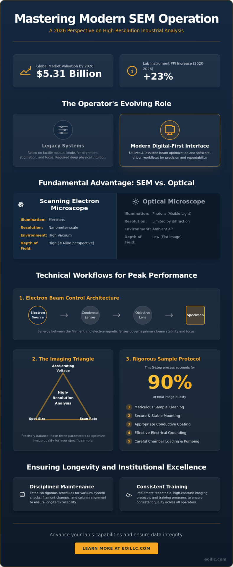
By 2026, the global scanning electron microscopy market has ascended to a valuation of 5.31 billion dollars, a figure that reflects the indispensable role of high-precision characterization in global manufacturing. This expansion places a rigorous demand on the technical proficiency of lab personnel, as the complexity of modern sem operation requires a sophisticated synergy between electron optics and vacuum physics. You recognize the persistent challenge of maintaining consistent image quality across different operators while simultaneously mitigating the risk of vacuum system contamination. It’s a delicate equilibrium where a single misaligned parameter can lead to compromised EDS data or significant hardware downtime.
Achieving the ideal balance between resolution and scan speed in high-throughput environments remains a primary concern for industry professionals who value depth and expertise. This guide provides the technical workflows necessary to master advanced parameter tuning and full EDS data integration for industrial analysis. You will gain the operational awareness required to reduce downtime and implement repeatable, high-contrast imaging protocols across your facility. Our analysis covers the evolutionary advancements in automation and the practical maintenance strategies essential for sustaining the excellence of high-end systems like the Veritas series and the Cube II Benchtop SEM.
Key Takeaways
- Understand the evolutionary transition from manual legacy controls to the digital-first interfaces of 2026 to enhance operational precision.
- Master the technical synergy between electron filaments and electromagnetic lenses to achieve superior primary beam stability and focus.
- Implement a rigorous 5-step sample mounting and grounding protocol that accounts for 90% of final image quality during sem operation.
- Optimize the Imaging Triangle by precisely balancing spot size, accelerating voltage, and scan rate for high-resolution industrial analysis.
- Establish disciplined maintenance and training schedules to ensure the long-term reliability and institutional excellence of your laboratory infrastructure.
Mastering SEM Operation: The Foundation of Modern Microscopy
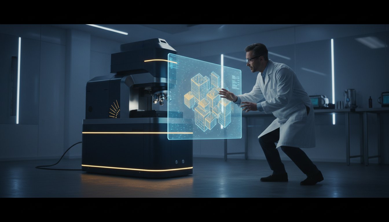
SEM operation represents the methodical governance of a high-energy electron beam within a strictly controlled vacuum environment. While legacy systems of the late 20th century relied on tactile manual knobs for alignment, the landscape of 2026 has transitioned toward a digital-first interface. This evolution, exemplified by modern systems like the Genesis Tabletop SEM, integrates sophisticated software architectures that prioritize precision and repeatability. The operator functions as a critical component of the “electron-matter interaction” feedback loop. Their decisions directly influence the signal-to-noise ratio and the veracity of the resulting data. Precision in these workflows is the primary driver of data integrity. With the Producer Price Index for laboratory analytical instruments rising 23% between 2020 and early 2026, the financial and scientific stakes of operational excellence have never been higher.
The Role of the Operator in 2026
Modern laboratory environments require a shift from manual column alignment toward AI-assisted beam optimization. In 2026, the operator’s primary responsibility involves managing the digital signal chain from the detector to the final high-resolution output. It’s no longer just about generating an image. It’s about balancing the industrial demand for high throughput with the scientific necessity for granular detail. Software-driven workflows now handle routine stigmation and focus corrections. This allows the professional to focus on interpreting complex morphological data. Ensuring that the integration of EDS results aligns with the physical topography of the specimen is now a central task. This synergy between human expertise and automated precision defines the current state of industrial characterization.
Why SEM Operation Differs from Light Microscopy
The fundamental physics of a Scanning Electron Microscope (SEM) diverge significantly from traditional optical solutions. While light microscopes are limited by the diffraction of visible light, SEM operation utilizes electrons as a high-frequency illumination source to achieve nanometer-scale resolution. This process requires a vacuum environment to prevent electron scattering by air molecules. This requirement dictates specific sample preparation protocols that are unnecessary in light microscopy. One of the most significant advantages remains the depth of field. SEM provides a 3D-like perspective that remains unattainable for optical systems. It offers a visionary look into the structural excellence of materials at the atomic level. By using electrons instead of photons, operators can bypass the physical limits of the visible spectrum to reveal the intricate details of global manufacturing components.
The Technical Architecture of Electron Beam Control
The core of high-precision sem operation resides within the column, where a complex assembly of hardware components must act in unison to generate a stable, nanometer-scale probe. This technical architecture begins at the electron source, typically a Tungsten filament or a Field Emission (FE) tip, which serves as the evolutionary starting point for the entire signal chain. While the source provides the initial electrons, the electromagnetic lenses act as the primary governors of the beam’s focal properties. Condenser lenses regulate the beam’s intensity and spot size, while the objective lens performs the final, critical convergence onto the specimen surface. This synergy ensures that the probe size remains optimized for the specific requirements of the material being analyzed, whether it’s a semiconductor wafer or a biological specimen. Scanning coils then drive the rastering process, deflecting the beam across the X and Y axes with a precision that determines the final magnification and field of view.
Managing the SEM Vacuum System
Maintaining a clean flight path for electrons is impossible without a robust vacuum system that eliminates gas molecules that would otherwise scatter the beam. Operators must navigate the transition from atmospheric pressure to high vacuum with rigorous attention to seal integrity and pump sequencing. Erratic pressure fluctuations or increased pump-down times often serve as early indicators of vacuum leaks or pump degradation. For a detailed analysis of the mechanical requirements and theory behind these systems, lab managers should consult the SEM vacuum system guide. Addressing these issues early through preventative maintenance visits is essential for protecting sensitive internal components like the Veritas HR SEM detectors from contamination.
Electron Source Optimization
Choosing between source types involves balancing resolution requirements with institutional budget realities. Tungsten filaments remained the industrial standard for conventional imaging as of 2024, holding approximately 42% of the market share due to their reliability and lower entry cost. However, Field Emission sources offer superior brightness and longevity, which are critical for high-resolution nanotechnology applications. Accelerating voltage (kV) selection is a strategic decision that directly impacts sample penetration and resolution. Lower voltages reduce sample charging and surface damage on delicate polymers, whereas higher voltages provide the deeper penetration necessary for sub-surface analysis. Proper saturation protocols are vital for extending the life of SEM filaments and consumables, as over-saturation can lead to rapid evaporation of the source material and premature hardware failure.
Strategic Sample Preparation and Loading Protocols
The success of high-precision sem operation is fundamentally predicated on the structural and electrical integrity of the specimen. Within the professional microscopy community, it’s widely accepted that approximately 90% of final image quality is determined during the preparation phase. A poorly prepared sample introduces artifacts that no amount of digital post-processing can rectify. For industrial analysis in 2026, where nanometer-scale precision is the standard, sample preparation must be treated as a rigorous engineering process rather than a preliminary chore. This methodical approach ensures that the electron beam interacts solely with the material’s true morphology, rather than surface contaminants or accumulated charge.
Achieving Conductivity and Grounding
Non-conductive specimens, such as advanced ceramics or high-performance polymers, require a deliberate grounding strategy to prevent electron build-up. When electrons accumulate on a non-conductive surface, they create a repulsive field that deflects the primary beam. This phenomenon, known as charging, often manifests as an erratic “glow” in the image or significant shifting of the field of view. To eliminate these artifacts, operators follow a 5-step mounting protocol:
- Decontamination: Remove surface oils and particulates using ultrasonic cleaning or plasma etching.
- Mounting: Secure the specimen to a specialized stub using high-purity conductive carbon tape.
- Bridging: Apply a thin line of conductive silver or carbon paint from the sample surface to the stub base.
- Sputter Coating: Deposit a conformal layer of gold, platinum, or carbon to create a uniform conductive shell.
- Verification: Perform a final mechanical inspection to ensure the sample won’t vibrate during the rastering process.
For those seeking to refine these specialized workflows, EOI LLC provides an exhaustive resource on mastering SEM sample preparation. Utilizing these techniques is essential for maintaining the data integrity required by global manufacturing standards.
Safe Loading and Chamber Evacuation
The transition from the preparation bench to the vacuum chamber represents a high-risk phase of sem operation. Operators must verify the sample height with extreme precision to prevent a physical collision with the objective lens or the EDS detector. Such an impact results in catastrophic hardware damage and significant institutional downtime. Utilizing specialized height gauges and strictly adhering to the manufacturer’s recommended working distance (WD) during the initial loading phase is a non-negotiable protocol. Cleanliness is equally paramount; the use of powder-free gloves and precision-cleaned tools prevents the introduction of hydrocarbons. These contaminants can outgas under vacuum, leading to persistent pressure fluctuations and the degradation of the vacuum system’s evolutionary performance. Monitoring the evacuation cycle for any deviation from the standard pressure curve allows for the early detection of seal failures or contaminated specimen stubs.
Advanced Parameter Tuning for High-Resolution Imaging
Mastering high-resolution sem operation requires a nuanced understanding of the “Imaging Triangle,” a conceptual framework that balances spot size, accelerating voltage, and scan rate. While a smaller spot size enhances lateral resolution, it simultaneously reduces the signal-to-noise ratio. This necessitates a slower scan rate to achieve publication-quality imagery. The operator must also select the appropriate accelerating voltage based on the specimen’s sensitivity. For instance, delicate semiconductor polymers often require low-voltage imaging below 1 kV to prevent beam-induced damage. Conversely, higher voltages are essential for maximizing the interaction volume when performing Energy Dispersive Spectroscopy (EDS). Modern 2026 interfaces, such as those found in the Veritas Pro SEM, now feature AI-driven stigmation and alignment tools. These assist the operator in correcting for astigmatism. This ensures that the electron beam remains perfectly circular, eliminating the directional blurring that once hindered manual legacy systems.
The choice between Secondary Electron (SE) and Backscattered Electron (BSE) detectors is a strategic decision dictated by the desired analytical outcome. SE detectors provide exceptional topographic detail by capturing low-energy electrons from the specimen surface. In contrast, BSE detectors reveal composition through Z-contrast. Heavier elements appear brighter due to their higher electron backscattering coefficient. Integrating these morphological insights with simultaneous EDS data allows for a comprehensive characterization of the specimen’s chemical and structural properties. This evolutionary approach to sem operation prioritizes data veracity over mere visual representation.
Optimizing the Signal-to-Noise Ratio
Optimizing the signal-to-noise ratio involves meticulous adjustment of the digital signal chain. To capture the full dynamic range of a complex sample, operators should utilize our SEM imaging techniques checklist for systematic daily calibration. Adjusting brightness and contrast ensures that no data is lost in the extreme shadows or highlights of the digital output. This precision is vital for maintaining the integrity of global manufacturing data. It’s the difference between a clear industrial insight and an ambiguous artifact.
Techniques for Industrial Failure Analysis
In industrial failure analysis, BSE mode is indispensable for identifying material density differences in cross-sections of failed automotive components. Professionals must manage complex topography in fractured surfaces while maintaining focus through precise Z-height management. These results are then documented in ISO-standardized reports to ensure compliance with global quality control frameworks. For laboratories aiming to upgrade their analytical throughput, exploring the Veritas Series SEM provides the path toward technical excellence. This integration of high-end hardware with disciplined operational protocols ensures a reliable return on investment for any research facility.
Ensuring Operational Longevity and Institutional Excellence
Disciplined sem operation serves as a strategic pillar of laboratory asset management and corporate reliability. By May 2026, the global scanning electron microscope market has reached a valuation of up to 5.31 billion dollars, a figure that underscores the immense capital invested in these analytical tools. Protecting this investment requires more than just technical skill; it demands a culture of institutional excellence where every session begins with a rigorous “operational health check.” This daily protocol verifies beam stability, vacuum integrity, and detector sensitivity before any samples are loaded. Adhering to these standards directly correlates with a reduction in annual repair costs and prevents the cascading hardware failures that often stem from minor, neglected alignment deviations.
The synergy between high-end hardware and human expertise is the primary driver of sustainable innovation in the automotive and optical sectors. While the Producer Price Index for laboratory instruments has risen 23% since 2020, organizations that prioritize operational awareness see a significant return through reduced downtime. Electron Optics Instruments, LLC positions itself as a visionary partner in this journey, providing both the precision instruments and the technical narrative required to master complex characterization. Whether you’re operating the Veritas Ultra SEM or the Cube II Benchtop SEM, your commitment to methodical workflows ensures that the data produced meets the highest standards of global manufacturing veracity.
The Value of Professional SEM Training
Transitioning to advanced platforms like the Veritas series requires a level of technical fluency that exceeds basic software familiarity. Reducing the learning curve for these sophisticated optical solutions is essential for maintaining a competitive edge in high-throughput environments. Electron Optics Instruments, LLC offers professional SEM training services designed to certify personnel in advanced parameter tuning and EDS integration. These programs allow labs to customize operational protocols for specific industry applications, ensuring that new staff members contribute to the facility’s excellence from their first day. Professional certification acts as a safeguard against the common pains of inconsistent image quality and accidental vacuum contamination.
Preventative Maintenance as an Operational Habit
Institutional longevity is built upon the habit of detailed logging and environmental vigilance. Operators facilitate the work of field service engineers by maintaining precise records of filament saturation hours and vacuum pump-down cycles. This data allows for the identification of evolutionary trends in equipment performance, enabling the scheduling of preventative maintenance visits before a critical failure occurs. Successful sem operation also depends on the stability of the laboratory environment. Professionals should regularly refer to the SEM installation checklist to monitor for changes in floor vibration or electromagnetic interference. This comprehensive approach to maintenance ensures that your laboratory remains a center of excellence, pushing the boundaries of what’s possible in modern microscopy.
Advancing Industrial Characterization through Operational Excellence
The transition toward high-precision characterization in 2026 demands a rigorous synthesis of theoretical knowledge and practical execution. Precision is non-negotiable. Mastering the nuances of sem operation requires more than a surface-level understanding of software interfaces; it necessitates a deep technical command over the electron-matter interaction and the imaging triangle. By aligning meticulous sample preparation with disciplined parameter tuning, laboratory professionals ensure the veracity of their morphological and chemical data. This structured approach to microscopy is the primary driver of institutional excellence and long-term equipment reliability in global manufacturing environments.
EOI LLC brings over 30 years of electron microscopy expertise to your facility as the sole US distributor for EmCraft SEMs. Our commitment to your success includes comprehensive on-site training and robust service contracts that safeguard your analytical throughput. We’re dedicated to providing the technical authority required to push the boundaries of what’s possible in lighting and electronics. Elevate your laboratory precision with EOI LLC SEM solutions and expert training to secure your position at the forefront of industrial innovation. Your path to technical mastery starts here.
Frequently Asked Questions
What are the most common mistakes beginners make during SEM operation?
Beginners frequently neglect to verify sample height with a physical gauge before loading. This oversight leads to objective lens collisions. Another common error involves over-saturating Tungsten filaments during the startup sequence. This practice can reduce the functional life of the source by as much as 40% according to 2024 industrial maintenance data. Proper adherence to the manufacturer’s saturation curve is essential for maintaining operational excellence.
How does accelerating voltage (kV) affect my SEM image resolution?
Higher accelerating voltages increase the depth of the interaction volume within the specimen. This provides deeper penetration but often obscures fine surface details through increased electron scattering. For high-resolution imaging of surface morphology, operators should utilize lower voltages, typically between 1 kV and 5 kV. This strategy minimizes the excitation of subsurface signals and prevents the loss of nanometer-scale topographic information.
What is the difference between SE and BSE detectors in daily use?
Secondary Electron (SE) detectors capture low-energy electrons from the surface to provide exceptional topographic detail. In contrast, Backscattered Electron (BSE) detectors respond to the atomic weight of the elements within the sample. During daily sem operation, BSE mode allows an operator to distinguish between materials of different densities. For example, a lead particle will appear significantly brighter than an aluminum substrate due to its higher backscattering coefficient.
How often should a scanning electron microscope be calibrated?
Basic operational calibrations for stigmation and focus should occur at the beginning of every imaging session. A comprehensive system-wide calibration performed by a certified field engineer is recommended every 6 to 12 months. Regular calibration ensures that the data produced remains consistent with global manufacturing standards and ISO quality control frameworks. This disciplined approach protects the integrity of long-term research projects.
Can I operate an SEM remotely in 2026?
Remote sem operation is a standard feature in 2026 for many high-throughput industrial and academic laboratories. Modern digital interfaces allow for full beam control, stage movement, and data acquisition via secure network protocols. This capability enables global engineering teams to perform real-time failure analysis and collaborative characterization without being physically present at the microscope console. It’s an evolutionary step that maximizes the utility of centralized laboratory assets.
What happens if the vacuum system fails during an active scan?
Modern systems feature safety interlocks that immediately isolate the column if the vacuum pressure exceeds a critical threshold. This protective sequence prevents atmospheric gasses from contaminating the electron source and the detector surfaces. The filament is automatically powered down to prevent oxidation and premature failure. These automated protocols are designed to minimize the risk of catastrophic hardware damage during unexpected power outages or seal failures.
How do I prevent my sample from “charging” during high-magnification imaging?
Beyond the use of sputter coating, operators can mitigate charging by increasing the scan speed and reducing the dwell time per pixel. This prevents the electron beam from lingering on a single point long enough to accumulate a significant repulsive charge. Reducing the beam current or utilizing a lower accelerating voltage also helps maintain image stability. These adjustments are vital when analyzing sensitive polymers or non-conductive ceramic components.
Is specialized training required for benchtop SEM models like the Cube II?
Yes, formal training is essential even for accessible benchtop systems like the Cube II or Genesis series. While these models feature simplified digital interfaces, improper operation can still result in vacuum leaks or expensive detector contamination. Specialized training ensures that personnel understand the technical synergy between sample preparation and hardware longevity. It’s a strategic investment that maximizes your ROI and sustains the high-tech authority of your laboratory facility.