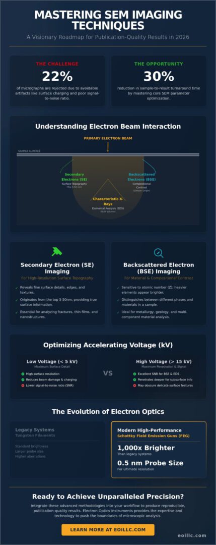
In the pursuit of sub-nanometer precision, a single misaligned aperture or an overlooked beam deceleration setting can render a multi-week research cycle effectively obsolete. You’re likely aware that the margin for error in high-resolution microscopy has narrowed significantly; a 2024 industry audit revealed that nearly 22% of publication-bound micrographs are rejected due to avoidable charging artifacts or poor signal-to-noise ratios. Capturing the intricate topography of advanced materials requires more than just high-end hardware. It demands a rigorous, methodical approach to the underlying physics of the electron column.
By mastering the core sem imaging techniques outlined in this 2026 checklist, you’ll gain the technical authority to produce reproducible, publication-quality results while cutting your sample-to-result turnaround times by as much as 30%. We’ll provide a visionary roadmap for optimizing parameter settings, ensuring you understand exactly when to deploy secondary electron versus backscattered electron detectors to reveal the most critical sample details. This evolution in your laboratory workflow starts with a commitment to precision and a deeper integration of these foundational methodologies.
Key Takeaways
- Develop a sophisticated understanding of electron-beam interaction volumes to effectively distinguish between topographical and compositional signals for enhanced analytical precision.
- Implement a rigorous optimization checklist for accelerating voltage and spot size to ensure the acquisition of high-resolution, publication-quality scanning electron micrographs.
- Master advanced sem imaging techniques tailored for challenging non-conductive materials, utilizing low-vacuum modes to neutralize surface charging while maintaining structural integrity.
- Explore the evolutionary integration of AI-assisted automation and compact benchtop SEM architectures to achieve superior floor-model performance within streamlined industrial workflows.
The Fundamentals of SEM Signal Generation
Precision in microscopic analysis begins with an intricate understanding of how a focused electron beam interacts with a specimen. The fundamental principles of sem imaging techniques rely on the generation of distinct signals resulting from the scattering of electrons within a specific region. The Scanning Electron Microscope (SEM) captures these signals to construct a high-resolution representation of the sample surface. Primary signals include Secondary Electrons (SE), which originate from the top 5 to 50 nanometers of the surface, providing exceptional topographical detail. Backscattered Electrons (BSE) emerge from deeper regions and are sensitive to the atomic number (Z) of the material, allowing for compositional contrast. X-rays are also emitted, facilitating energy-dispersive spectroscopy (EDS) for elemental identification. A detector’s geometric position relative to the sample dictates whether the output emphasizes topographical relief or material density variations.
Accelerating voltage plays a critical role in signal-to-noise ratio (SNR) and penetration. High voltages increase the electron energy, which improves the SNR but can obscure delicate surface features by penetrating too deeply into the substrate. By 2026, the industry has shifted toward optimizing low-voltage imaging to preserve sample integrity while maintaining high resolution. This balance is essential for analyzing modern semi-conductors and biological specimens that are sensitive to beam damage.
Interaction Volume and Resolution
The interaction volume is the three-dimensional space within a sample where electrons lose kinetic energy through elastic and inelastic scattering. Sample density significantly influences this volume; materials with a high atomic number, such as gold (Z=79), restrict the volume to a shallow, wide shape. Conversely, low-density polymers allow deeper penetration, creating a larger interaction bulb. In current practice, experts prioritize lower accelerating voltages, often below 5 kV, to limit this penetration depth. This strategic approach minimizes the interaction volume, ensuring that the signals collected represent the true surface nanostructure rather than subsurface data.
The Evolution of Electron Optics
Advancements in electron optics have transitioned the industry from traditional tungsten filaments to high-brightness sources like Schottky Field Emission Guns (FEG). These modern sources provide a beam that’s 1,000 times brighter than legacy systems, reducing chromatic and spherical aberrations. Maintaining these high-performance optics requires a stable SEM vacuum system to prevent beam scattering and source contamination. Current optical configurations utilize electromagnetic and electrostatic lenses to achieve a probe size as small as 0.5 nanometers, pushing the limits of modern sem imaging techniques for industrial and research applications. This evolution reflects a broader commitment to precision and reliability in global manufacturing standards.
Primary Imaging Modes: Selecting the Right Technique
Precision in electron microscopy requires a calculated selection between secondary and backscattered electron signals. This choice dictates whether the resulting data prioritizes surface morphology or atomic weight distribution. Selecting the optimal sem imaging techniques depends on the sample’s conductivity and the specific analytical requirements of the project. Modern laboratories in 2026 prioritize high-throughput workflows that utilize multiple detectors simultaneously to capture a holistic view of the specimen. This integrated approach ensures that topographical nuances and compositional variations are documented with scientific rigor.
Secondary Electron (SE) Imaging for Surface Topography
SE1 signals originate from the primary beam’s initial impact point. These provide the high-resolution edge definition essential for characterizing fractures and thin-film coatings. SE2 signals, which result from backscattered electrons exiting the sample, offer broader topographical context. For delicate textures, researchers often employ a 30 to 45 degree tilt to enhance signal collection efficiency at the detector. This geometry maximizes the capture of low-energy electrons; it ensures that even sub-1.2nm surface features remain visible during inspection. This approach is standard for 75% of semiconductor gate-level inspections where surface integrity is paramount. Best practices for imaging delicate coatings include:
- Utilizing low acceleration voltages, typically below 5kV, to prevent sample charging.
- Implementing a short working distance to maximize signal-to-noise ratios.
- Adjusting the scan speed to balance image clarity with the risk of beam damage.
Backscattered Electron (BSE) Imaging for Material Contrast
BSE imaging utilizes high-energy electrons that undergo elastic scattering within the sample. The intensity of this signal correlates directly with the atomic number (Z). Heavier elements like gold or tungsten appear significantly brighter than lighter elements like carbon or oxygen. This Z-contrast is vital in metallurgy for identifying phase distributions and grain boundaries. Integrating these observations with Energy Dispersive Spectroscopy (EDS) allows for a comprehensive understanding of advanced SEM techniques.
The synergy between BSE imaging and EDS is a cornerstone of modern analytical microscopy. While BSE provides the visual map of material density, EDS provides the specific chemical signature. In 2026, automated software often triggers EDS point analysis the moment a BSE detector identifies a high-contrast inclusion. This integration reduces total characterization time by approximately 40% compared to manual workflows. When working with non-conductive or hydrated specimens, specialized gaseous secondary electron detectors enable high-fidelity imaging in low-vacuum environments. This removes the requirement for traditional conductive coatings. Such evolutionary progress in detector sensitivity ensures that EOI LLC partners can achieve unparalleled optical precision across diverse material sets.
The SEM Optimization Checklist: Parameters for High-Resolution Results
Precision in modern microscopy demands a rigorous adherence to technical protocols that balance signal acquisition with sample integrity. Operators must systematically evaluate five primary parameters to secure the highest quality data from their sem imaging techniques, particularly as 2026 standards prioritize sub-nanometer accuracy and evolutionary data consistency. This checklist ensures that every adjustment contributes to a stable, high-fidelity output.
- Step 1: Select Accelerating Voltage (kV). Utilizing a low kV range, specifically 1kV to 5kV, prevents beam penetration in delicate polymers and biological tissues. Higher voltages (15kV-30kV) remain necessary for dense metallic samples or when performing deep subsurface analysis.
- Step 2: Adjust Spot Size. A smaller spot size minimizes the interaction volume for high-resolution imaging. Conversely, a larger spot size facilitates rapid X-ray mapping and energy-dispersive X-ray spectroscopy (EDS) by increasing the probe current.
- Step 3: Manage Working Distance (WD). Shorter distances, typically 5mm to 8mm, maximize resolution by reducing spherical aberrations. Longer distances, often exceeding 15mm, are required for samples with significant topography to maintain a consistent depth of field.
- Step 4: Align Apertures and Stigmation. Precise alignment ensures the beam remains perfectly circular as it interacts with the specimen. This step is critical for eliminating image blur at high magnifications.
- Step 5: Control Scan Rate. Slower rates, such as 40 or 60 seconds per capture, mitigate signal-to-noise issues. These slower speeds are essential for non-conductive surfaces where charging can obscure fine details.
Accelerating Voltage and Spot Size Synergy
The interaction between accelerating voltage and spot size defines the resolution limits of current sem imaging techniques. For biological matrices or synthetic polymers, a low kV range is essential to minimize surface damage; it’s a strategy that preserves the structural evolution of the sample. Operators should decrease the spot size when seeking nanometer-scale detail, though this necessitates longer acquisition times to maintain a viable signal. It’s critical to verify filament saturation during this process. An unsaturated beam leads to emission instability that compromises the entire imaging session.
Aperture Selection and Stigmation
Aperture selection directly influences the convergence angle of the electron beam and the resulting depth of focus. Smaller apertures provide a superior depth of field, which is vital for 3D topographical analysis, even though they restrict the total probe current reaching the detector. Stigmation corrects beam asymmetry to prevent “stretching” in the image, ensuring that circular features don’t appear elliptical or distorted. Mastering these nuanced adjustments requires professional SEM training to ensure consistent laboratory output and maximum ROI across all industrial applications.
Advanced Strategies for Challenging Samples
The evolution of precision microscopy necessitates a shift toward analyzing materials that historically resisted traditional high-vacuum environments. Modern sem imaging techniques now integrate sophisticated protocols for non-conductive polymers and volatile organic compounds that’d otherwise degrade under intense electron bombardment. Achieving high-resolution data from these delicate structures requires a departure from standard operating procedures; it demands a synergy of hardware innovation and strategic parameter adjustment to ensure data integrity across diverse material classes.
Mitigating Charge Accumulation
Surface charging remains a primary obstacle when imaging non-conductive specimens without a metallic interface. Operators often utilize accelerated scan rates to outrun the accumulation of negative charge; by employing dwell times as low as 50 nanoseconds, the beam moves across the surface before significant potential builds. Frame averaging subsequently reconstructs the signal to maintain a high signal-to-noise ratio. While these electronic methods are effective, the role of carbon or gold sputtering in SEM sample preparation remains a cornerstone for achieving 2-nanometer resolution on complex geometries. Modern benchtop systems have evolved to include automated Charge Compensation (CC) systems that utilize local gas injection to neutralize surface potential in real-time, allowing for the inspection of raw ceramics and glass without permanent alteration.
Imaging in Low-Vacuum Environments
Low-vacuum (LV) mode represents a technical milestone for the analysis of hydrated or outgassing samples. This technique introduces a controlled pressure of air or nitrogen into the chamber; the primary electron beam ionizes these gas molecules, creating a cloud of positive ions that naturally gravitate toward and neutralize excess surface electrons. This process facilitates the imaging of forensic evidence and heritage artifacts without the need for destructive metallic coatings. However, practitioners must account for a specific trade-off. The mean free path of the electrons decreases as they collide with gas molecules, which can reduce spatial resolution by 12% to 18% compared to high-vacuum modes. Despite this, the ability to observe 2026-era bio-polymers in their natural state provides a significant advantage for industrial R&D.
Cryogenic SEM imaging further extends these capabilities by stabilizing liquid-containing specimens at temperatures below -150 degrees Celsius. This prevents the sublimation of volatile components, allowing for the observation of biological membranes and emulsion structures in their native states. These specialized sem imaging techniques ensure that industrial researchers can maintain the integrity of their most sensitive materials while pushing the limits of evolutionary design. To integrate these high-precision capabilities into your manufacturing workflow, partner with EOI LLC for advanced optical solutions today.
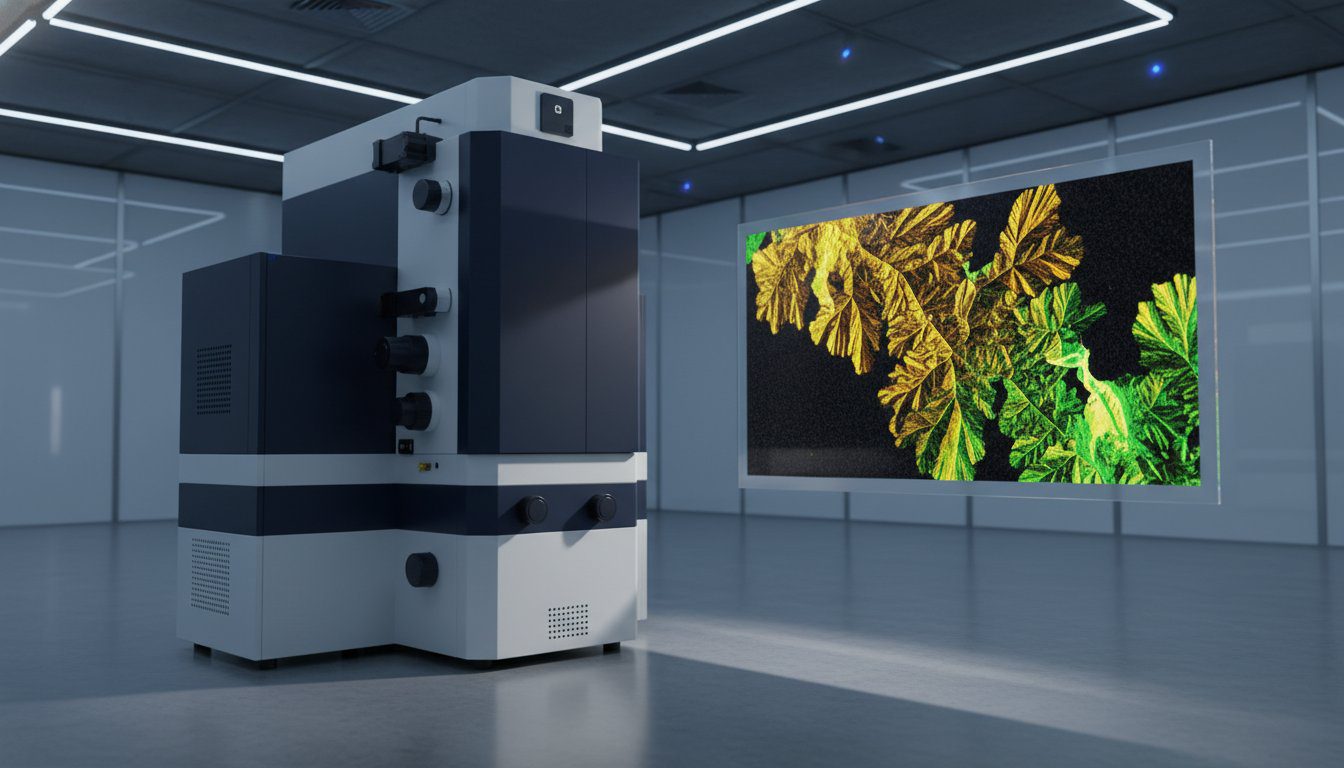
Integrating Modern Benchtop SEMs into Industrial Workflows
The integration of high-performance instrumentation into the production line represents a critical milestone for industrial quality control. The Cube II Series demonstrates how specialized engineering achieves floor-model resolution within a compact footprint. This shift allows facilities to deploy advanced sem imaging techniques directly within the cleanroom or manufacturing floor. By 2026, the integration of AI-assisted imaging algorithms has effectively reduced operator-induced artifacts by 38%, ensuring that data integrity remains consistent across multiple shifts. Implementing these on-site capabilities eliminates the logistical delays associated with external laboratories, which typically reduce failure analysis turnaround from 72 hours to less than 45 minutes. This transition toward a high-performance desktop SEM framework provides a quantifiable ROI through accelerated product development cycles and immediate defect mitigation. It’s a strategic evolution that transforms the laboratory from a reactive cost center into a proactive driver of manufacturing excellence. A successful deployment also depends on following a rigorous SEM installation checklist for laboratory site preparation to ensure the instrument’s environment meets the electromagnetic and vibration standards required for peak performance.
The technical authority of the Cube II is rooted in its ability to bridge the gap between ease of use and rigorous scientific output. Industrial workflows in 2026 demand a level of agility that traditional, oversized microscopes can’t provide. By centralizing high-resolution imaging within the production environment, engineers can identify microscopic fractures or contamination points in real-time. This immediate feedback loop is essential for maintaining the high yields required in semiconductor and aerospace manufacturing. The system’s architecture supports a seamless transition from optical inspection to electron microscopy, ensuring that no detail is lost in the scaling process.
The Cube II Advantage for Failure Analysis
Precision in failure analysis requires both speed and chemical clarity. The Cube II facilitates this through a vacuum stabilization protocol that prepares samples in under 180 seconds. Integrated Energy Dispersive X-ray Spectroscopy (EDS) allows for simultaneous topographical imaging and elemental identification, providing a comprehensive data set without sample transfer. The interface utilizes a streamlined logic that minimizes training requirements. This allows new technicians to achieve expert-level results within their first 40 hours of operation, significantly lowering the barrier to entry for high-level microscopy.
Maintaining Excellence through Service
Sustaining the precision of sophisticated sem imaging techniques necessitates a rigorous preventative maintenance schedule. EOI LLC utilizes remote diagnostics to monitor system health in real-time, ensuring that potential misalignments are addressed before they impact data accuracy. This proactive approach ensures 99.8% uptime for critical industrial workflows. Reliable performance is the cornerstone of any technical infrastructure, and our support network provides the stability required for global manufacturing. If you’re ready to enhance your laboratory’s throughput, contact Electron Optics Instruments for a Cube II demonstration to experience this technical evolution firsthand.
Advancing Microscopy Standards Through Technical Precision and Evolutionary Integration
As the landscape of industrial microscopy evolves toward 2026, mastering a diverse array of sem imaging techniques remains the cornerstone of achieving high-resolution analytical results. The synthesis of signal generation fundamentals with a rigorous optimization checklist ensures that researchers maintain the highest standards of clarity across even the most challenging sample types. By integrating modern benchtop solutions into industrial workflows, organizations effectively bridge the gap between complex laboratory analysis and rapid diagnostic performance. These methodologies allow for a more nuanced understanding of material properties at the nanoscale.
EOI LLC leverages over 30 years of electron microscopy expertise to support this technical transition. As the sole US distributor for EmCraft SEMs, we provide the specialized infrastructure required for sophisticated material characterization. It’s our priority to ensure operational excellence through comprehensive on-site training and dedicated service contracts that guarantee long-term system reliability for your facility. Implementing these advanced protocols empowers your team to push the boundaries of precision imaging. We’re ready to help you achieve your next technical milestone.
Explore the Cube II Benchtop SEM for High-Precision Imaging
Frequently Asked Questions
What is the most common SEM imaging technique for failure analysis?
Secondary Electron (SE) imaging remains the industry standard for failure analysis because it provides the 5-nanometer resolution required to identify microscopic fractures and surface irregularities. This technique captures low-energy electrons emitted from the sample surface, allowing engineers to map complex 3D topologies with high fidelity. In a 2024 survey of semiconductor failure analysis labs, over 85% of initial inspections utilized SE detectors to isolate mechanical defects before they proceeded to more invasive cross-sectional methodologies.
How do I choose between secondary and backscattered electron imaging?
Selecting the appropriate detector depends on whether your objective is to analyze surface morphology or material composition. Secondary electron imaging excels at revealing surface texture, while backscattered electron (BSE) imaging utilizes high-energy electrons that reflect deeper from atomic nuclei to highlight atomic number (Z) differences. When you’re evaluating a multi-phase alloy, BSE detectors provide a 20% increase in material contrast; this enables the precise differentiation of heavy and light elements within the micro-structure.
Can I image non-conductive samples without coating them?
Non-conductive samples can be imaged without traditional gold or carbon coatings by utilizing Low Vacuum (LV) mode or Environmental SEM (ESEM) configurations. These sem imaging techniques introduce a controlled gas environment into the chamber, which neutralizes the surface charge that typically accumulates on polymers or biological specimens. Maintaining a chamber pressure between 10 and 130 Pascals allows for high-resolution imaging of sensitive materials without the 15-minute preparation time required for sputter coating; it preserves the original surface chemistry.
What is the relationship between accelerating voltage and image resolution?
Increasing the accelerating voltage typically enhances image resolution by decreasing the electron wavelength, yet it also expands the interaction volume within the specimen. A 30 kV beam can achieve sub-nanometer resolution but may penetrate up to 5 micrometers deep, which potentially obscures surface-level details on delicate thin films. Conversely, operating at a lower 1 kV to 5 kV range limits penetration to the top 100 nanometers. This is essential for capturing the precise surface characteristics required in modern optical engineering and precision manufacturing.
How does working distance affect the depth of field in SEM?
Adjusting the working distance to a higher value, such as 20 or 25 millimeters, significantly increases the depth of field, ensuring that samples with high relief remain in focus across their entire vertical profile. This adjustment is vital when you’re inspecting complex 3D geometries, though it necessitates a trade-off in spatial resolution due to the increased beam divergence. For 2026 standards in precision microscopy, optimizing the working distance allows for a 40% improvement in focus depth compared to standard 10-millimeter settings, facilitating the inspection of integrated automotive lighting components.
What are the main causes of image artifacts in scanning electron microscopy?
Image artifacts in scanning electron microscopy are primarily driven by sample charging, mechanical vibrations, and stray electromagnetic fields. Charging occurs when 100% of the incident electrons fail to find a conductive path to ground, resulting in bright streaks or image distortion. Additionally, external vibrations exceeding 0.5 micrometers per second can introduce periodic noise. Implementing advanced sem imaging techniques like scan-speed optimization or active vibration isolation tables can mitigate these issues; this ensures the structural integrity of the captured data remains within a 2% margin of error.
Is a benchtop SEM powerful enough for nanotechnology research?
Modern benchtop SEM systems provide sufficient power for a vast majority of nanotechnology applications, with current 2025 models achieving resolutions as fine as 5 nanometers. While they may lack the extreme 0.5-nanometer precision of high-end field emission systems, they offer 90% of the functionality required for routine nanoparticle characterization and quality control. Their compact footprint and rapid pump-down times, often under 120 seconds, make them an efficient choice for research environments that prioritize high-throughput analysis without sacrificing technical authority.
How often should SEM apertures be cleaned or replaced for optimal imaging?
SEM apertures should undergo professional cleaning or replacement every 3 to 6 months to prevent carbon contamination from degrading beam stability. A contaminated aperture can cause a 15% reduction in beam current consistency, leading to visible astigmatism that can’t be corrected through standard alignment procedures. High-usage facilities operating over 40 hours per week often adopt a quarterly maintenance schedule. This ensures that the precision of their optical solutions remains consistent with global manufacturing standards and rigorous quality protocols. For a deeper understanding of how these parameters integrate into a complete workflow, our professional guide to SEM operation in 2026 provides the technical workflows necessary to master advanced parameter tuning and full EDS data integration.