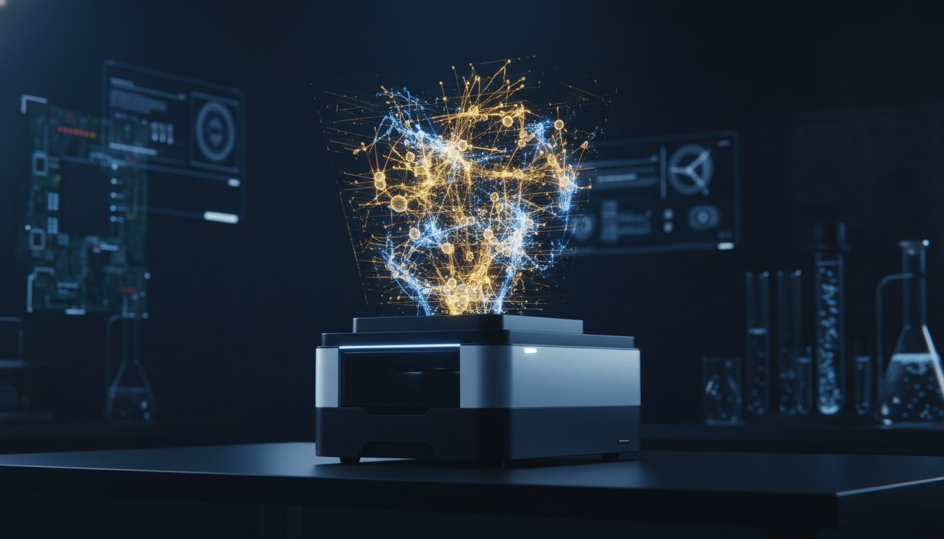
What if the requirement for a multi-million dollar centralized facility for high-resolution imaging was no longer a reality in 2026? You’ve likely navigated the frustration of sample charging obscuring critical surface details or beam intensity inadvertently melting delicate resin structures, which leads to inconclusive data and project delays. This article demonstrates how modern advancements in polymer characterization using sem now allow for the precise visualization of filler distribution and interface failure modes without the typical artifacts of traditional microscopy.
We’ll examine the technical integration of variable pressure modes and the strategic transition toward in-house benchtop systems to enhance your internal research and development capabilities. Through this expert-driven narrative, you’ll discover how to achieve superior standards in morphological analysis while maintaining the rigorous accuracy required for international industrial production. This shift represents a fundamental transformation in how industrial sectors manage quality control and failure analysis.
Key Takeaways
- Discover how sub-micron imaging enables the precise correlation between topographical data and complex material properties in modern polymer engineering.
- Identify advanced techniques to mitigate sample charging and beam-induced thermal degradation, facilitating accurate polymer characterization using sem for non-conductive specimens.
- Master the methodologies for characterizing phase morphology in immiscible blends and measuring the orientation of structural fillers like glass or carbon fibers.
- Analyze the strategic benefits of decentralizing microscopy by deploying benchtop SEM systems to accelerate quality control cycles and reduce the total cost of ownership.
- Establish a rigorous framework for selecting electron sources and automated stage configurations that align with your facility’s specific batch analysis requirements.
The Role of SEM in Modern Polymer Characterization
The requirement for precise polymer characterization using sem has evolved from a supplementary laboratory exercise into a fundamental industrial necessity. As polymer systems become increasingly sophisticated, particularly in the development of advanced thermoplastic composites, the ability to resolve features at the sub-micron level is critical for ensuring structural integrity. This transition marks a shift from simple topographical observation toward a deep correlation between material properties and structural arrangements. Modern manufacturing demands this level of scrutiny to ensure that high-performance resins meet the rigorous standards of 2026 industrial production.
Engineers now recognize that macro-scale mechanical performance is inextricably linked to microstructural morphology. By utilizing a Scanning Electron Microscope (SEM), researchers can optimize fiber-matrix interfaces and refine polymer crystallization patterns. This detailed insight allows for the reliable integration of sustainable materials into large-scale production cycles without sacrificing quality. It’s the technical authority provided by electron microscopy that empowers brands to push the boundaries of hardware innovation and technical systems.
Visualizing Surface Morphology and Topography
In medical-grade applications, the assessment of surface roughness and porosity is paramount for biocompatibility. SEM provides the meticulousness required to identify manufacturing defects, such as weld lines and sink marks, that might compromise a component’s reliability. It’s also the primary method for evaluating the efficacy of surface treatments and functional coatings. These details are often invisible to the naked eye but dictate the success or failure of a product in a clinical environment. Precise imaging ensures that every iteration of a product aligns with superior standards of accuracy.
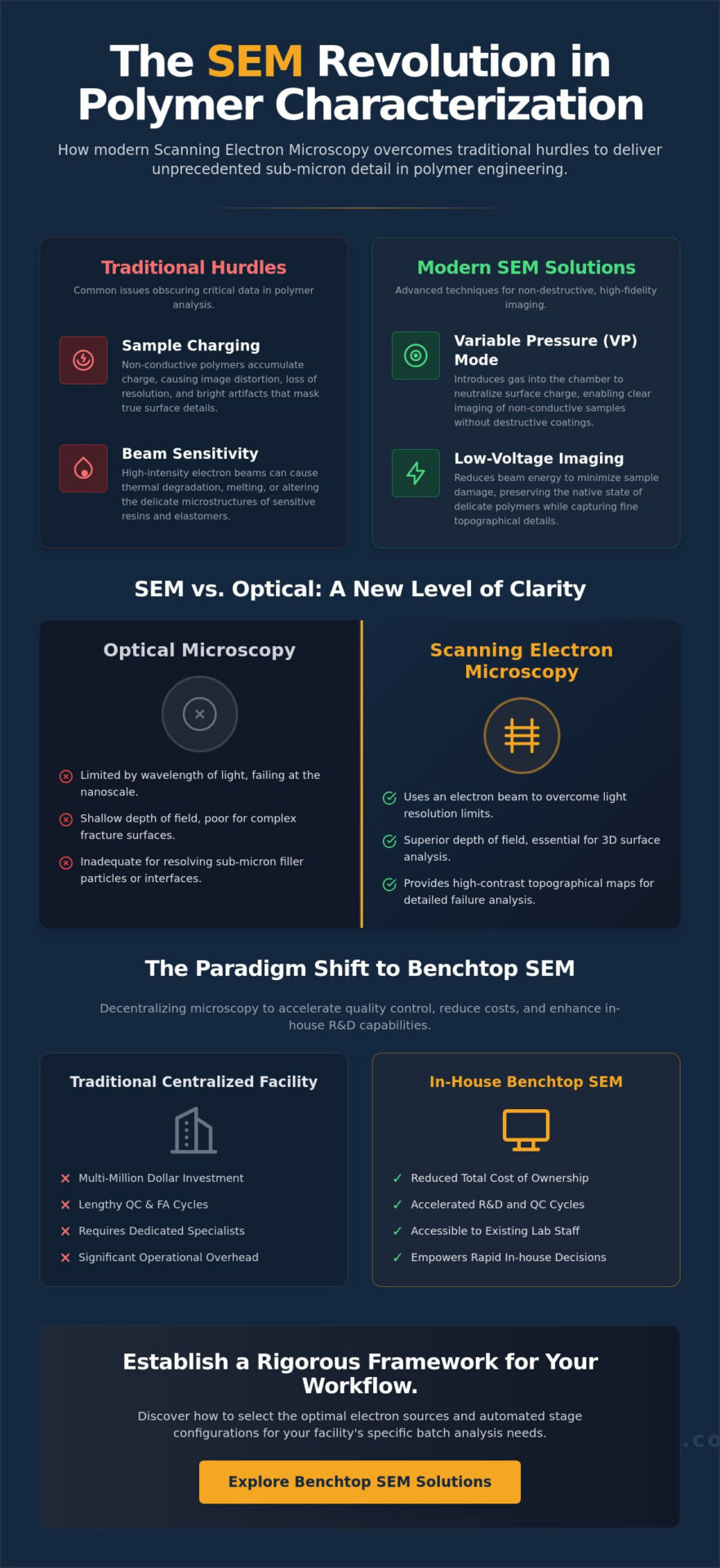
Why SEM Surpasses Optical Microscopy for Polymers
Optical systems inherently fail at the nanoscale because they’re limited by the wavelength of light. SEM overcomes these resolution limits by using an electron beam to provide a depth of field that’s indispensable for examining complex fracture surfaces. Secondary electron (SE) imaging creates high-contrast topographical maps, revealing the intricate details of a polymer’s surface. It’s a level of clarity that optical microscopes can’t match. This makes polymer characterization using sem the preferred tool for failure analysis and advanced material research, especially when dealing with the three-dimensional complexity of modern industrial polymers.
Overcoming Technical Hurdles: Charging and Beam Sensitivity
Achieving successful polymer characterization using sem requires a sophisticated understanding of the interaction between electron beams and non-conductive surfaces. Most polymers act as insulators; they accumulate negative charge when bombarded by electrons, which results in significant image distortion and loss of resolution. This phenomenon, known as the charging effect, historically forced researchers to apply conductive coatings like gold or carbon, which can mask fine surface details and alter the native state of the specimen. Modern industrial standards now favor advanced scanning electron microscopy techniques that mitigate these issues through hardware innovation rather than destructive sample preparation.
Beam sensitivity remains a secondary, yet equally critical, challenge in the analysis of delicate resins and elastomers. High acceleration voltages often lead to rapid thermal degradation, effectively melting the precise nanostructures that engineers need to examine. To preserve the integrity of these materials, the industry has shifted toward low-voltage imaging and the use of high-sensitivity detectors. These systems allow for the capture of detailed topographical data at energy levels that don’t compromise the sample’s physical properties. For facilities seeking to integrate these capabilities, exploring the latest benchtop SEM configurations can provide a reliable path toward non-destructive analysis.
Variable Pressure (VP) and Low-Vacuum Solutions
Variable pressure technology represents a paradigm shift in how we approach non-conductive materials. By introducing a controlled amount of residual gas into the chamber, the system utilizes gas molecules to neutralize surface charge through a process of ionized molecular collision. This eliminates the necessity for sputter coating, allowing for the direct imaging of wet or outgassing polymers without the risk of vacuum loss. This meticulousness ensures that the observed morphology is a true reflection of the material’s industrial performance rather than an artifact of preparation.
Optimizing Acceleration Voltage for Polymer Integrity
Finding the sweet spot between resolution and sample preservation is essential for accurate polymer characterization using sem. While traditional microscopy relied on 15kV to 30kV, modern analysis often utilizes a range between 0.5kV and 5kV to reveal authentic surface detail without inducing beam damage. The strategic use of backscattered electrons (BSE) at these lower energies provides excellent compositional contrast. This is particularly valuable when analyzing multi-phase polymer blends where identifying the distribution of different material components is vital for validating structural performance.
Analyzing Polymer Blends, Fillers, and Additives
The industrial efficacy of advanced materials depends heavily on the precise arrangement of their internal components. Whether engineering a high-impact automotive component or a sustainable packaging solution, the technical integration of fillers and additives dictates the final mechanical properties. Utilizing polymer characterization using sem allows for the meticulous mapping of phase morphology in immiscible polymer blends. This is essential for validating the performance of compatibilizers and ensuring that the discrete phases are distributed according to design specifications. Without this level of resolution, identifying the subtle boundaries between blended resins remains an exercise in speculation.
When analyzing high-performance composites, the focus shifts to the dispersion and orientation of reinforcing agents like glass or carbon fibers. Improper orientation or uneven distribution often leads to catastrophic failure under stress. By leveraging advanced SEM techniques for polymers, researchers can visualize the interface between the polymer matrix and nanoparticles with exceptional clarity. This capability is equally vital for the circular economy. Detecting metallic inclusions or foreign polymer contaminants in recycled plastic streams is necessary to maintain superior standards of quality in large-scale production and ensure logistical excellence.
Quantifying Filler Distribution and Dispersion
Achieving a uniform dispersion of fillers is a hallmark of rigorous engineering. SEM imagery provides the raw data required for the statistical analysis of particle size and spacing, which helps in identifying agglomeration issues within nanocomposites. These clusters often act as stress concentrators, undermining the material’s integrity. By observing how processing parameters, such as melt temperature or shear rate, influence filler orientation, engineers can refine their manufacturing protocols to ensure optimal structural performance and reliability across global supply chains.
Failure Analysis and Interface Characterization
The investigation of fracture surfaces, or fractography, remains a cornerstone of industrial failure analysis. High-resolution imaging allows for a clear distinction between brittle and ductile failure modes, providing clues to the underlying causes of material fatigue. In multi-layer film structures, analyzing delamination reveals weaknesses in co-extrusion processes. Similarly, investigating adhesion failure in polymer-to-metal bonds helps in optimizing chemical primers or mechanical interlocking strategies. This level of detail ensures that every industrial partner can rely on the technical authority of their characterization data to push the boundaries of what’s possible in hardware systems.
Benchtop SEM: A Paradigm Shift for Industrial Polymer Labs
The traditional model of centralized microscopy facilities often creates logistical bottlenecks that impede the pace of industrial innovation. By decentralizing these capabilities and bringing high-resolution imaging directly to the production floor, organizations can achieve a more agile response to manufacturing anomalies. The desktop SEM has undergone a significant evolutionary shift by 2026; it now offers performance levels that were previously exclusive to large-scale, floor-model systems. This transition allows for immediate polymer characterization using sem without the prohibitive infrastructure requirements or the extensive facility modifications typically associated with traditional electron optics.
Evaluating the total cost of ownership reveals that benchtop units, such as the Veritas Series or Genesis Tabletop SEM, present a more sustainable financial model for specialized industrial sectors. While traditional floor-model SEMs require dedicated rooms, vibration isolation, and constant expert oversight, modern benchtop systems operate efficiently within standard laboratory environments. The intuitive interface designs of these systems enable non-specialist personnel to perform rapid quality control checks with high repeatability. This democratization of technical authority ensures that reliability is maintained throughout the production cycle without necessitating a permanent staff of dedicated microscopists.
Speed and Accessibility in Industrial R&D
Reducing sample turnaround times from several days to mere minutes is a transformative advantage for product development teams. Rather than waiting for a centralized laboratory to process a high-volume queue, engineers can conduct real-time analysis during iterative development cycles. The compact footprint of systems like the Cube II allows for integration into space-constrained environments where traditional hardware would be impractical. This proximity to the point of production fosters a culture of meticulousness and immediate problem-solving, which is essential for maintaining a competitive edge in international production and logistical excellence.
Integrating EDS for Elemental Identification
The technical integration of EDS (Energy Dispersive Spectroscopy) Systems within a benchtop unit provides a comprehensive analytical suite for elemental identification. This is particularly valuable for the rapid detection of inorganic flame retardants, stabilizers, or cross-linking agents within a polymer matrix. By mapping elemental distribution across cross-sections, labs can ensure regulatory compliance with international standards such as RoHS and REACH. This synergy between topographical imaging and chemical analysis reinforces the stability and thoroughness required for advanced material certification. To enhance your facility’s internal characterization standards, consider exploring our complete range of benchtop SEM solutions.
Selecting the Optimal SEM for Your Polymer Workflow
Identifying the optimal hardware configuration is a strategic imperative that requires a meticulous alignment of technical specifications with specific industrial objectives. The choice of an electron source serves as the primary determinant of image quality and resolution in polymer characterization using sem. While traditional tungsten filaments offer a reliable entry point for basic topographical inspection, the superior brightness and longevity of Cerium Hexaboride (CeB6) sources, integrated into the Genesis and Cube II series, provide the enhanced contrast necessary for resolving the subtle density variations inherent in organic polymers. For organizations pushing the boundaries of nanotechnology, the Veritas FE SEM provides the ultimate field-emission stability required to characterize features at the extreme nanoscale with unwavering accuracy.
Beyond the electron source, the integration of automated stage movement is essential for modern high-throughput environments. This capability facilitates consistent batch analysis, allowing for the characterization of multiple specimens without the variability introduced by manual positioning. To maintain these superior standards of precision, professional SEM maintenance is a non-negotiable requirement for operational uptime. Electron Optics Instruments supports the national polymer industry by providing the technical authority and hardware reliability necessary to transition complex research into scalable industrial performance. This partnership ensures that your laboratory remains at the intersection of innovation and logistical excellence.
The Cube II and Genesis Series Advantage
The Cube II and Genesis series are engineered to provide high-brightness CeB6 illumination, which is particularly effective for imaging non-conductive polymer surfaces with minimal beam damage. These systems feature user-friendly interfaces designed specifically for material scientists who require rapid data acquisition without the steep learning curve of traditional electron optics. Their inherent versatility allows for the handling of diverse sample sizes, from thin films to complex molded components, ensuring that every phase of the development cycle is supported by high-resolution morphological data.
Professional Training and Service Implementation
Successful implementation of advanced microscopy requires more than just high-end hardware; it necessitates a comprehensive support structure. We provide customized on-site training that focuses on polymer-specific imaging protocols, ensuring your team can maximize the potential of their polymer characterization using sem. Equipment longevity is further secured through our scheduled preventative maintenance visits and the ready availability of SEM filaments and consumables. This steady, expert-driven narrative of support provides direct access to technical specialists, empowering your facility to overcome complex characterization challenges while maintaining the rigorous standards of 2026 industrial production.
Advancing Industrial Standards through Precision Microscopy
The landscape of material science in 2026 demands a rigorous approach to structural analysis; one that prioritizes both resolution and operational efficiency. By implementing the advanced imaging strategies discussed, such as low-voltage optimization and variable pressure modes, laboratories can achieve definitive results in polymer characterization using sem without compromising sample integrity. This evolution from centralized, high-maintenance infrastructure toward agile, benchtop-driven workflows ensures that high-performance polymer blends and composites meet the exacting requirements of global production cycles.
As the sole US distributor for EmCraft SEMs, Electron Optics Instruments leverages over 30 years of specialized expertise in electron optics to provide reliable technical integration for your facility. We offer comprehensive on-site training and national service support to ensure your hardware maintains superior standards of accuracy over its entire lifecycle. Explore the Cube II Benchtop SEM for your polymer laboratory to discover how meticulous hardware design can transform your internal R&D capabilities. We look forward to supporting your organization’s journey toward technical excellence and industrial growth.
Frequently Asked Questions
Do all polymer samples require a conductive coating for SEM analysis?
No, the requirement for conductive coating is no longer universal due to the integration of variable pressure (VP) and low-vacuum modes in modern hardware. These systems utilize residual gas molecules to neutralize surface charge; this allows for the direct imaging of non-conductive specimens in their native state. This approach is essential for preserving the authentic morphology of delicate resins that might otherwise be obscured by sputter-deposited gold or carbon layers.
How do I prevent my polymer sample from melting under the electron beam?
Minimizing thermal degradation requires a reduction in acceleration voltage, typically within the range of 0.5kV to 5kV. By utilizing lower beam currents and faster scanning speeds, you can effectively manage the energy dose delivered to the specimen. Modern benchtop systems also feature high-sensitivity detectors that capture high-resolution data at these reduced energy levels, ensuring the structural integrity of the polymer isn’t compromised during the imaging process.
What is the difference between SE and BSE imaging for polymer blends?
Secondary Electron (SE) imaging is primarily utilized to visualize surface topography and fine morphological details. In contrast, Backscattered Electron (BSE) imaging provides compositional contrast based on atomic number differences. This is particularly valuable for polymer characterization using sem when analyzing multi-phase blends or composites, as it allows for the clear differentiation between the polymer matrix and inorganic fillers or additives.
Can a benchtop SEM achieve the resolution needed for nanoparticles in polymers?
Yes, modern benchtop systems equipped with high-brightness Cerium Hexaboride (CeB6) or Field Emission (FE) sources can resolve nanoparticles within a polymer matrix. For instance, the Veritas FE series provides the high-resolution capabilities necessary to identify nanoparticle dispersion and agglomeration. These advancements ensure that benchtop hardware remains a viable solution for the rigorous standards of 2026 industrial research and development.
How does integrated EDS help in polymer failure analysis?
Integrated Energy Dispersive Spectroscopy (EDS) systems allow for the simultaneous acquisition of chemical data alongside topographical images. This synergy is critical for identifying foreign contaminants, assessing the distribution of flame retardants, or analyzing the chemical nature of inclusions at a fracture site. By correlating elemental mapping with morphological defects, engineers can pinpoint the precise root causes of material failure in complex polymer systems.
What are the environmental requirements for installing a benchtop SEM?
Benchtop SEMs are designed for installation in standard laboratory environments without the need for specialized infrastructure. They require a stable, level bench and a standard power outlet. While they’re more robust than floor models, minimizing proximity to heavy machinery or significant electromagnetic interference will ensure the highest image quality. This small footprint and lack of complex facility modifications facilitate rapid deployment across diverse industrial settings.
Is it possible to image liquid or hydrogel polymers with an SEM?
Imaging liquid-phase or hydrogel polymers is achievable through the use of variable pressure (VP) or environmental SEM modes. These configurations allow for the maintenance of a higher pressure within the sample chamber, which slows the evaporation of volatile components. This capability is essential for characterizing the porous structures of hydrogels or observing the interaction of polymers in a semi-hydrated state without the collapse of delicate microstructures.
How often does a benchtop SEM require maintenance in a high-volume polymer lab?
In high-volume industrial environments, we recommend scheduled preventative maintenance visits at least once or twice per year to ensure optimal performance. The frequency of filament replacement depends on the source type; tungsten filaments require more frequent changes compared to the long-life CeB6 sources found in the Genesis and Cube II series. Maintaining a consistent supply of SEM filaments and consumables is vital for ensuring continuous uptime in rigorous polymer characterization using sem workflows.