

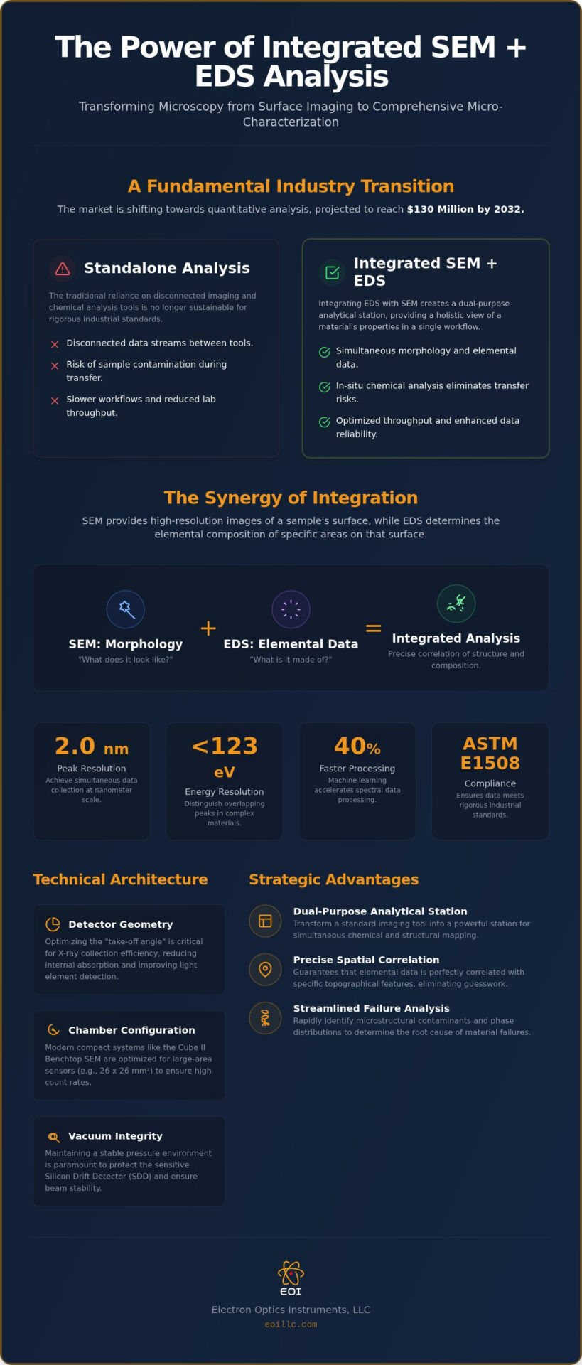
The global EDS detectors market is projected to reach USD 130 million by 2032, a trajectory that underscores a fundamental industry transition from qualitative surface imaging toward comprehensive, quantitative micro-characterization. Most practitioners recognize that the traditional reliance on disconnected data streams between separate imaging and chemical analysis tools is no longer sustainable for rigorous industrial standards. By integrating eds with sem, organizations can transform their microscopy workflows to achieve simultaneous morphology and elemental data collection at resolutions as fine as 2.0 nanometers, ensuring compliance with established specifications such as ASTM E1508.
This technical guide explores how the latest 2026 hardware advancements, such as the Bruker XFlash FlatQUAD 2L and the Veritas HR SEM series, streamline failure analysis and quality control processes. We’ll examine the specific hardware requirements for benchtop SEM integration and the role of machine learning in accelerating spectral processing by up to 40 percent to ensure your laboratory maintains its competitive technical authority and operational excellence in an increasingly demanding global market.
Key Takeaways
- Understand how integrating eds with sem transforms a standard imaging tool into a dual-purpose analytical station for simultaneous chemical and structural mapping.
- Identify the critical hardware parameters, such as detector geometry and optimal take-off angles, that are essential for ensuring precise X-ray collection within the SEM chamber.
- Learn the implementation best practices for managing accelerating voltage and beam current to maintain a balance between high-resolution morphology and reliable elemental signal detection.
- Recognize the strategic advantages of integrated workflows for failure analysis, specifically in streamlining the identification of microstructural contaminants and phase distributions.
- Explore how specialized platforms such as the Cube II Benchtop SEM and Veritas Series provide the necessary stability and sensitivity for advanced elemental characterization.
The Synergy of Integrating EDS with SEM for Material Characterization
The evolution of industrial microscopy has necessitated a definitive shift from isolated observation toward a unified analytical paradigm. By integrating eds with sem, researchers move beyond mere morphological inspection to achieve a state of comprehensive elemental characterization within a single operational environment. This synergy is indispensable for contemporary industrial failure analysis, where the ability to correlate microstructural anomalies with chemical signatures determines the efficacy of quality control protocols. Modern Silicon Drift Detectors (SDDs) facilitate this by providing the high-speed data acquisition required to maintain pace with advanced electron optics, ensuring that precision and reliability remain the benchmarks of every investigation.
What is Energy Dispersive Spectroscopy (EDS)?
Energy-dispersive X-ray spectroscopy (EDS) functions through the detection of characteristic X-rays generated during electron beam interaction with the sample’s atomic structure. As the primary beam displaces inner-shell electrons, the subsequent relaxation of outer-shell electrons into these vacancies emits X-ray photons with discrete energy values. The detector quantifies these energies to determine the specific elements present. Maintaining superior spectral resolution is critical for the accurate identification of atomic species, particularly when distinguishing between overlapping peaks in sophisticated semiconductor or metallurgical samples. Current SDD technology allows for energy resolutions below 123 eV, providing the meticulousness required for complex material systems.
The Advantage of In-Situ Chemical Analysis
The methodology of integrating eds with sem ensures that the chemical data remains perfectly correlated with the specific topographical features observed during imaging. Performing chemical analysis in-situ eliminates the logistical risks and data inaccuracies associated with sample transfer between separate imaging and spectroscopic instruments. It’s a streamlined approach that guarantees a precise spatial correlation between surface topography and elemental distribution, providing a holistic view of the material’s properties. This integration significantly optimizes laboratory throughput and enhances the technical authority of the analytical process. For those utilizing the Cube II Benchtop SEM or platforms within the Veritas Series, this capability translates into a more robust understanding of material performance and failure mechanisms through immediate, high-fidelity data collection.
Technical Architecture of Integrated Analytical Systems
The structural architecture of a high-performance analytical system requires meticulous spatial coordination within the vacuum chamber. When integrating eds with sem, engineers must account for the volumetric displacement of the detector while preserving the vacuum integrity essential for secondary electron imaging. Maintaining a stable pressure environment is paramount. Any fluctuation can compromise the electron beam’s mean free path or contaminate the sensitive Silicon Drift Detector (SDD) window. Modern systems like the Veritas HR SEM are engineered to accommodate these analytical additions without sacrificing their 2.0 nanometer peak resolution, ensuring that structural and chemical data remain equally sharp and reliable.
Detector Geometry and Chamber Configuration
Optimizing the “take-off angle” is the most critical factor for X-ray collection efficiency. This angle, formed between the sample surface and the detector’s centerline, dictates the path length X-rays must travel through the sample material before reaching the sensor. A shorter path reduces internal absorption, which is vital for the accurate detection of light elements. To maximize signal-to-noise ratios, the working distance must be precisely calibrated to align the sample’s focal point with the detector’s line-of-sight. In compact systems like the Cube II Benchtop SEM, chamber configuration is optimized to allow for large-area sensors, such as the 26 x 26 mm² active area found in 2026-spec detectors, ensuring high count rates even at lower beam currents.
Software Synchronization and Data Fusion
Effective integration extends into the digital layer, where software suites like Bruker Quantax Studio or Oxford Instruments AZtecLive facilitate the fusion of morphological and chemical data. Practitioners can now map elemental distributions directly onto high-resolution backscattered electron (BSE) images in real time. This “spectral imaging” approach collects a full energy spectrum at every pixel, allowing for retrospective analysis without re-scanning the sample. By 2026, automated peak identification and deconvolution algorithms have become standard. These systems utilize machine learning to resolve complex overlaps between elements, such as the proximity of Molybdenum L-alpha and Sulfur K-alpha lines. This level of algorithmic precision ensures that the resulting chemical maps are both accurate and reproducible across different operators. If you’re looking to upgrade your laboratory’s capabilities, exploring integrated EDS solutions can provide the necessary technical edge to master these complex workflows.
Strategic Benefits: Why Integrated Systems Outperform Standalone Analysis
Standalone analysis often involves a disjointed sequence of events that introduces variables and potential data misalignment. By integrating eds with sem, laboratories establish a cohesive analytical environment where morphological and chemical data are captured under identical vacuum conditions. This consolidation is not merely a convenience; it’s a strategic upgrade that enhances the fidelity of phase distribution analysis and the identification of sub-micron contaminants. It ensures that the researcher remains focused on the sample’s properties rather than the logistics of data correlation.
Integrated systems allow for the immediate correlation of grey-level contrast in BSE images with specific atomic numbers. This prevents the frequent misinterpretation of structural artifacts as chemical inclusions. Additionally, the cost-effectiveness of benchtop SEMs with integrated EDS has made high-end characterization accessible to industrial labs that previously relied on standalone spectrometers. Consolidated reporting ensures that all metadata, including accelerating voltage and working distance, is preserved within a single data file, which is essential for maintaining rigorous standards in international production and logistical excellence.
Real-Time Elemental Mapping and Line Scans
Modern Silicon Drift Detectors (SDDs) have achieved count rates exceeding 100,000 counts per second, which radically accelerates the generation of high-resolution elemental maps. These maps enable the visualization of subtle chemical gradients across grain boundaries or complex multi-layer coatings that are often invisible in standard imaging. Line scans provide a quantitative profile of diffusion layers in metallurgical samples, allowing engineers to measure the depth of heat-treatment effects or oxidation with surgical precision. This level of detail is vital for industries focused on advanced hardware and technical systems where material purity is non-negotiable.
Enhanced Throughput in Industrial Failure Analysis
Transitioning to an integrated benchtop platform like the Cube II SEM reduces the reliance on external laboratory services, which often introduce delays into the production cycle. In manufacturing, the rapid identification of foreign object debris (FOD) is critical for maintaining operational stability. Automated elemental checks on semiconductor wafers ensure that deviations in composition are detected before they lead to large-scale production failures. This in-house capability transforms failure analysis from a reactive necessity into a proactive tool for sustainable industrial performance. It allows for a steady, deliberate flow of information that matches the rigorous internal processes of global innovators.
Implementation Best Practices for Integrated EDS-SEM Workflows
The successful execution of an analytical protocol depends on the operator’s ability to synchronize electron beam physics with the detector’s collection requirements. When integrating eds with sem, achieving high-fidelity results is a matter of balancing conflicting hardware demands. High-resolution imaging typically favors low accelerating voltages and small spot sizes to minimize the interaction volume; yet, quantitative chemical analysis often requires higher energy to excite characteristic X-rays. Maintaining this equilibrium ensures that the data collected is not only visually sharp but also chemically accurate, reflecting the meticulous standards required in specialized industrial sectors.
Optimizing Beam Parameters for Dual-Signal Collection
Adhering to the ‘Overvoltage’ rule is paramount for reliable element identification. The primary electron beam energy should ideally be 1.5 to 2 times the energy of the highest X-ray line of interest to ensure efficient ionization. While increasing the beam current enhances the X-ray count rate and improves the signal-to-noise ratio, it simultaneously increases the beam’s spot size, which can degrade the clarity of secondary electron images. The size of the interaction volume, which expands with increasing accelerating voltage, fundamentally limits the spatial resolution of the resulting elemental data regardless of the electron beam’s diameter.
Sample Preparation for Accurate Elemental Data
Topographical features can significantly skew elemental results by introducing shadowing effects or altering the X-ray path to the detector. For quantitative analysis, samples must be prepared with a flat, polished surface to ensure a consistent take-off angle across the entire area of interest. Selection of conductive coatings is equally critical. Carbon is the preferred medium for EDS as its characteristic K-alpha peak rarely interferes with heavier elements. Gold coatings, while superior for imaging, can mask critical peaks in the 2.1 keV range, such as Molybdenum or Sulfur. Proper sample tilt must also be managed to maintain a direct line-of-sight between the specimen and the sensor window, ensuring that the detector captures a representative signal from the interaction site.
The technical synergy between hardware stability and analytical precision is a cornerstone of reliable data. Regular calibration against known standards is essential to account for detector drift and maintain energy resolution below 123 eV. Neglecting preventative maintenance visits can lead to a gradual loss of sensitivity or vacuum-induced contamination of the detector window, compromising the integrity of longitudinal studies. Professional training and rigorous maintenance schedules act as the anchors for consistent, high-end production standards in any advanced industrial facility, ensuring that your integrated system remains a visionary tool for innovation and reliability.
Advanced Integrated Solutions from Electron Optics Instruments
Achieving technical excellence in 2026 requires more than just high-specification hardware; it demands a synergy between advanced instrumentation and expert-led operational support. Electron Optics Instruments has established itself as a seasoned, global innovator by providing platforms specifically engineered for integrating eds with sem. Whether your facility focuses on high-throughput quality control or specialized metallurgical research, our systems are configured to deliver the meticulous accuracy and reliability that modern industry professionals demand. Our role as the sole US distributor for EmCraft Scanning Electron Microscopes ensures that our clients receive direct access to cutting-edge technology backed by over 30 years of industry experience.
The Cube II: Redefining Benchtop Analytical Microscopy
The Cube II Benchtop SEM represents a transformative shift in localized material characterization. This platform is designed to house sophisticated EDS detectors within a compact footprint, maintaining the stability required for high-resolution imaging and simultaneous elemental mapping. Its user-friendly interface bridges the gap between novice operators and seasoned researchers, allowing for rapid deployment in industrial environments. By providing a stable vacuum and optimized detector geometry, the Cube II ensures that your team can transition seamlessly from morphological observation to quantitative chemical analysis without the logistical delays of larger, floor-standing units.
Beyond the benchtop, our Veritas Series SEM offers a modular architecture that can be customized for highly specialized analytical research. These systems provide the peak resolution and beam stability necessary for characterizing advanced materials and semiconductor components at the nanometer scale. They act as recurring anchors for labs that prioritize superior standards in their developmental outlook.
Expert Support for Long-Term Analytical Precision
The longevity of an integrated analytical system is fundamentally tied to the rigor of its upkeep. Consistent SEM maintenance is essential for preserving the sensitivity of the Silicon Drift Detector and preventing vacuum-related degradation of the electron source. Our national service network provides tailored maintenance contracts that cover both the SEM hardware and the integrated EDS components; this ensures that your instrument remains compliant with international standards like ASTM E1508. We prioritize meticulousness in every service visit to maintain the high-end quality your operations require.
To complement our hardware, we offer comprehensive on-site technical training. This expert-led instruction empowers your team to master the complexities of integrating eds with sem, from peak deconvolution to automated mapping protocols. By combining our reliable hardware with a steady, deliberate flow of technical expertise, we ensure that your laboratory’s internal processes are as rigorous as the systems you operate. This holistic approach reinforces our status as a high-tech authority and a reliable partner in your pursuit of industrial excellence.
Advancing Analytical Standards through Integrated Microscopy
The successful transition from purely morphological observation to comprehensive micro-characterization depends on the technical synergy between electron optics and spectroscopic detection. By integrating eds with sem, organizations move beyond fragmented data collection to achieve a unified analytical workflow that mirrors the rigorous standards of international production. This process requires a meticulous approach to hardware configuration; optimizing detector geometry and beam parameters ensures the fidelity of every spectrum captured. Whether utilizing the high-performance Cube II Benchtop SEM or the specialized Veritas Series, the goal remains a stable, visionary platform for innovation.
Electron Optics Instruments brings over 30 years of industry expertise to your facility as the sole US distributor for EmCraft systems. Our commitment to reliability is reflected in our national on-site service and comprehensive technical training programs, which are designed to maximize your team’s proficiency. We invite you to request a technical consultation for your integrated SEM-EDS needs to ensure your laboratory maintains its status as a high-tech authority. It’s time to transform your imaging capabilities into a powerful, multi-dimensional tool for structural and chemical excellence.
Frequently Asked Questions
What is the primary benefit of integrating EDS with an SEM?
The primary benefit is the immediate correlation of high-resolution surface morphology with discrete chemical composition during a single analytical session. By integrating eds with sem, researchers eliminate the data misalignment risks inherent in utilizing separate analytical tools. This unified approach facilitates the rapid identification of sub-micron contaminants and phase distributions, which is critical for maintaining logistical excellence in high-end industrial production environments.
Can any SEM be retrofitted with an EDS detector?
Retrofitting is possible only if the SEM chamber contains an appropriately angled port with a direct line-of-sight to the sample’s focal point. While many floor-standing units are designed for expansion, benchtop systems often require factory-integrated configurations to preserve vacuum integrity and detector geometry. It’s essential to verify that the chamber’s volumetric capacity can accommodate the detector’s cooling and electronics without compromising electron beam stability.
Does integrating EDS affect the imaging resolution of the SEM?
Integrating an EDS detector doesn’t inherently degrade the SEM’s imaging resolution, as the hardware remains physically separate from the primary electron column. However, operators must maintain precise column alignment and ensure the detector’s cooling system doesn’t introduce mechanical vibrations. Modern platforms like the Cube II are engineered to preserve their peak resolution while simultaneously capturing high-count-rate X-ray signals for comprehensive characterization.
What is the difference between qualitative and quantitative EDS analysis?
Qualitative analysis focuses on identifying which elements are present by matching spectral peaks to characteristic energy levels. Quantitative analysis goes further by calculating the mass or atomic percentage of each element, often requiring comparison against known standards or the use of sophisticated ZAF correction algorithms. Achieving quantitative accuracy requires a flat, polished sample surface to ensure a consistent X-ray take-off angle to the detector sensor.
How much training is required to operate an integrated EDS-SEM system?
Basic operation for qualitative mapping can often be mastered within a few days of technical training; however, achieving proficiency in quantitative deconvolution requires a deeper understanding of electron physics. Electron Optics Instruments provides on-site technical training to help teams navigate these complex analytical protocols. Mastery of the software’s advanced peak identification features is essential for ensuring the reliability and meticulousness of your laboratory’s output.
What accelerating voltage is typically needed for EDS analysis?
Selecting the correct accelerating voltage is governed by the ‘Overvoltage’ rule, which suggests using a beam energy 1.5 to 2 times higher than the energy of the highest characteristic X-ray line being analyzed. For metallurgical samples containing heavier elements, 15 to 20 kV is standard; conversely, light element analysis may utilize lower voltages to minimize the interaction volume. Proper voltage selection is a cornerstone of the process when integrating eds with sem.
How often does an integrated EDS system require calibration?
Integrated EDS systems require regular energy calibration to account for electronic drift and maintain a spectral resolution below 123 eV. While automated software checks can be performed daily, a formal calibration against a standard material, such as copper or cobalt, should be conducted monthly. Adhering to a schedule of preventative maintenance visits ensures that the detector’s window remains free of contamination, preserving long-term analytical precision and reliability.
What are the limitations of EDS when integrated with a benchtop SEM?
The primary limitations include a detection threshold of approximately 0.1 weight percent and occasional difficulty resolving elements with closely overlapping spectral peaks. Additionally, compact benchtop systems may have smaller detector active areas compared to large-scale research instruments, which can result in lower count rates for certain trace elements. Despite these factors, the efficiency of a benchtop integrated system remains superior for high-throughput failure analysis and routine quality control.