
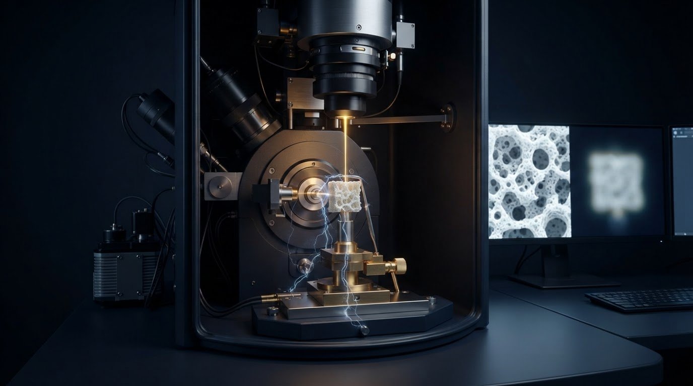
The pursuit of sub-nanometer resolution often founders not on the inherent limitations of the electron column, but on the volatile accumulation of surface electrons that renders non-conductive materials nearly impossible to visualize without significant distortion. You’ve likely encountered the persistent frustration of image blooming and localized heating, where the very energy intended to reveal a sample’s morphology instead destroys its integrity or obscures accurate EDS analysis. This guide serves as a comprehensive technical framework for mastering the protocols required for high-resolution imaging while avoiding charging on insulating samples. By strategically balancing landing energies with variable pressure environments, researchers can achieve crisp, high-contrast results without the traditional reliance on heavy conductive coatings.
We’ll examine the critical synergy between low-voltage imaging and modern instrumental capabilities, such as those found in the Cube II and Veritas HR SEM systems, to provide you with the expertise needed to navigate the complexities of non-conductive material characterization. Through precise adjustments to vacuum levels and the exploitation of advanced field emission sources, it’s now possible to maintain charge stability for most industrial polymers while ensuring superior standards in analytical accuracy. This methodical approach ensures your laboratory achieves meticulous results while significantly reducing total sample preparation time.
Key Takeaways
- Gain a comprehensive understanding of the electron dynamics that drive surface instability to establish more effective protocols for avoiding charging on insulating samples.
- Learn to identify the optimal balance between sputter coating and native-state imaging while utilizing conductive mounting methods to facilitate proper grounding.
- Implement precise instrumental adjustments, including the reduction of beam current and the adoption of low-voltage strategies, to mitigate localized thermal damage.
- Discover scanning strategies that utilize Backscattered Electron (BSE) detectors and reduced dwell times to capture high-contrast, artifact-free topographical data.
- Explore how the integrated automation of the Cube II and Genesis systems simplifies the characterization of challenging insulators through sophisticated vacuum management.
Understanding the Physics of Sample Charging in Scanning Electron Microscopy
Electrostatic charging represents a fundamental challenge in electron optics, occurring when the incident primary electron beam deposits a higher density of electrons than the specimen can effectively dissipate. In a standard Scanning electron microscope, this instability arises because non-conductive materials lack the mobile charge carriers necessary to facilitate a consistent path to ground. When the electron inflow exceeds the total outflow, the resulting surface potential creates a localized electric field that deflects the primary beam, leading to significant image distortion. Mastering the underlying physics of this interaction is the first prerequisite for avoiding charging on insulating samples.
The Mechanism of Electron Accumulation
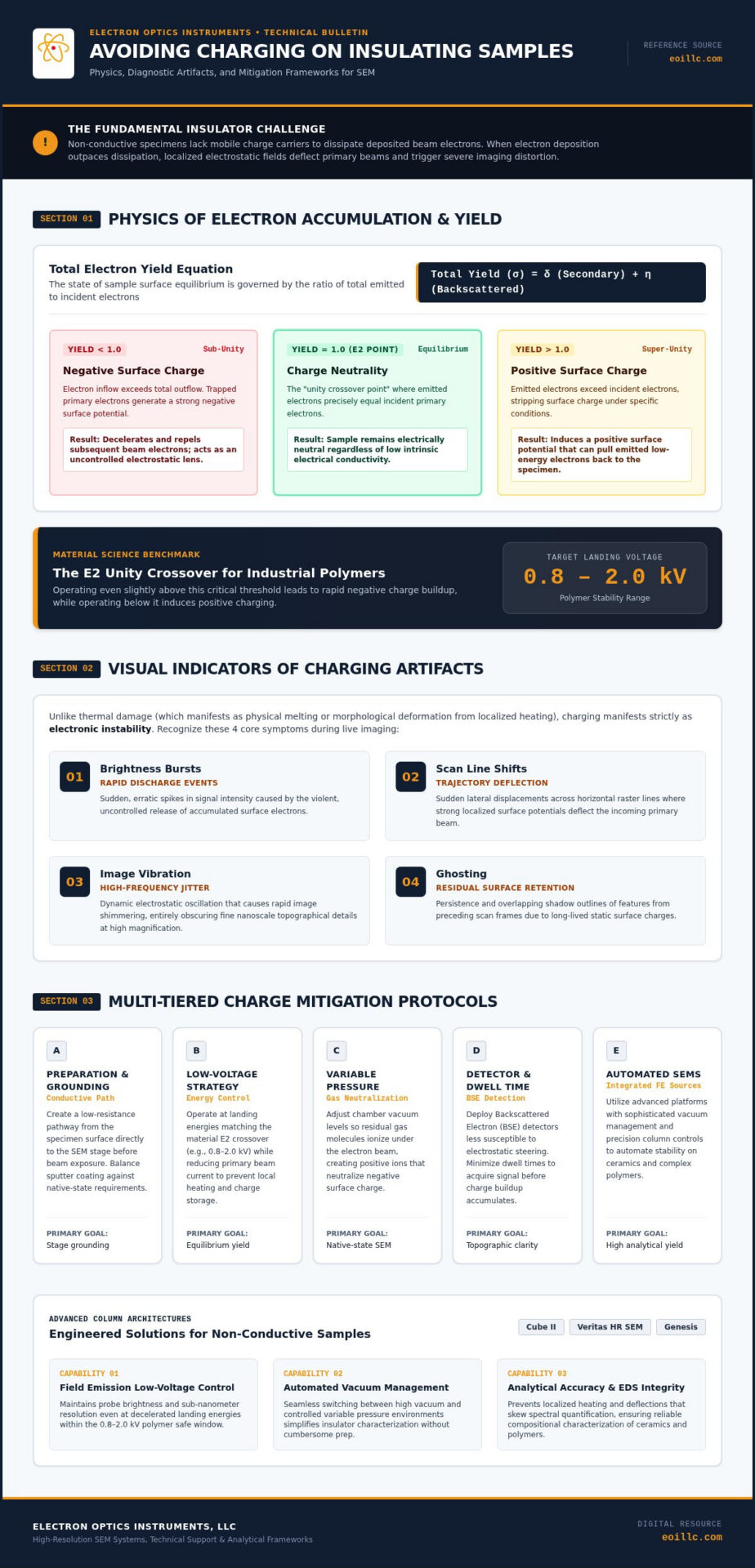
Insulating materials trap primary beam electrons within their molecular or lattice structures due to their inherent low electrical conductivity. This accumulation generates a negative surface potential that acts as a secondary electrostatic lens, often repelling or decelerating subsequent primary electrons before they even reach the sample surface. Total Electron Yield is defined as the sum of secondary and backscattered electron coefficients. If this yield remains below unity, the specimen will continue to accumulate negative charge, whereas a yield exceeding unity can, in certain conditions, induce a positive surface charge.
The Critical Energy Concept (E2)
Achieving a state of charge equilibrium requires identifying the “unity crossover point,” specifically the second critical energy point known as E2. At this specific accelerating voltage, the ratio of emitted electrons to incident electrons is exactly one, meaning the sample remains neutral regardless of its conductivity. Research indicates that for most industrial polymers, this state of charge stability is typically achieved within the 0.8 to 2.0 kV range. It’s a delicate balance; operating even slightly above this threshold leads to negative charge buildup, while operating below it can cause positive charging, both of which degrade image quality.
Visual Indicators of Charging Artifacts
Recognizing the symptoms of charging is vital for real-time instrumental adjustment. Unlike thermal damage, which results in physical melting or deformation from localized heating, charging manifests as electronic instability. Common indicators include:
- Brightness bursts: Sudden, erratic increases in signal intensity caused by rapid discharge events.
- Scan line shifts: Lateral displacements in the image where the beam has been deflected by the surface potential.
- Image vibration: High-frequency jitter that obscures fine topographical details at high magnifications.
- Ghosting: The persistence of features from previous scan frames due to residual surface charge.
Advanced ceramics and complex polymers frequently exhibit these artifacts when imaged at conventional voltages, making the transition to low-voltage or variable-pressure strategies essential for maintaining technical authority in materials characterization.
Sample Preparation Protocols to Mitigate Charge Accumulation
Achieving electrostatic equilibrium begins long before the electron beam is activated. While instrumental parameters are critical, the meticulous execution of sample preparation protocols remains the primary defense for avoiding charging on insulating samples. The objective is to establish a low-resistance path to ground, ensuring that incident electrons can migrate from the specimen surface to the SEM stage without inducing a disruptive surface potential. This NIST guide to mitigating sample charging underscores the necessity of these foundational steps for maintaining morphological integrity and analytical precision.
Sputter Coating: Gold, Platinum, and Carbon
Applying a thin conductive layer is the most reliable method for stabilizing non-conductive surfaces. For high-resolution topographic imaging, a gold or gold-palladium alloy is preferred due to its high secondary electron yield and fine grain structure. However, when elemental quantification is the priority, carbon coating is essential, as its low atomic number minimizes interference with Energy Dispersive Spectroscopy (EDS) peaks. Research suggests that a coating thickness of 2 to 5 nm is generally sufficient to prevent charging without masking critical nano-scale features. Excessive thickness can lead to artifacts or the obscuration of genuine surface details, making precise control over sputter time and vacuum levels mandatory.
Conductive Bridging and Mounting Best Practices
Proper mounting involves more than merely adhering a specimen to a stub. The distance between the region of interest and the nearest conductive path should be minimized to reduce the resistance encountered by accumulating electrons. For large or highly porous samples, creating a “grounding bridge” with high-purity silver paste or carbon paint is often necessary. This technique ensures a continuous conductive circuit from the specimen’s upper surface to the aluminum stub. For researchers who require rapid results, the Cube II Benchtop SEM provides an optimized platform for analyzing these prepared specimens with minimal downtime.
When preparing a challenging specimen, such as a ceramic pellet, follow this technical protocol to ensure a robust ground path:
- Secure the ceramic pellet to a standard aluminum stub using high-purity conductive carbon tape.
- Apply a thin, continuous line of silver paint starting from the upper perimeter of the pellet’s side wall, ensuring it does not overlap the specific region of interest.
- Extend the paint line down the side of the pellet until it makes direct contact with the aluminum stub surface.
- Allow the solvent to evaporate completely, preferably within a desiccator, to prevent vacuum contamination and outgassing during imaging.
Environmental factors also play a significant role. Biological specimens or hydrated materials must undergo thorough dehydration or critical point drying. Residual moisture or volatile compounds can lead to outgassing, which destabilizes the vacuum and exacerbates charging effects through the ionization of gas molecules in the chamber.
Optimizing Instrumental Parameters for Non-Conductive Materials
Effective characterization of non-conductive specimens requires a shift from conventional high-voltage imaging to a more nuanced manipulation of electron optics. While sample preparation provides a foundation, the active management of instrumental parameters is the decisive factor in avoiding charging on insulating samples during real-time observation. This involves a strategic recalibration of the electron beam’s energy and flux to match the specimen’s specific secondary electron emission characteristics, ensuring that the rate of electron accumulation doesn’t exceed the rate of dissipation.
The Low Accelerating Voltage Workflow
Operating below the 5 kV threshold, known as Low-Voltage SEM (LVSEM), is the most effective strategy for preserving the morphological integrity of beam-sensitive materials. By systematically decreasing the accelerating voltage, an operator can identify the specific E2 point where the number of emitted electrons equals the number of incident electrons. While theoretical models often suggest using the lowest possible voltage, practical application reveals a critical trade-off; extremely low kV settings can lead to a significant loss of resolution and a degraded signal-to-noise ratio. To counter this, advanced field emission sources, like those utilized in the Veritas HR SEM, provide up to 1,000 times more brightness than traditional tungsten filaments. This enables high-resolution imaging at landing energies as low as 1 kV, achieving the clarity necessary for nanoscale characterization without inducing surface instability.
Managing the beam current is equally vital. By selecting a smaller objective aperture and a reduced spot size, you effectively limit the electron flux hitting the specimen. This reduction in current prevents the rapid accumulation of localized charge that typically causes image blooming. Adjusting the Working Distance (WD) is also essential. A shorter WD generally improves signal collection for secondary electrons, though it may necessitate even lower voltages to maintain electrostatic equilibrium. It’s a precise balance that requires methodical adjustment to capture artifact-free data.
Variable Pressure and Low Vacuum Modes
When a sample can’t be coated or remains unstable at low voltages, Variable Pressure (VP) modes provide an indispensable alternative. This technique involves introducing a controlled amount of gas, such as air or nitrogen, into the chamber. As the electron beam passes through, it ionizes the gas molecules, creating positive ions that are attracted to the negatively charged surface of the specimen. This interaction effectively neutralizes the surface potential, allowing for stable imaging of polymers and biological tissues in their native state. For a deeper exploration of these specialized imaging modes, consult the Advanced SEM Techniques guide. The Genesis Tabletop SEM utilizes automated vacuum control to maintain these precise pressures, ensuring stable conditions for even the most challenging insulators.
Advanced Scanning Strategies and Detector Selection for Insulators
While sample preparation and voltage optimization establish the foundational conditions for imaging, the selection of detector geometry and scanning cadence represents the final layer of control in avoiding charging on insulating samples. Standard Everhart-Thornley detectors, while excellent for conductive topography, often capture the erratic signal bursts characteristic of a charged surface, leading to the brightness shifts and blooming artifacts discussed in previous sections. By moving beyond conventional secondary electron imaging, researchers can utilize advanced detection and scanning protocols to extract high-fidelity data from even the most challenging non-conductive materials.
BSE vs. SE Imaging for Non-Conductors
Backscattered Electron (BSE) detectors offer a more resilient alternative for non-conductive specimens because high-energy backscattered electrons originate from deeper within the interaction volume and possess sufficient kinetic energy to escape the localized surface potentials that trap lower-energy secondary electrons. This characteristic makes BSE imaging intrinsically more stable for compositional analysis of complex ceramics or heterogeneous polymers. By strategically optimizing the detector bias to filter out the “charged” low-energy electrons, operators ensure that only the stable, high-energy signal contributes to the final image, resulting in improved compositional contrast without the instability of topographic “ghosting.”
Scanning Speed and Image Processing
Scanning speed serves as a critical temporal variable in the management of electrostatic accumulation. A longer dwell time allows more electrons to accumulate at a single pixel, which inevitably leads to localized surface instability and image drift. Implementing a “TV Rate” or high-speed scanning strategy distributes the beam’s energy across the surface more rapidly, preventing the buildup of charge in any single coordinate. While fast scans often suffer from increased noise, modern image processing techniques, such as frame integration and recursive filtering, allow researchers to recover a high signal-to-noise ratio without re-introducing charging artifacts. Integrating these advanced scanning strategies into a standardized SEM operation workflow ensures consistent, reproducible results across varied material classes.
Tilting the specimen also serves as a strategic instrumental adjustment. By altering the incident angle of the primary beam, you increase the path length of electrons near the surface, which significantly boosts the secondary electron yield. This geometric manipulation can help push the total electron yield toward the unity crossover point, effectively neutralizing the specimen’s surface potential. For those seeking to enhance their laboratory’s technical prowess, you can schedule a technical consultation with our SEM experts to optimize your specific detector configurations and scanning workflows.
Leveraging Modern Benchtop SEM Technology for Challenging Samples
The transition from manual preparation protocols to advanced instrumental integration represents the current frontier in electron microscopy. Modern hardware, particularly the Cube II Benchtop SEM, has been engineered to streamline the process of avoiding charging on insulating samples through sophisticated vacuum management and optimized electron optics. These systems mitigate the traditional barriers to non-conductive imaging by offering a high degree of automation, allowing researchers to focus on data interpretation rather than troubleshooting electrostatic instability.
Cube II: High Performance in a Compact Footprint
The Cube II provides high performance within a compact footprint, specifically addressing the needs of industrial failure analysis and materials research. Its ability to switch seamlessly between high and low vacuum modes allows for the visualization of both coated and native-state specimens without the complexity of a full-scale field emission system. This flexibility is a cornerstone of the Desktop SEM evolution, which has redefined how laboratories approach high-resolution microscopy in 2026. By utilizing automated protocols, the system ensures that even novice users can achieve stable imaging on beam-sensitive polymers and ceramics.
In systems like the Genesis Tabletop SEM, automated vacuum control maintains the precise ionization levels required to neutralize surface charge in real-time. This is essential for maintaining analytical accuracy when using integrated EDS systems. If the surface potential isn’t stabilized, the resulting beam deflection can lead to significant errors in elemental mapping and quantitative analysis. Modern benchtop systems integrate these detectors directly into the software workflow, providing a seamless transition between topographic observation and chemical characterization.
Professional Support and Preventative Maintenance
Sustaining these high standards of accuracy requires more than just high-end hardware. Column cleanliness and vacuum integrity are vital factors in preventing artifacts. Adhering to a rigorous schedule of SEM maintenance ensures that your system operates at peak performance, minimizing the risk of contamination that can exacerbate charging. A clean column facilitates a more stable electron beam, which is a prerequisite for high-resolution work at low landing energies.
Technical excellence is ultimately anchored by the proficiency of the operator. On-site technical training ensures your team can master the technical nuances of avoiding charging on insulating samples by correctly balancing voltage, vacuum, and detector settings. This expert-driven approach, combined with the reliability of Veritas series instruments, allows for the consistent production of crisp, artifact-free images that meet the rigorous standards of international production and research environments.
Advancing Analytical Precision in Non-Conductive Microscopy
Mastery of electron optics for insulating materials requires a deliberate transition from traditional high-voltage imaging to a meticulous balance of landing energy and environmental pressure. By identifying critical crossover points and utilizing sophisticated detector strategies, researchers can effectively mitigate surface instability. Achieving consistent results in avoiding charging on insulating samples is no longer a matter of trial and error; it’s a technical discipline underpinned by precise instrumental calibration and robust preparation protocols. This synergy between hardware capability and operator expertise ensures that morphological integrity remains uncompromised during nanoscale characterization.
As the sole US distributor for EmCraft SEMs, we leverage over 30 years of technical expertise to provide comprehensive service and training for all major SEM brands. Our commitment to industrial innovation ensures that your laboratory maintains the highest standards of accuracy and reliability. Explore the Cube II Benchtop SEM for High-Resolution Imaging of Insulators to see how integrated automation can transform your characterization workflows. With the right technical framework, you’ll capture the crisp, artifact-free topographical data essential for modern industrial excellence.
Frequently Asked Questions
What is the most effective way to avoid charging on insulating samples in SEM?
The most effective method for avoiding charging on insulating samples involves a synergistic application of low accelerating voltage and meticulous sample grounding. While sputter coating remains a reliable standard for topographic stability, operating at the E2 crossover point allows for charge equilibrium without surface modification. Systems like the Veritas HR SEM facilitate this balance by providing high brightness at low energies, ensuring that the rate of electron emission matches the primary beam’s inflow.
Can I image a non-conductive sample without sputter coating?
Imaging non-conductive specimens in their native state is achievable through Variable Pressure (VP) or Environmental SEM modes. These techniques introduce a controlled gas environment to neutralize surface potentials, making them ideal for beam-sensitive polymers or biological tissues. The Cube II Benchtop SEM is specifically designed for these applications, allowing operators to bypass sputter coating while maintaining stable imaging conditions. This approach is critical for preserving original surface chemistry for subsequent analytical procedures.
How does accelerating voltage affect sample charging?
Accelerating voltage directly dictates the depth of electron penetration and the resulting secondary electron yield. At high voltages, electrons accumulate deep within the specimen, creating a negative potential that distorts the image. Conversely, reducing the voltage to the 0.8 to 2.0 kV range often achieves the unity crossover point, where the total electron yield equals the incident beam current. Finding this precise balance is a cornerstone of professional technical protocols for avoiding charging on insulating samples.
What are the visual signs that my SEM sample is charging?
Visual indicators of electrostatic accumulation include sudden brightness bursts, erratic scan line shifts, and significant image blooming. You might also observe the beam being deflected away from its intended path, resulting in ghosting or lateral displacements of topographical features. These artifacts signify that the surface potential has become high enough to interact with the primary electron column. Recognizing these signs early allows for immediate adjustments to beam current or vacuum levels.
Is low vacuum (variable pressure) always better for insulators?
Variable pressure is highly advantageous for samples that are prone to outgassing or those that don’t tolerate conductive coatings, but it isn’t a universal solution. While it effectively neutralizes charge, the presence of gas molecules can lead to beam scattering, which slightly reduces ultimate resolution compared to high-vacuum modes. For nanoscale characterization of dry ceramics, a low-voltage strategy in a high-vacuum environment, supported by a Veritas FE SEM, often provides superior topographic detail.
How does sputter coating thickness impact SEM image quality?
Coating thickness must be precisely controlled to avoid masking the very features you intend to characterize. A layer of 2 to 5 nm is typically sufficient to provide a path to ground for most insulating materials without obscuring fine morphological details. If the coating exceeds this range, the grain size of the metal can create artificial textures or hide nano-scale pores. Meticulous control of sputter time is essential for maintaining the integrity of the specimen’s original structure.
What role does the scan speed play in charge mitigation?
Scan speed functions as a temporal control for charge accumulation. By utilizing a fast scanning cadence, such as TV Rate, the electron beam spends less dwell time on each individual pixel, preventing the localized buildup of negative potential. While this may increase noise, modern frame integration techniques allow for the recovery of a high signal-to-noise ratio. This strategy is a fundamental component of the technical workflows taught during our on-site professional training sessions.
Can charging on a sample affect EDS analysis results?
Electrostatic charging significantly compromises the accuracy of Energy Dispersive Spectroscopy (EDS) by deflecting the incident beam away from the intended region of interest. This displacement leads to spatial inaccuracies in elemental mapping and quantitative errors in peak identification. A charged surface can also shift the landing energy of the primary beam, altering the excitation volume and the resulting X-ray yield. Establishing a stable conductive path is mandatory for achieving reliable analytical results.