
The traditional reliance on sputter coating for non-conductive materials often forces a compromise between electrical stability and the preservation of genuine surface morphology. While conductive layers mitigate charging, they frequently obscure the very sub-micron details that researchers must document. Utilizing low vacuum sem for non-conductive samples represents a sophisticated shift toward environmental control, where controlled gas ionization replaces the need for intrusive metallic coatings. This methodology ensures that the specimen remains in its native state, facilitating a more accurate representation of its structural and chemical identity.
You’ve likely encountered the persistent challenges of image instability, where streaks and bright spots compromise data integrity on sensitive polymers or complex biological specimens. This guide details how to master the complexities of low-vacuum technology to eliminate these charging artifacts while maintaining the sample’s pristine chemistry for Energy Dispersive Spectroscopy. We’ll examine the technical integration of variable pressure systems, such as the Veritas Series or Cube II, and how these platforms streamline laboratory workflows by bypassing the pre-treatment phase entirely to achieve superior analytical accuracy.
Key Takeaways
- Understand the principles of gas ionization and how controlled atmospheric environments neutralize surface potential to maintain sample integrity without conductive coatings.
- Optimize imaging stability by identifying the Critical Voltage (E2) where the total electron yield achieves unity on sensitive, non-conductive surfaces.
- Assess the strategic benefits of low vacuum sem for non-conductive samples, particularly for preserving native chemistry and improving the accuracy of Energy Dispersive Spectroscopy (EDS).
- Refine operational parameters, including beam current and spot size, to mitigate charge injection and prevent thermal damage to delicate specimen structures.
- Explore the technical integration of advanced platforms like the Veritas Series and Cube II to enhance analytical precision in specialized industrial and research environments.
The Physics of Electrostatic Charging in Non-Conductive SEM Samples
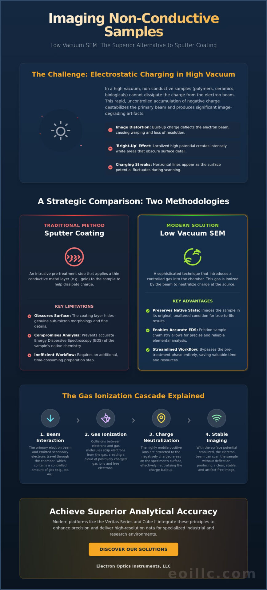
The interaction between an electron beam and a specimen surface is governed by the rigorous principle of electrostatic equilibrium. In standard scanning electron microscopy, the incident primary electrons must be balanced by the total emitted signal to prevent the accumulation of surface potential. This balance is defined by the Total Yield, which is the sum of the secondary electron yield (δ) and the backscattered electron yield (η). When this sum doesn’t equal unity, the sample begins to accumulate charge, a phenomenon that’s particularly aggressive in insulating materials. While high vacuum environments are ideal for preventing beam scattering, they provide no mechanism for charge dissipation other than a direct conductive path to the ground. Consequently, the adoption of low vacuum sem for non-conductive samples has become a critical strategy for researchers who require high-fidelity imaging without the destructive or obscuring effects of traditional sputter coating.
Identifying Charging Artifacts in Micrographs
Charging manifests through several distinct visual distortions that can be easily misinterpreted as genuine topographic features. One of the most prevalent issues is the ‘bright-up’ effect, where localized surface potential increases the emission of secondary electrons, causing certain areas to appear intensely white and devoid of detail. Unlike actual surface peaks, these anomalies often shift or change intensity as the beam dwells on the area. Additionally, periodic charging streaks frequently appear when the scan speed isn’t synchronized with the rate of charge dissipation. These horizontal lines indicate that the sample’s surface potential is fluctuating during the raster process. In extreme cases, the built-up electrostatic field becomes strong enough to cause beam deflection, resulting in significant image distortion and loss of spatial resolution.
Limitations of Conventional High Vacuum Imaging
Conventional high vacuum SEM relies on the specimen being sufficiently conductive to allow electrons to flow to the stage. Materials such as polymers, ceramics, and certain biological tissues act as electron traps due to their inherent dielectric properties. Under high vacuum, these insulators can’t shed the excess negative charge, leading to a rapid buildup that destabilizes the primary beam. This often forces operators to use lower accelerating voltages to minimize charge injection, which unfortunately limits the resolution and depth of field. The development of the Environmental Scanning Electron Microscope (ESEM) and modern variable pressure systems addressed these limitations by introducing a gaseous buffer. Without this environmental control, beam-sensitive samples often suffer irreversible structural damage before a clear image can even be captured. Modern systems like the Veritas series utilize these principles to maintain specimen integrity while delivering the high-resolution data required for advanced industrial analysis.
The Mechanics of Charge Neutralization in Low Vacuum SEM
The transition from high vacuum to a variable pressure environment represents a strategic pivot in electron microscopy, focusing on the deliberate introduction of gas molecules to mitigate electrostatic buildup. By bleeding controlled amounts of air, Nitrogen (N2), or water vapor into the specimen chamber, the system creates a medium capable of dissipating charge. This process requires a meticulous balance of pressure levels, typically ranging from 10 to 3000 Pa, to ensure that the Mean Free Path of the electron beam remains sufficient for high-resolution imaging. If the pressure is too low, charge accumulation persists; if it’s too high, excessive beam scattering, known as the ‘skirt effect,’ obscures the fine topography of the specimen. Achieving this equilibrium is fundamental to the successful implementation of low vacuum sem for non-conductive samples, where the gas itself becomes an active component of the imaging chain.
The Gas Ionization Cascade Explained
The core of the neutralization process lies in the ionization cascade, a phenomenon where the primary electron beam and emitted secondary electrons collide with gas molecules in the chamber. These collisions strip electrons from the gas atoms, creating a population of mobile positive ions and additional secondary electrons. This interaction generates a ‘plasma-like’ environment within the gap between the detector and the specimen. Because the sample surface holds a negative potential due to electron trapping, it naturally attracts these newly formed positive ions. This continuous migration effectively provides the charge neutralization in low vacuum SEM required to stabilize the surface potential. The efficiency of this cascade is directly proportional to the gas pressure and the accelerating voltage, requiring precise technical integration to maintain a stable imaging environment.
Signal Detection in Gaseous Environments
Standard Everhart-Thornley detectors are generally unsuitable for low vacuum modes because the high bias voltage required for their operation would trigger electrical arcing in a gaseous environment. Instead, specialized Gaseous Secondary Electron Detectors (GSED) leverage the ionization cascade to amplify the signal, using the gas molecules as a natural multiplier. For researchers prioritizing compositional data, Backscattered Electron (BSE) imaging often becomes the preferred modality in low vacuum settings. BSE signals possess higher energy and are less susceptible to the scattering effects of the gas, allowing for clear contrast even at higher chamber pressures. Systems like the Cube II Benchtop SEM utilize these advanced detection strategies to deliver artifact-free imaging of polymers and ceramics. By optimizing the synergy between gas pressure and detector sensitivity, these platforms preserve the signal-to-noise ratio while ensuring the native integrity of the non-conductive specimen remains uncompromised.
Strategic Comparison: Low Vacuum vs. Sputter Coating
The decision to utilize low vacuum sem for non-conductive samples instead of traditional sputter coating represents a strategic choice between absolute spatial resolution and the preservation of a specimen’s native integrity. Sputter coating remains the standard for achieving the highest possible magnifications by providing a robust conductive path, yet the application of a metallic or carbon layer can hide the very nanometer-scale surface features that researchers need to observe. Conversely, low vacuum modes maintain the specimen in its original condition, which is essential when the goal is to document true morphology without the risk of preparation-induced artifacts. This approach also enhances operational throughput by eliminating the time-intensive pre-treatment steps, allowing for immediate loading and analysis of complex specimens.
From a financial and logistical standpoint, the reliance on low vacuum technology reduces the ongoing expenditure on noble metal targets and specialized coating consumables. While high-vacuum imaging with a conductive coat is effective for routine inspections, the total cost of ownership for a laboratory often improves when utilizing a versatile platform like the Veritas Plus SEM, which handles diverse material types without secondary processing. The ability to bypass the sputter coater not only saves on material costs but also reduces the potential for sample contamination or structural damage during the coating process.
Preserving Native Chemistry for EDS Analysis
Analytical accuracy in Energy Dispersive Spectroscopy (EDS) is frequently compromised by the presence of conductive coatings. Gold, platinum, or carbon targets generate characteristic X-ray peaks that can overlap with the signals of interest, complicating the deconvolution of complex spectra. By opting for low vacuum modes, researchers achieve quantitative elemental mapping that reflects the true stoichiometry of the material. This ensures that light elements, such as carbon or oxygen, are detected without the interference of an artificial surface layer, providing higher confidence in the resulting data for geological or biological research.
Choosing the Right Method for Your Material Class
The choice of methodology is dictated by the specific material class under investigation. For polymers and textiles, low vacuum is often superior because it provides simultaneous charge neutralization and heat dissipation, preventing beam-induced melting. In contrast, semiconductor failure analysis often requires the extreme resolution of high-vacuum imaging, making a thin conductive coat necessary. For ceramics and geological samples, the ability of low vacuum sem for non-conductive samples to handle porous and irregular surfaces without the need for a uniform coating makes it the preferred strategic option for comprehensive topographic and chemical characterization.
Optimizing SEM Parameters for Non-Conductive Imaging
Achieving electrostatic equilibrium on an insulating surface necessitates a meticulous calibration of primary beam parameters that extends beyond basic hardware settings. When utilizing low vacuum sem for non-conductive samples, the operator must synchronize the rate of electron injection with the rate of dissipation provided by the gaseous environment. This involves a precise adjustment of the spot size and beam current to minimize the volume of charge introduced to the specimen. High beam currents, while beneficial for signal-to-noise ratios, often lead to rapid dielectric breakdown and localized heating. By reducing the probe current and optimizing the convergence angle, researchers can maintain stable imaging conditions even on the most challenging polymeric or ceramic substrates.
Accelerating Voltage and the E2 Point
The Critical Voltage, or E2 point, represents the specific energy level where the total electron yield exactly equals unity. At this equilibrium, the number of secondary and backscattered electrons leaving the sample matches the number of primary electrons entering it, effectively preventing surface potential buildup. Finding this point is a dynamic process that varies based on the material’s atomic number and surface geometry. Modern desktop SEM systems have revolutionized this workflow by offering automated low-voltage optimization routines. These platforms allow users to operate at voltages below 5 kV, where many non-conductive materials naturally reach their E2 point, thus preserving the sample’s native state without the need for complex pre-treatment protocols.
Pressure Control and Signal Amplification
Selecting the appropriate chamber pressure is a balancing act between charge neutralization and beam stability. While a range of 10 to 100 Pa is typical for most low vacuum sem for non-conductive samples, the minimum pressure required for stability should always be prioritized to mitigate the ‘skirt’ effect. This phenomenon occurs when gas molecules scatter the primary beam, creating a broad halo of electrons that reduces image contrast and spatial resolution. High-sensitivity Backscattered Electron (BSE) detectors are particularly effective in these environments, as their high-energy signal remains relatively unaffected by the gaseous medium. To achieve the highest fidelity in your analysis, consider upgrading your laboratory with the Veritas HR SEM, which features advanced pressure regulation and high-contrast detection systems designed for demanding industrial applications.
The final pillar of optimization is the synergy between scan speed and charge dissipation. Rapid scanning can often ‘outrun’ the accumulation of charge, but it may also introduce stochastic noise that obscures fine detail. Conversely, slow scan speeds allow for better signal integration but increase the risk of localized charging. Effective imaging requires the operator to find a temporal middle ground where the ionization cascade in the chamber can effectively neutralize the surface potential between each raster line. This methodical approach ensures that every micrograph produced is a true representation of the specimen’s topography and composition.
Advanced Low Vacuum Solutions from Electron Optics Instruments
The transition from theoretical optimization to empirical results requires hardware that’s meticulously engineered for precision under variable pressure environments. Electron Optics Instruments provides a comprehensive suite of systems specifically configured for low vacuum sem for non-conductive samples, ensuring that laboratories can achieve high-fidelity imaging without the structural or chemical limitations of sputter coating. From the compact efficiency of the Cube II to the research-grade performance of the Veritas Ultra SEM, these platforms integrate advanced gaseous secondary electron detection with robust vacuum control systems. This equipment allows researchers to maintain the native integrity of their specimens while accessing the high-resolution data necessary for sophisticated industrial analysis.
Leveraging the Cube II for Insulating Samples
The Cube II Benchtop SEM serves as a primary example of how automated pressure management can streamline complex laboratory workflows. It features a sophisticated interface that allows for rapid toggling between high and low vacuum modes, making it an ideal solution for the high-throughput analysis of insulating polymers, textiles, and ceramics. Its high-brightness electron source ensures that signal intensity remains superior even when navigating the scattering effects inherent in a gaseous environment. This technical synergy allows for a compact footprint that doesn’t sacrifice the analytical depth required for modern quality control, providing a visionary approach to benchtop microscopy.
For organizations requiring scalable performance, the Veritas Series SEM offers a developmental path from routine inspection to high-resolution research. These systems, including the Veritas Pro and Veritas HR SEM, can be customized with high-sensitivity EDS Systems to facilitate simultaneous topographic and compositional analysis. By leveraging the low vacuum capabilities of the Veritas FE SEM, users can perform quantitative elemental mapping on uncoated specimens with unprecedented accuracy. This integration of hardware and spectroscopy ensures that the synergy between industrial performance and analytical precision is maintained across all levels of production and logistical excellence.
Expert Support and Maintenance for Peak Performance
Sustaining the precision of these advanced hardware systems requires a commitment to rigorous SEM maintenance, particularly concerning the integrity of variable pressure seals and vacuum pumps. Beyond hardware, Electron Optics Instruments offers tailored on-site training to help your team master advanced SEM techniques, ensuring that every operator can maximize the potential of the low-vacuum environment. Our national service network provides the stability and thoroughness expected from a global innovator, offering everything from Preventative Maintenance Visits to the supply of high-quality SEM Filaments and Consumables. We also provide Refurbished SEM Units for institutions seeking to integrate low-vacuum capabilities within specific budgetary frameworks, ensuring that superior standards are accessible across the specialized industrial sector.
Advancing Analytical Precision through Environmental Control
Integrating low vacuum sem for non-conductive samples into your laboratory workflow represents a fundamental advancement in material characterization. By mastering the delicate balance of gas ionization and primary beam parameters, researchers can successfully bypass the structural and chemical limitations of traditional sputter coating. This technical evolution ensures that the native topography and elemental stoichiometry of sensitive specimens remain uncompromised, delivering the rigorous data required for specialized industrial sectors. It’s a strategic shift that prioritizes analytical accuracy without sacrificing operational efficiency.
Electron Optics Instruments brings over 30 years of specialized electron optics expertise to your facility as the exclusive US distributor for EmCraft SEMs. Our commitment to technical excellence extends beyond high-end hardware to include nationwide on-site technical training and a comprehensive service network. Explore the Cube II Benchtop SEM for your non-conductive imaging needs and secure the analytical stability your research demands. With the right technical partnership, achieving artifact-free imaging of your most complex materials becomes a routine reality.
Frequently Asked Questions
What is the primary advantage of low vacuum SEM for non-conductive samples?
The primary advantage is the ability to image specimen surfaces in their native state by eliminating the requirement for conductive sputter coatings. This methodology prevents the obscuration of fine topographic details and ensures that the sample’s chemical profile remains unaltered for subsequent analysis. Utilizing low vacuum sem for non-conductive samples facilitates immediate observation of insulating materials without the risk of preparation-induced artifacts.
Does low vacuum SEM affect the resolution of my images?
Low vacuum imaging can result in a slight reduction in spatial resolution due to the scattering of the primary electron beam by gas molecules, often referred to as the skirt effect. However, modern electron optics and high-sensitivity detectors significantly mitigate this loss. By optimizing the Mean Free Path and using lower accelerating voltages, researchers achieve high-fidelity images that are sufficient for the vast majority of industrial and research applications.
Can I perform EDS analysis while in low vacuum mode?
Energy Dispersive Spectroscopy (EDS) analysis is not only possible but frequently more accurate in a low vacuum environment. Because there is no metallic coating to generate interfering X-ray peaks, the resulting spectra represent the true elemental stoichiometry of the specimen. This is particularly critical for the detection of light elements in complex geological or biological matrices where coating overlaps would otherwise compromise data integrity.
What types of samples are best suited for low vacuum imaging?
This technology is best suited for materials with high dielectric constants that act as electron traps under high vacuum conditions. Common examples include technical ceramics, synthetic polymers, textiles, and porous geological specimens. It’s also ideal for beam-sensitive biological samples that might suffer thermal or structural damage if subjected to the coating process or high-energy electron bombardment in a standard vacuum.
How do I determine the correct chamber pressure for my sample?
The optimal chamber pressure is the minimum value required to achieve charge neutralization, which typically falls between 10 Pa and 150 Pa for most specimens. Operators should start at a lower pressure and incrementally increase it until the visual artifacts of charging, such as streaks or bright spots, disappear. Excessive pressure should be avoided as it increases beam scattering and reduces the signal-to-noise ratio.
Is a special detector required for low vacuum SEM imaging?
Specialized detectors are necessary because standard Everhart-Thornley detectors cannot operate at the high bias voltages required in a gaseous environment without risking electrical arcing. Low vacuum systems utilize Gaseous Secondary Electron Detectors (GSED) or high-sensitivity Backscattered Electron (BSE) detectors. These components are specifically engineered to leverage the ionization cascade within the chamber to amplify the imaging signal.
How does low vacuum SEM prevent sample damage?
Charge neutralization prevents the buildup of localized electrostatic fields that can cause dielectric breakdown or mechanical stress within the specimen. Additionally, the presence of gas molecules provides a medium for convective heat dissipation, which protects sensitive polymers and biological tissues from beam-induced melting. This environmental control ensures that the sample remains structurally intact throughout the duration of the analysis.
Can I switch between high vacuum and low vacuum modes on the Cube II?
The Cube II Benchtop SEM features a sophisticated, automated interface that allows for rapid switching between high vacuum and low vacuum modes. This flexibility enables users to perform routine high-resolution imaging on conductive samples before transitioning to variable pressure for insulating materials. It’s a technical integration designed to maximize laboratory throughput by accommodating a wide range of specimen types on a single, compact platform.