
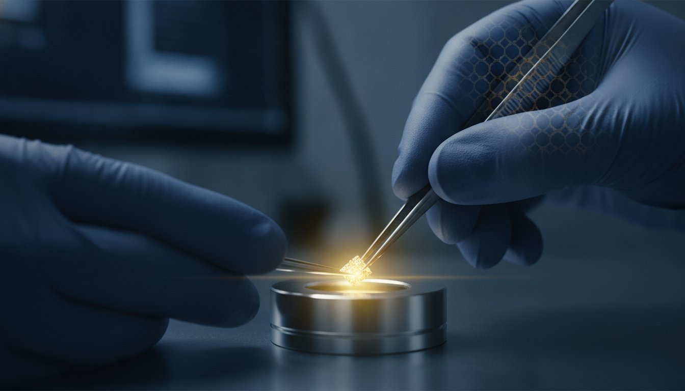
The ultimate resolution of your scanning electron microscope is determined long before the electron beam ever strikes the surface of your specimen. While sophisticated hardware like the Cube II Benchtop SEM offers remarkable precision, the integrity of your final data depends entirely on the methodological rigor applied during the initial stages of setup. Many researchers struggle with persistent image charging and the catastrophic loss of morphological detail. These frustrations often stem from a lack of standardized sem sample preparation techniques that account for the unique requirements of high-vacuum environments.
You recognize that consistent, high-contrast imaging is the cornerstone of reliable industrial and academic research. This guide serves as a comprehensive resource for mastering the protocols necessary to eliminate artifacts and prevent sample contamination. We’ll examine advanced workflows for mounting, conductive coating, and specimen stabilization. By adopting these expert-level methodologies, you’ll ensure that your Veritas Series SEM operates at its peak performance, delivering the crisp, repeatable results your critical projects demand.
Key Takeaways
- Understand the fundamental requirements for specimen compatibility within high-vacuum environments to preserve the structural integrity of your samples.
- Learn to utilize specialized sem sample preparation techniques such as magnetron sputter coating to eliminate surface charging and enhance image contrast.
- Differentiate between chemical cleaning protocols and conductive coating methods to select the optimal workflow for Energy Dispersive Spectroscopy.
- Implement precise cross-sectioning and stabilization strategies for industrial failure analysis and the characterization of porous ceramic materials.
- Master the troubleshooting of common artifacts like sample drifting and “glowing” edges to maximize the high-resolution capabilities of your Cube II Benchtop SEM.
The Fundamentals of SEM Sample Preparation
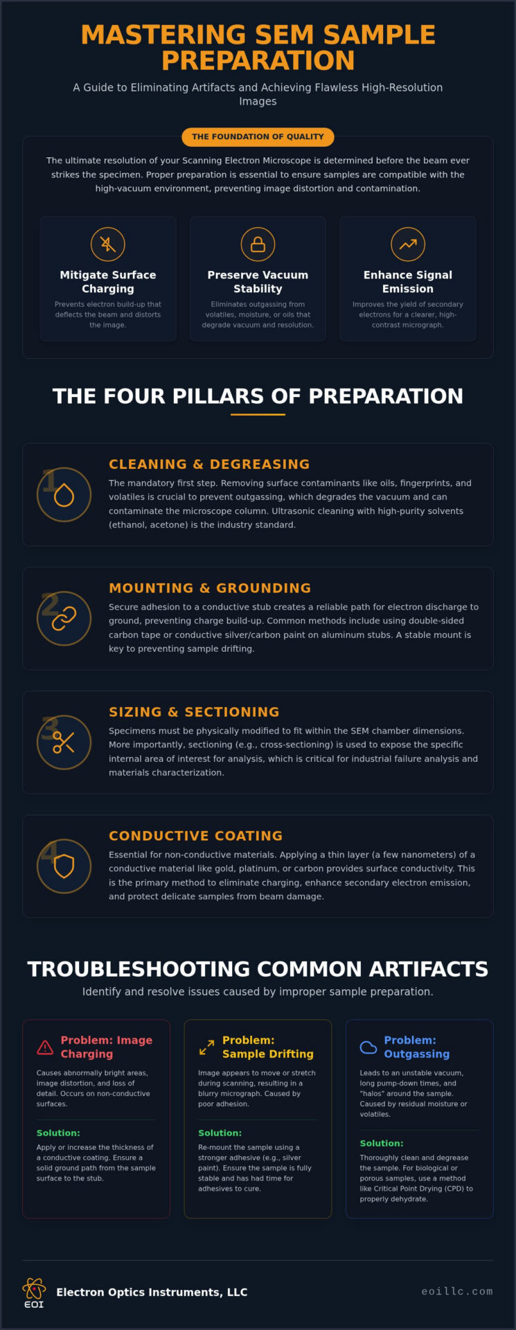
The process of scanning electron microscopy requires a specimen to exist within a high-vacuum environment while being subjected to a high-energy electron beam; consequently, sem sample preparation techniques serve as the essential bridge between the raw state of a material and its digital representation. This phase involves a series of meticulous mechanical and chemical modifications designed to ensure that the specimen is compatible with the interior of systems like the Cube II Benchtop SEM. The primary objectives of this preparation are threefold: the mitigation of surface charging, the preservation of vacuum stability, and the enhancement of secondary electron emission. Failure to adhere to these rigorous standards often results in degraded image resolution and can potentially compromise the longevity of the microscope’s vacuum system through outgassing or contamination.
Why Specimen Preparation Dictates Image Quality
Surface conductivity remains the most critical factor in achieving high-fidelity micrographs. Without a clear path for electrons to dissipate, the “charging” effect occurs, leading to the deflection of the primary beam and severe image distortion. Professional preparation also ensures that the specimen maintains its structural integrity when exposed to the thermal and electrical stresses of electron bombardment. In 2026, the distinction between benchtop and floor-model vacuum capabilities has narrowed, yet the requirement for low-outgassing samples remains absolute for maintaining sub-nanometer resolution. To explore the broader context of these interactions, researchers should review The Fundamental Principles of Scanning Electron Microscopy (SEM) in 2026.
The Four Pillars of Successful Preparation
Achieving superior results across the Veritas Series SEM line requires a systematic approach to the four pillars of preparation, integrating advanced sem sample preparation techniques into a repeatable laboratory workflow. Each stage is designed to address specific physical constraints of the electron optics environment.
- Cleaning and Degreasing: Removing oils, fingerprints, and volatiles is mandatory to prevent outgassing, which would otherwise degrade the vacuum and contaminate the column.
- Mounting and Grounding: Proper adhesion to a conductive stub using carbon tape or silver paint ensures a reliable path for electron discharge to the ground.
- Sizing and Sectioning: Specimens must be physically modified to fit within the chamber dimensions while exposing the specific area of interest.
- Conductive Coating: For non-conductive materials, the application of a thin metallic or carbon layer is necessary to provide the surface conductivity required for high-resolution imaging.
Mechanical and Chemical Preparation Protocols
Precision imaging requires an uncompromising commitment to surface purity and geometric accuracy. Even trace quantities of oils or moisture can lead to catastrophic outgassing within the vacuum chamber, resulting in column contamination and degraded resolution. Implementing standardized sem sample preparation techniques, such as the use of diamond saws for precise cross-sectioning or ultramicrotomes for delicate layering, ensures that your specimen is ready for the rigors of high-vacuum analysis. By removing surface debris and ensuring structural stability, you provide the foundation for the high-end quality expected from the Veritas Series SEM.
Degreasing and Dehydration Workflows
For metallic and ceramic specimens, ultrasonic cleaning is the industry standard for removing machining oils and fingerprints. The process typically involves immersion in high-purity solvents such as ethanol or acetone, depending on the material’s chemical resistance. Acetone provides superior degreasing for robust industrial components, while ethanol is often preferred for sensitive substrates. For delicate biological or porous structures, Critical Point Drying (CPD) is necessary to transition the sample from a liquid to a gaseous state without the surface tension effects that cause structural collapse. It’s vital to recognize that residual moisture can extend pump-down times and introduce instabilities in systems like the Cube II Benchtop SEM.
Mounting and Adhesive Selection
Selecting the appropriate mounting substrate and adhesive is a critical step in establishing a stable conductive path. Aluminum stubs are the most common choice due to their cost-effectiveness and compatibility with most SEM stages, though brass stubs may be utilized for specific high-stability applications. It’s essential to ensure a clear ground from the specimen surface to the stub to prevent the charging artifacts discussed in the previous section. Adhesive selection depends on the required throughput and the nature of the specimen:
- Double-Sided Carbon Tape: Ideal for rapid mounting of multiple small samples, providing adequate conductivity for general imaging.
- Colloidal Silver Paint: Offers superior electrical contact and mechanical stability, particularly for large or irregularly shaped specimens.
- Conductive Epoxies: Used for permanent mounting where high-strength bonding and maximum conductivity are paramount.
Achieving repeatable results in a high-volume laboratory requires a mastery of these foundational steps. For organizations looking to refine their internal workflows, on-site technical training provides an expert-driven approach to optimizing specimen preparation for any industrial application.
Conductive Coating Techniques: Sputtering vs. Evaporation
The application of a conductive thin film is the definitive stage in sem sample preparation techniques for non-conductive specimens. This process mitigates the accumulation of static electric charge, which would otherwise deflect the primary electron beam and obscure critical topographical details. Magnetron sputter coating remains the primary methodology for routine imaging, utilizing ionized gas to dislodge metallic atoms from a target and deposit them onto the specimen in a uniform layer. Achieving an industry-standard thickness between 5nm and 20nm is essential for most applications; a layer that’s too thin fails to prevent charging, while an excessive deposition risks masking nanometer-scale features. The selection of the coating material is a strategic decision that balances grain size, secondary electron yield, and operational costs.
Sputter Coating: Gold, Platinum, and Palladium
Gold is the most frequently utilized target material for standard secondary electron imaging due to its high conductivity and superior electron yield. However, for high-resolution applications using systems like the Veritas HR SEM, the relatively large grain size of gold can become visible at extreme magnifications. In these instances, platinum, iridium, or palladium-gold alloys are preferred for their significantly finer grain structures. Managing thermal energy during the sputtering process is a critical consideration for sensitive polymers or biological samples. Implementing pulsed sputtering cycles or utilizing a cooled stage prevents the specimen from undergoing thermal deformation during the deposition process, ensuring the integrity of the underlying morphology isn’t compromised.
Carbon Coating for Analytical Microscopy
While metallic coatings excel at enhancing topography, they often introduce spectral interference during elemental analysis. Carbon evaporation is the mandatory protocol when utilizing Energy Dispersive Spectroscopy (EDS) systems. Because carbon has a low atomic number, it doesn’t mask the X-ray signals from the underlying sample, ensuring accurate elemental quantification and mapping. This process involves passing a high current through a carbon thread or rod under vacuum, causing the carbon to evaporate and condense onto the specimen surface. In complex failure analysis, a dual-coating approach, applying a thin carbon layer followed by a flash of gold, can sometimes provide the optimal balance of conductivity and analytical clarity for the most demanding research environments.
Specialized Preparation for Industrial Applications
Industrial environments require specialized sem sample preparation techniques to reveal subsurface defects and characterize complex material interfaces with high-end precision. In failure analysis, the ability to perform meticulous cross-sectioning allows engineers to identify internal voids, cracks, or delamination within multi-layer electronic components. Geological and ceramic specimens present unique challenges due to their inherent porosity and lack of conductivity. These materials often require resin embedding and vacuum impregnation to prevent outgassing and ensure structural stability during high-vacuum analysis. For a deeper analysis of these methodologies, consult our guide on Advanced SEM Techniques: A Comprehensive Guide to High-Resolution Analytical Microscopy in 2026.
Cross-Sectional Polishing and Ion Milling
Achieving a deformation-free surface is paramount for Electron Backscatter Diffraction (EBSD) and the characterization of thin-film stacks. While mechanical polishing provides a preliminary finish, Argon ion milling is the preferred method for removing the amorphous “smear” layer introduced by abrasive preparation. This technique utilizes a focused beam of ions to strip away material at a molecular level, producing the mirror finish necessary for high-accuracy crystallography. In metallurgical applications, this level of precision ensures that grain boundaries and phase distributions are characterized without preparation-induced artifacts, rewarding the user with the high-resolution results typical of the Veritas Series SEM.
Handling Non-Conductive and Beam-Sensitive Samples
When samples cannot be coated or are susceptible to thermal degradation, Variable Pressure (VP) or low-vacuum modes provide a viable alternative for maintaining specimen integrity. These modes utilize a controlled atmosphere within the chamber to neutralize charge through gas ionization, allowing for the inspection of polymers and biological tissues in their native state. Charging is the accumulation of negative electrostatic potential on a non-conductive surface that deflects the primary electron beam, though it can be mitigated through the strategic application of conductive bridges or silver paint paths. For sensitive materials, integrating a cold stage with low-voltage imaging on systems like the Cube II Benchtop SEM preserves morphology under high-energy bombardment.
If your laboratory requires high-resolution data from complex industrial materials, consider our on-site technical training to refine your internal preparation protocols and maximize your hardware investment.
Troubleshooting Preparation Artifacts in Benchtop SEM
The deployment of compact systems like the Cube II Benchtop SEM has democratized high-resolution imaging across diverse industrial sectors; however, these instruments require a high degree of methodological rigor in sample handling. Common artifacts such as “glowing” edges, dark contamination spots, or sample drifting often indicate specific failures in the initial sem sample preparation techniques. While the hardware manages the electron optics with precision, the user remains responsible for the physical state of the specimen. Regular maintenance of preparation equipment, including the cleaning of sputter coater targets and the replacement of polisher abrasives, is essential to prevent the introduction of foreign debris into the vacuum chamber. For a broader understanding of instrument parameters, refer to our SEM Operation: The Professional Guide to Scanning Electron Microscopy in 2026.
Identifying and Eliminating Charging
A sudden shift in the image or a localized, uncontrollable increase in brightness usually signals a breakdown in the conductive path. These visual indicators of charging occur when the primary beam’s electrons accumulate on the surface rather than discharging to the ground. Corrective actions should be methodical. First, inspect the grounding path from the sample surface to the microscope stage. If the path is interrupted, adding a small amount of silver dag or a conductive bridge can restore the connection. If the charging persists, the specimen may require re-coating with a thicker metallic layer or a reduction in the accelerating voltage to minimize the interaction volume. Ensuring the stub is securely fastened to the stage is a simple but frequently overlooked step in maintaining electrical continuity.
Maximizing Benchtop SEM Utility Through Prep
Users of benchtop systems must be exceptionally disciplined regarding sample cleanliness due to the smaller vacuum volumes characteristic of these units. Residual moisture or trace oils can cause significant pump-down delays and lead to the formation of dark carbon spots under the beam’s path. Contamination in a benchtop system is often more localized and severe than in larger chambers. Training your team through professional SEM training is the most effective way to reduce downtime and ensure data quality remains consistent across different operators. Before inserting a sample into a benchtop system, use this final checklist to ensure optimal performance:
- Dehydration: Confirm the sample is completely dry to prevent vacuum instabilities.
- Surface Purity: Verify the absolute removal of machining oils or fingerprints.
- Conductivity: Test the grounding path from the specimen’s top surface to the aluminum stub.
- Coating Integrity: Ensure a uniform 5-20nm coating layer for all non-conductive materials.
Mastering these sem sample preparation techniques ensures that your Genesis Tabletop SEM or Cube II unit delivers the high-contrast, repeatable data required for sophisticated industrial characterization.
Elevating Imaging Standards Through Methodological Excellence
The attainment of superior resolution in scanning electron microscopy is inextricably linked to the rigor of your initial laboratory protocols. By mastering advanced sem sample preparation techniques, researchers can navigate the complexities of vacuum stability and surface conductivity to ensure that every micrograph reflects the true morphology of the specimen. Whether you’re managing industrial failure analysis or academic material characterization, the transition from raw material to precise digital data requires a disciplined adherence to cleaning, mounting, and conductive coating standards.
Electron Optics Instruments, LLC leverages over 30 years of technical authority to support laboratories in achieving these superior standards. Beyond providing high-performance hardware, we offer expert repair and preventative maintenance for all SEM brands and deliver comprehensive on-site technical training for laboratory staff to optimize internal workflows. Maximize your imaging precision with the Cube II Benchtop SEM and expert on-site training. With the right methodologies in place, your facility is positioned to push the boundaries of what’s possible in modern microscopy.
Frequently Asked Questions
Do all SEM samples need to be conductive?
Not every specimen requires inherent conductivity, but non-conductive materials must be managed through specific sem sample preparation techniques to prevent charging. While metals are naturally conductive, polymers and ceramics often require a thin metallic or carbon coating. Alternatively, systems like the Veritas Series SEM can operate in variable pressure modes to neutralize surface charge without coating. Failure to address conductivity leads to beam deflection and significant loss of topographical detail.
How do I choose between gold and carbon coating?
The choice depends on your primary research objective. Gold provides a superior secondary electron yield, making it ideal for high-resolution topographical characterization. Conversely, carbon is the mandatory choice for Energy Dispersive Spectroscopy (EDS) because its low atomic number minimizes X-ray absorption and peak interference. If your workflow requires both high-resolution imaging and elemental mapping, a dual-coating approach or a thin platinum layer may be necessary to achieve balanced results.
What happens if I put a wet or oily sample in the SEM?
Inserting wet or oily specimens into a high-vacuum chamber leads to rapid outgassing, which prevents the system from achieving its operational vacuum level. This process introduces volatiles into the column, leading to the contamination of the electron optics and potential damage to the filaments. In compact systems like the Cube II Benchtop SEM, these contaminants can quickly degrade image resolution and increase the frequency of required preventative maintenance visits to restore peak performance.
How thick should the sputter coating be for high-resolution imaging?
For most high-resolution applications, a coating thickness between 5nm and 20nm is considered the industry standard. A layer thinner than 5nm may not provide a continuous conductive path, resulting in persistent charging artifacts. If the coating exceeds 20nm, it risks obscuring the nanometer-scale surface features you intend to characterize. Achieving this precise thickness requires a calibrated sputter coater and a methodical approach to deposition timing and plasma current.
Can I use a benchtop SEM for biological samples?
Biological specimens can be successfully imaged using a benchtop SEM, provided they undergo rigorous dehydration and stabilization. Techniques such as critical point drying are essential to prevent structural collapse during the transition to a vacuum environment. Once dried, these samples are typically coated with gold or palladium to ensure conductivity. Professional on-site technical training can help your laboratory staff master these specific protocols to maximize the utility of the Genesis Tabletop SEM.
What is the best way to clean a metallic sample for SEM?
Metallic specimens should be cleaned using ultrasonic agitation in high-purity solvents to ensure the removal of all industrial contaminants. Acetone is highly effective for removing machining oils, while a subsequent ethanol rinse removes any residual solvent films. This meticulous cleaning prevents the formation of dark carbonaceous deposits under the electron beam. For specimens with complex geometries, ensuring all internal pores are free of trapped solvents is critical for maintaining vacuum stability.
How does sample preparation affect EDS analysis results?
Sample preparation is the most significant factor in achieving accurate elemental quantification. Topographical irregularities can cause X-ray shadowing, while metallic coatings like gold can overlap with critical characteristic peaks of elements like sulfur or molybdenum. Utilizing carbon evaporation as part of your sem sample preparation techniques ensures that the EDS detector receives a clear signal from the substrate without spectral interference, resulting in more reliable stoichiometric data and elemental maps.
Is ultrasonic cleaning always necessary before SEM imaging?
While ultrasonic cleaning is a standard protocol for robust industrial components, it isn’t always mandatory for every specimen type. Delicate structures or loosely adhered particles may be dislodged or destroyed by the mechanical energy of the ultrasonic bath. In such cases, gentle rinsing or dry gas cleaning may be more appropriate. The decision should be based on the physical durability of the sample and the specific level of surface contamination that must be removed.