
What if the primary bottleneck in your 2026 production cycle isn’t a supply chain disruption, but the literal invisibility of material defects at the sub-nanometer scale? As semiconductor architecture moves toward 2-nanometer processes, the necessity for a high-performance sem tool has transitioned from a laboratory luxury to a fundamental industrial requirement. You’ve likely found that the distinction between digital marketing software and precision scientific hardware is often blurred in search results, creating unnecessary friction in your procurement process. We understand that balancing the demand for ultra-high resolution with the physical limitations of benchtop space remains a persistent challenge for modern facilities.
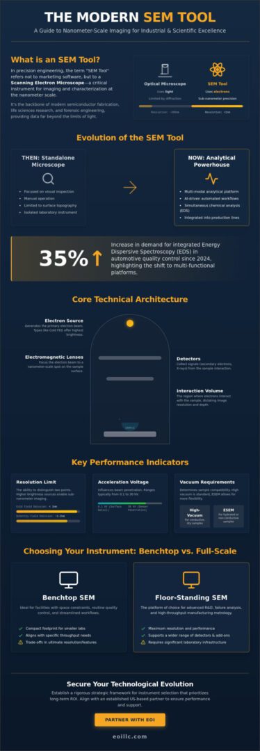
This comprehensive guide details the technical architecture and industrial applications of modern scanning electron microscopy, providing a rigorous framework for evaluating equipment performance and EDS integration. Since 2024, the demand for integrated Energy Dispersive Spectroscopy has risen by 35% in automotive quality control, highlighting the need for multi-functional analytical platforms. We’ll explore the strategic selection criteria necessary to maintain global manufacturing excellence and ensure sustainable innovation in your research workflows. By the conclusion, you’ll possess a clear understanding of hardware categories and the advantages of aligning with an established US-based partner like EOI LLC to secure your technological evolution.
Key Takeaways
- Examine the evolutionary technical architecture of the modern sem tool, emphasizing how integrated electron columns and vacuum systems facilitate high-precision imaging at the nanometer scale.
- Evaluate the spatial and operational trade-offs between benchtop and floor-standing units to ensure your laboratory infrastructure aligns with specific throughput and resolution requirements.
- Discover how AI-driven image analysis and automated workflows are revolutionizing critical dimension metrology and failure analysis within advanced manufacturing environments.
- Establish a rigorous strategic framework for instrument selection that prioritizes long-term ROI through a balance of technical performance and comprehensive preventative maintenance protocols.
Defining the SEM Tool in Scientific and Industrial Contexts
The term “sem tool” frequently creates a linguistic overlap between digital marketing suites and advanced industrial hardware. Within the context of precision engineering and materials science, however, the sem tool represents a critical instrument for nanometer-scale imaging and characterization. Unlike optical microscopes that are limited by the diffraction of light, a Scanning electron microscope utilizes a focused beam of electrons to interact with atoms in a sample, producing signals that contain detailed information about the specimen’s surface topography and composition. This technology has transitioned from a standalone laboratory microscope into a comprehensive analytical platform. By 2026, these systems integrate multiple detectors and automated workflows to serve as the backbone of semiconductor fabrication, life sciences research, and forensic engineering.
The evolution of this equipment reflects a broader shift toward integrated metrology. While early models focused primarily on visual inspection, contemporary platforms operate as multi-modal stations. They’re capable of performing simultaneous chemical analysis and structural mapping. This transition is driven by the need for sub-nanometer precision in sectors where a single defect can compromise an entire production batch. In forensic engineering, for instance, the ability to identify microscopic fatigue cracks or elemental contaminants is vital for determining the root cause of component failure in automotive or aerospace systems.
The SEM Tool as an Analytical Powerhouse
Modern platforms function as analytical powerhouses by merging electron optics with advanced digital signal processing to facilitate high-throughput data acquisition. These systems don’t just capture images; they provide quantitative data on crystallographic information and elemental distribution. In the semiconductor industry, the preference for the word “tool” over “microscope” reflects the equipment’s role in metrology and failure analysis within automated production lines. In these environments, the sem tool is a calibrated piece of capital equipment essential for maintaining yield rates in 2nm and 3nm logic node manufacturing. The integration of Energy Dispersive X-ray Spectroscopy (EDS) allows for real-time composition analysis, transforming a simple imaging device into a laboratory-on-a-chip interface.
Key Performance Indicators for SEM Hardware
Performance evaluation of these platforms depends on several key indicators, primarily the resolution limits dictated by the electron source type. Schottky field emission sources offer a balance of stability and brightness, while cold field emission sources provide the highest brightness for sub-nanometer imaging. SEM tool resolution is the ability to distinguish two points at the nanometer scale. While magnification ranges can exceed 1,000,000x, the effective field of view must be balanced against the signal-to-noise ratio to ensure data integrity during large-area mapping. Engineers must also consider the following parameters when selecting a platform:
- Acceleration Voltage: Typically ranging from 0.1 to 30 kV, influencing beam penetration and sample damage.
- Probe Current: Critical for determining the speed of analysis and the quality of chemical mapping.
- Vacuum Requirements: High-vacuum vs. environmental SEM (ESEM) capabilities for hydrated or non-conductive samples.
Core Components and Technical Architecture of Modern SEM Tools
The architectural integrity of a modern sem tool relies upon the precise orchestration of the electron column, where electromagnetic lenses focus the primary beam with nanometer-scale accuracy. This column functions as the central nervous system of the platform, directing electrons from the source through a series of apertures and scanning coils. The synergy between the primary electron beam and the sample surface creates a specific interaction volume that dictates the resolution and depth of the resulting image. This volume remains a critical variable, as it’s influenced by both the accelerating voltage and the atomic density of the specimen being analyzed.
Maintaining a rigorous vacuum environment is essential for operational stability. High-end systems typically require a vacuum level exceeding 10⁻⁶ Torr in the gun chamber to prevent gas molecule scattering and protect the emitter from ion bombardment. Research published in April 2025 by the National Institute of Standards and Technology focuses on Improving SEM Measurement Accuracy to address the inherent uncertainties in 3D topography and dimensional metrology. This level of precision is vital for the evolutionary progress of semiconductor manufacturing and materials science where sub-nanometer tolerances are now standard.
The Electron Source: Thermionic vs. Field Emission
Selecting an electron source involves a strategic evaluation of brightness and lifecycle costs. Traditional Tungsten filaments operate through thermionic emission at approximately 2,800 Kelvin, offering a cost-effective solution for routine imaging but requiring replacement every 100 to 200 hours. In contrast, Schottky Field Emission (FE) sources provide a brightness level 1,000 times greater than Tungsten, facilitating high-resolution imaging at lower accelerating voltages. While the initial capital expenditure for an FE-equipped sem tool is higher, the extended lifecycle of 12 months or more significantly reduces long-term operational downtime and maintenance overhead.
Detectors and Signal Acquisition
Signal acquisition in 2026 relies on sophisticated detector arrays that separate topographical data from compositional information. The Everhart-Thornley detector remains the industry standard for secondary electron (SE) imaging, capturing surface details with exceptional clarity. For ultra-high-resolution requirements, in-lens detectors minimize the working distance to improve the signal-to-noise ratio. Advanced digital platforms now utilize 16-bit acquisition systems to maximize dynamic range and ensure data integrity. Organizations seeking to enhance their analytical capabilities can explore integrated optical solutions to complement their electron microscopy workflows and achieve total manufacturing excellence.
Comparing Benchtop vs. Full-Scale SEM Tools for Laboratory Efficiency
The selection of a high-precision sem tool determines the operational throughput of a modern materials characterization facility. In 2026, the technological gap between compact units and floor-standing systems has narrowed significantly. This convergence forces laboratory managers to evaluate hardware based on specific integration needs rather than raw power alone. Traditional floor-standing units often require 15 to 20 square meters of dedicated space, including specialized vibration-isolated flooring and dedicated cooling systems. In contrast, the desktop sem represents an evolutionary shift toward decentralized analysis. This transition allows engineering teams to move high-resolution imaging from a restricted central lab directly to the production floor.
Industrial quality control relies on a balanced cost-to-performance ratio. While full-scale systems offer unmatched depth of field, many organizations find that 85% of their routine failure analysis tasks don’t require the extreme vacuum levels of a floor-standing unit. Modern benchtop platforms provide the precision necessary for sub-micron inspection without the logistical burden of heavy infrastructure. This shift in laboratory design prioritizes accessibility and rapid data acquisition over the sheer size of the vacuum chamber.
Benchtop SEM Tools: Portability and Accessibility
Systems like the Cube II have redefined expectations for compact microscopy by bridging the gap between ease-of-use and high-resolution performance. These units offer a “Plug-and-Play” experience that reduces sample-to-image time to under 5 minutes. This efficiency is vital for on-site failure analysis where immediate feedback prevents costly production delays. By lowering the technical barrier to entry, these tools empower technicians to perform advanced imaging without years of specialized training. The integration of automated stage movements and AI-driven focus routines ensures that precision remains consistent across different operators. Procurement officers evaluating a tabletop scanning electron microscope for sale will find that these compact platforms deliver measurable ROI through reduced outsourcing costs and enhanced in-house analytical agility.
Floor-Standing Systems: When Maximum Versatility is Required
Large-scale systems remain the standard for projects involving oversized industrial components or multi-disciplinary research. These platforms feature expansive chambers that can accommodate 300mm wafers or heavy automotive castings that would never fit in a benchtop unit. Their primary advantage lies in multi-port configurations. A single chamber can house simultaneous EDS, WDS, and EBSD detectors to provide a total chemical and structural profile of a sample in one session. When calculating the electron microscope cost, stakeholders must account for these advanced detector integrations and the long-term maintenance of high-vacuum pumps. For organizations actively evaluating an electron microscope for sale that balances total cost of ownership with analytical performance, understanding the trade-offs between floor-standing and benchtop configurations is a critical first step. For 2026 research environments, the floor-standing sem tool is a specialized powerhouse for comprehensive material science evolution.
Specialized SEM Tools for Failure Analysis and Metrology
The 2026 landscape of semiconductor fabrication necessitates the deployment of an advanced sem tool capable of navigating the complexities of three-dimensional gate-all-around (GAA) architectures. Within these high-stakes manufacturing environments, Critical Dimension (CD) metrology serves as the primary safeguard for yield stability, requiring nanometer-scale precision to ensure functional performance. Modern platforms integrate automated defect inspection workflows that utilize AI-driven image analysis to identify structural anomalies with 99.8% accuracy. These systems don’t just capture images; they execute deep-dive material characterization using advanced sem techniques to isolate micro-cracks and chemical contamination that would otherwise compromise a global supply chain. By leveraging these automated protocols, facilities have reported a 35% increase in defect discovery rates since 2024, ensuring that yield targets remain consistent despite increasing design complexity. This evolutionary approach to failure analysis allows engineers to visualize the intersection of structural integrity and electrical performance in real-time.
Energy Dispersive Spectroscopy (EDS) Integration
The modern sem tool functions as a comprehensive chemical analysis station through the seamless integration of EDS sensors. This technology enables real-time elemental mapping during the imaging process, allowing experts to visualize the distribution of materials across a sample surface with extreme clarity. Analytical precision in these environments relies heavily on detector geometry and the solid angle, which dictates the collection efficiency of emitted X-rays. High-performance detectors now achieve energy resolutions below 125 eV, providing the clarity needed to distinguish between overlapping elemental peaks in complex semiconductor alloys. This level of detail is vital for identifying trace contaminants that could lead to catastrophic device failure in automotive or aerospace applications.
Metrology and Quantitative Microscopy
Industrial SEM platforms have successfully transitioned from producing qualitative images to generating robust, quantitative data sets. This shift is underpinned by calibration standards that ensure NIST traceability, a non-negotiable requirement for any high-volume manufacturing facility seeking to maintain international quality certifications. Automated measurement scripts now allow for the rapid analysis of thousands of features per hour, effectively removing human bias from the metrology pipeline. By applying these rigorous protocols, manufacturers maintain the structural integrity of optical and electronic components at a global scale. The synergy between high-resolution imaging and precise mathematical modeling defines the current standard for excellence in industrial microscopy. This precision ensures that every component meets the evolutionary demands of the modern technological landscape.
Strategic Implementation: Selecting the Optimal SEM Tool for Your Research
Selecting a high-performance sem tool requires a methodical evaluation of technical specifications against specific research objectives. This strategic process extends beyond the initial capital expenditure to encompass long-term operational efficiency and analytical precision. Electron Optics Instruments (EOI LLC) facilitates this transition by providing advanced platforms like the Cube II and EmCraft systems, ensuring that every integration meets the rigorous demands of modern industrial and academic environments. The decision to invest in electron microscopy must be guided by a clear understanding of how hardware capabilities translate into actionable data.
The Selection Framework
The acquisition of a scanning electron microscope demands a structured three-step assessment to ensure the hardware aligns with the intended application. Precision begins with the definition of technical thresholds. Laboratory managers should prioritize the following criteria during the procurement phase:
- Step 1: Define resolution and sample parameters. Research requiring sub-5nm resolution at 30 kV acceleration voltages necessitates field emission sources, while larger industrial components may require a stage capable of supporting 100mm to 150mm samples.
- Step 2: Determine the necessity of specialized detectors. Advanced material characterization often requires Energy Dispersive Spectroscopy (EDS) for elemental mapping or Electron Backscatter Diffraction (EBSD) for crystallographic study. Integrating these sensors at the point of purchase ensures seamless software compatibility.
- Step 3: Assess the available laboratory footprint and environmental vibration. High-magnification imaging is sensitive to floor vibrations exceeding 0.5 micrometers per second. Labs must evaluate whether a compact table-top unit or a full-sized floor model better suits their acoustic and spatial constraints.
Long-Term Operational Stability
A comprehensive understanding of the total cost of ownership is vital for maintaining institutional ROI. Initial purchase prices represent only a fraction of the lifecycle cost. EOI LLC emphasizes that proactive service architectures prevent the 15% to 20% productivity loss typically associated with unplanned equipment failure. Regular preventative maintenance ensures that the electron column remains calibrated for peak performance over a decade of use. It’s a reality that even the most advanced sem tool requires consistent technical oversight to maintain image excellence.
On-site technical training acts as an evolutionary catalyst for lab staff, transforming a standard instrument into a specialized asset for high-throughput discovery. Electron Optics Instruments provides the localized US expertise necessary to sustain these complex optical solutions. For organizations seeking to enhance their analytical capabilities with the Cube II or EmCraft series, a tailored consultation with our engineering team offers the most direct path to technical excellence. Contact Electron Optics Instruments today to align your laboratory requirements with our precision-engineered solutions.
Advancing Analytical Precision Through Evolutionary SEM Integration
Selecting a high-performance sem tool is a critical strategic decision for laboratories prioritizing precision in 2026. This guide’s analysis of benchtop versus full-scale architectures underscores the necessity of aligning technical capabilities with specific failure analysis or metrology objectives. As industrial requirements shift toward greater automation, integrating reliable imaging platforms becomes the foundation for sustainable innovation. Precision isn’t just a metric; it’s a requirement for global manufacturing excellence.
EOI LLC leverages over 30 years of electron microscopy expertise to support your research. As the sole US distributor for EmCraft Scanning Electron Microscopes, we provide access to the industry’s most sophisticated imaging solutions. Our technical authority includes comprehensive service and repair for all major SEM brands, ensuring your facility maintains peak performance. We invite you to explore the Cube II and Genesis Series SEM Tools at EOI LLC to see how our visionary technology scales with your organizational growth. You’ve built a legacy of innovation, and we’re here to help you see it clearly.
Frequently Asked Questions
What is the difference between an SEM tool and an optical microscope?
An SEM tool utilizes a focused beam of electrons rather than light photons to achieve resolutions as low as 0.5 nanometers, which is approximately 400 times the limit of conventional optical systems. While optical microscopes are limited by the diffraction of light to 200 nanometers, the electron beam provides a depth of field up to 100 times greater. This allows for the visualization of three dimensional topographical features that remain blurred under standard light based magnification.
The evolutionary shift from photons to electrons requires a vacuum environment to prevent beam scattering. While optical systems offer color and real time viewing, the electron microscope provides superior precision for nanostructure analysis and metallurgical inspection. It’s a fundamental requirement for modern semiconductor and material science workflows.
How much does a benchtop SEM tool typically cost in 2026?
Based on 2025 industrial procurement reports, an entry level benchtop SEM tool typically requires a capital investment between $70,000 and $180,000. These figures fluctuate based on the integration of Energy Dispersive X-ray Spectroscopy (EDS) detectors or specialized cooling stages. High performance configurations with field emission sources often exceed the $200,000 threshold in the current 2026 market.
Operational costs also include specialized software licenses and maintenance contracts that typically range from 8% to 12% of the initial purchase price annually. Organizations must balance these costs against the increased throughput and precision that localized, benchtop scanning electron microscopy provides compared to outsourced lab services.
Can an SEM tool perform chemical analysis on a sample?
An SEM tool performs precise chemical analysis through the integration of Energy Dispersive X-ray Spectroscopy (EDS) sensors that detect characteristic X-rays emitted by the sample. This hardware identifies elemental compositions with a detection limit typically reaching 0.1 weight percent for elements heavier than beryllium. Modern platforms in 2026 automate this process, allowing operators to generate quantitative elemental maps across a 100 square micron area in under 60 seconds.
This integration is vital for identifying contaminants or verifying alloy compositions in global manufacturing environments. By correlating morphological data with chemical signatures, engineers achieve a higher level of excellence in quality control and failure analysis.
What are the maintenance requirements for a high-performance SEM tool?
Maintenance for a high performance SEM tool centers on vacuum integrity and source longevity, requiring oil changes for mechanical pumps every 6 months. Operators must replace tungsten filaments approximately every 100 hours of beam time, while field emission sources require ultra high vacuum maintenance at pressures below 10^-7 Pascal. Annual calibrations of the electromagnetic lenses ensure the system maintains its specified resolution and spatial accuracy.
A clean environment is critical, as dust particles larger than 0.5 microns can cause column contamination or aperture clogging. Regular cleaning of the final aperture and the specimen chamber prevents image artifacts and ensures the long term reliability of the optical solution.
How do I choose between a Tungsten and a Field Emission SEM tool?
Selection between these sources depends on your required resolution, as Tungsten systems offer 3 nanometer limits while Field Emission (FE) sources achieve sub-nanometer precision at 0.8 nanometers. FE sources provide a brightness 1,000 times greater than Tungsten, which is essential for imaging beam sensitive materials or nanostructures. While Tungsten cathodes are more affordable, FE sources last over 12 months, significantly reducing the frequency of chamber venting and recalibration.
Field emission technology represents a visionary approach for labs focused on 2026 semiconductor nodes or advanced polymers. If your application involves routine inspection of larger metallic grains at lower magnifications, the Tungsten source remains a reliable and cost effective industrial standard.
What is the typical resolution limit of a modern benchtop SEM tool?
Modern benchtop SEM platforms in 2026 achieve a standard resolution limit of 5 to 10 nanometers using accelerated voltages up to 15 kilovolts. Premium benchtop models equipped with field emission technology now push these boundaries to 2.5 nanometers. This capability represents a 30 percent improvement over 2020 hardware standards, enabling high resolution inspection in decentralized laboratory environments without the need for floor standing infrastructure.
Resolution performance is also contingent on the working distance and the specific detector used. Secondary electron detectors provide the highest resolution for surface topography, while backscattered electron detectors are optimized for compositional contrast at slightly lower resolution levels.
Is an SEM tool suitable for biological samples?
Biological samples are compatible with an SEM tool provided they undergo critical point drying and sputter coating with 5 to 10 nanometers of gold or carbon. These preparation steps prevent specimen charging and structural collapse under the high vacuum conditions required for imaging. Alternatively, using an Environmental SEM (ESEM) mode allows for the observation of hydrated tissues at pressures up to 3,000 Pascal, maintaining the sample’s natural state.
Advanced labs often utilize cryo-SEM techniques, which involve flash freezing samples to -160 degrees Celsius. This preserves the evolutionary architecture of cells without the artifacts introduced by chemical fixatives, providing a more accurate representation of biological structures.
What infrastructure is needed to install a new SEM tool in a lab?
Installation requires a vibration isolated floor space that meets VC-A criteria of 50 micrometers per second to prevent image distortion. The facility must provide a dedicated electrical circuit, typically 100 to 240 Volts, and a stable supply of dry nitrogen for chamber venting procedures. High performance units also necessitate electromagnetic interference (EMI) shielding if the lab is located within 15 meters of elevators or heavy industrial machinery.
Proper ventilation is required to manage the heat output of the electronics and any potential exhaust from the vacuum pumps. Ensuring these environmental parameters are met is essential for the sustainable innovation and precision expected of modern optical and electron microscopy platforms.