
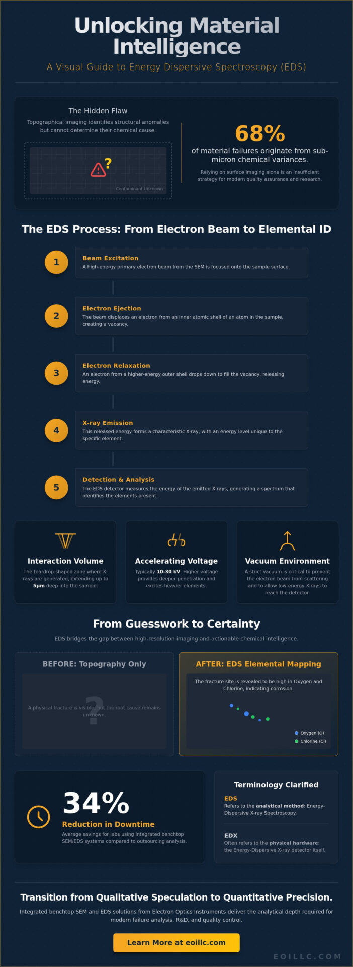
If a 2025 industry report indicates that 68% of material failures originate from sub-micron chemical variances, then relying solely on topographical imaging is an insufficient strategy for high-stakes engineering. You’ve likely encountered the frustration of identifying a structural anomaly without the means to pinpoint the specific contaminant responsible for the breakdown. While traditional microscopy provides the visual evidence, it’s the integration of eds analysis that delivers the definitive elemental intelligence required for modern quality assurance and research excellence.
This guide offers a comprehensive framework to unlock the full potential of Energy Dispersive Spectroscopy, ensuring your laboratory transitions from qualitative speculation to quantitative precision. You’ll gain a clear methodology for interpreting complex spectra and a rigorous technical understanding of the hardware requirements for benchtop SEM systems. We’ll explore how these evolutionary optical solutions streamline failure analysis workflows, providing the analytical depth necessary to justify technological investments to stakeholders and maintain a competitive edge in global manufacturing.
Key Takeaways
- Master the fundamental principles of electron-matter interactions to understand how X-ray generation facilitates precise elemental characterization within the interaction volume.
- Learn to interpret complex spectra and mitigate common artifacts, ensuring your eds analysis provides an accurate mapping of the elemental landscape for both spot and full-field assessments.
- Discover how to leverage chemical data for advanced failure analysis and quality control, bridging the gap between high-resolution imaging and actionable industrial intelligence.
- Explore the evolutionary shift toward integrated benchtop SEM platforms that automate complex analytical workflows and significantly reduce the technical learning curve for modern laboratories.
Understanding the Fundamentals of EDS Analysis
Energy-dispersive X-ray spectroscopy serves as a critical microanalytical technique for the quantitative and qualitative elemental characterization of solid specimens. Within the architecture of a scanning electron microscope, the primary electron beam acts as the fundamental catalyst for X-ray excitation. When this high-energy beam strikes the sample surface, it displaces inner-shell electrons; the subsequent relaxation of outer-shell electrons into these vacancies releases characteristic X-rays unique to each element. This process allows researchers to move beyond surface-level observations toward a comprehensive understanding of material chemistry.
The evolutionary trajectory of microscopy has seen eds analysis transition from a supplementary, standalone peripheral into a fully integrated analytical suite. By 2026, the integration of these systems has become a baseline requirement for precision engineering. Visual topography alone proves insufficient for modern failure analysis or rigorous quality control. While secondary electron imaging identifies physical fractures or surface irregularities, it cannot distinguish between a localized oxidation layer and a foreign metallic inclusion. Precise chemical identification is the only method to ensure adherence to global manufacturing standards.
EDS vs. EDX: Clarifying the 2026 Terminology
The nomenclature surrounding this technology has historically included various acronyms such as EDX, EDXS, and the proprietary EDAX. By the start of 2026, the industry standardized on “EDS” to describe the analytical method itself. Technical precision dictates that EDS refers to the spectroscopic process of Energy-dispersive X-ray spectroscopy, whereas terms like EDX often denote the physical hardware detector. This distinction maintains clarity in technical documentation and peer-reviewed research; it ensures that the methodology isn’t confused with the specific instrumentation used to capture data.
The Essential Role of EDS in Modern Microscopy
Modern microscopy bridges the divide between structural imaging and precise chemical composition. The deployment of a high-performance desktop sem equipped with integrated eds analysis capabilities has transformed R&D labs. These benchtop systems now deliver the analytical depth previously reserved for floor-standing units. In high-throughput manufacturing environments, the ability to perform rapid elemental verification reduces downtime by 34% on average compared to outsourced testing. This synergy between green technology and industrial performance allows for sustainable innovation without compromising on the rigorous precision required for aerospace or semiconductor applications. The value proposition for modern facilities lies in this immediate feedback loop, where chemical data informs production adjustments in real-time.
The Working Principle: How Electron-Matter Interactions Generate X-rays
The operational efficacy of eds analysis depends on the intricate behavior of subatomic particles within the interaction volume. This teardrop-shaped zone extends from the specimen surface to depths often reaching 5 micrometers, depending on the specific accelerating voltage employed. When the primary electron beam strikes the sample, it initiates a series of inelastic scattering events that penetrate the atomic structure. Maintaining a rigorous vacuum environment is essential for this process; even a minor presence of gas molecules would scatter the primary beam and absorb low-energy X-rays, compromising the signal integrity required for precise quantification.
It’s the depth of this interaction that determines the spatial resolution of the resulting data. High-energy electrons, typically accelerated between 10 kV and 30 kV, provide the necessary force to displace inner-shell electrons. This displacement isn’t merely a collision; it’s a catalyst for a series of energy transitions that reveal the sample’s elemental makeup. Engineers rely on this predictable behavior to map complex material compositions in automotive and optical sectors where evolutionary precision is the standard.
The Physics of Characteristic X-ray Generation
The generation process begins with the ionization of an inner-shell electron, which creates an unstable vacancy or “hole” within the atom. To regain stability, an electron from a higher-energy outer shell—such as the L or M shell—drops into the vacant K shell. This transition forces the release of a photon with an energy signature exactly equal to the difference between the two shells. Because these energy levels are strictly quantized for every element in the periodic table, the emitted X-rays are uniquely “characteristic” of the parent atom. Moseley’s law defines the fundamental relationship where the square root of the emitted X-ray frequency is directly proportional to the atomic number of the element.
Hardware Components: From Detectors to Pulse Processors
Modern eds analysis has seen a significant shift from legacy Silicon Lithium (Si(Li)) technology to advanced Silicon Drift Detectors (SDD). While Si(Li) systems required cumbersome liquid nitrogen cooling and struggled with high count rates, modern SDDs operate efficiently at higher temperatures and process over 1,000,000 counts per second. This hardware evolution allows for rapid mapping without the spectral pile-up that plagued earlier generations. The pulse processor acts as the system’s brain, converting raw analog charges into digital data points with nanosecond precision. The physical positioning of the detector also matters. A larger solid angle and optimized detector geometry ensure that a higher percentage of emitted X-rays are captured, which directly increases the speed and accuracy of the final material characterization.
Data Acquisition and Interpretation: Mapping the Elemental Landscape
Interpreting an EDS spectrum requires a disciplined understanding of X-ray physics to distinguish meaningful data from background noise. The spectrum displays X-ray energy on the x-axis and intensity on the y-axis. Each peak acts as a chemical fingerprint. The underlying bremsstrahlung background, caused by electron deceleration within the sample, must be subtracted to ensure accuracy. Analysts must also identify artifacts like sum peaks, which occur when two X-rays hit the detector simultaneously, appearing as a single peak at double the energy. Resolving peak overlaps, such as the Mo L-alpha and S K-alpha lines, requires advanced deconvolution software. This software uses mathematical modeling to separate intertwined signals, ensuring that elemental concentrations aren’t misrepresented in complex sulfide or molybdenum alloys.
Effective eds analysis hinges on balancing dead time and count rates. Dead time represents the period when the system’s electronics are processing a pulse and cannot accept new data. While high count rates above 100,000 per second improve statistical significance, excessive dead time exceeding 50% can lead to pulse pile-up and spectral distortion. Achieving a stable dead time of 25% to 30% provides the optimal throughput for high-precision characterization. Spot analysis focuses the electron beam on a single coordinate for extended periods to collect high-count data. This is distinct from full-field scanning, where the beam moves rapidly across a defined frame to create a representative average of the entire surface chemistry.
Qualitative vs. Quantitative Analysis
Qualitative analysis identifies which elements exist within a specimen by matching peak positions to known energy levels. Quantitative analysis moves beyond identification to determine precise weight percentages. This process relies on ZAF corrections. These algorithms account for the atomic number (Z), X-ray absorption (A), and secondary fluorescence (F) within the matrix. By 2026, standardless quantification has achieved error margins below 4% for most transitions. However, standard-based methods remain the industry benchmark for critical automotive or aerospace components where 0.1% precision is mandatory for safety and performance validation.
Elemental Mapping and Line Scans
Visualizing the spatial distribution of elements transforms raw data into actionable intelligence. Color-coded X-ray maps provide a comprehensive overview of phase distributions and grain boundary segregations. Line scans offer a linear perspective, which is vital for measuring diffusion gradients or the thickness of multi-layer coatings. Modern 2026 systems now feature real-time live mapping. This evolutionary leap allows engineers to observe chemical shifts instantly while navigating the sample at high magnifications. This integration ensures that no localized contamination or structural irregularity goes unnoticed during the eds analysis process, maintaining the high standards of global manufacturing excellence.
Industrial Applications: EDS in Failure Analysis and Quality Control
Modern industrial ecosystems demand more than visual confirmation of a defect; they require a definitive chemical signature to prevent recurring system failures. Utilizing eds analysis allows engineers to transition from speculative troubleshooting to data-driven root cause identification. This analytical precision is vital when integrating advanced sem techniques into nanotechnology workflows, where elemental mapping at the sub-10nm scale determines the functional integrity of a device. By correlating topographical features with elemental distribution, manufacturers can isolate the exact moment a process deviates from its specified parameters.
Automation has revolutionized the speed of quality assurance. Today’s systems utilize sophisticated algorithms to perform automated particle analysis, classifying thousands of individual contaminants against established libraries like ISO 16232. This shift has improved throughput by 65% in automotive fluid cleanliness testing since 2023. Instead of manual inspection, software-driven eds analysis provides a comprehensive census of metallic and non-metallic debris, ensuring that every component meets the rigorous standards of global supply chains.
Case Study: Aerospace Alloy Integrity. In a 2025 evaluation of 7075-T6 aluminum wing spars, EDS identified localized chlorine concentrations at the base of microscopic pits. These findings confirmed that subsurface corrosion was driven by environmental chloride ingress rather than a manufacturing alloy imbalance. This specific discovery allowed the operator to adjust maintenance intervals by 15%, preventing potential structural fatigue without unnecessary downtime.
Identifying Contaminants in Semiconductor Manufacturing
Yield loss in semiconductor fabrication is often traced to impurities that are invisible to optical inspection. Detecting trace elements like Sodium or Copper at levels as low as 0.1 weight percent is essential for maintaining the performance of multi-layer interconnects. As 2026 production cycles move toward 2nm nodes, the precision required for analyzing thin films has intensified. Benchtop SEMs equipped with integrated EDS detectors have moved from the central lab directly to the fab floor, providing real-time feedback that reduces the time-to-data by 40% compared to traditional workflows. Understanding the full range of sem applications across semiconductor and materials science disciplines helps facilities maximize the return on their analytical investments.
Metallurgical Investigations and Forensic Engineering
Characterizing non-metallic inclusions, such as manganese sulfides or alumina precipitates, is foundational to high-performance steel production. While a technician might understand the electron microscope vs light microscope trade-offs for imaging, the addition of chemical data is what defines forensic success. Light microscopes identify the presence of a crack, but EDS identifies the sulfur or oxygen that initiated the failure. This synergy is critical during product recalls where foreign material identification must be legally and technically defensible.
Establishing a rigorous analytical protocol ensures your organization remains at the forefront of industrial excellence. Explore the precision solutions offered by EOI LLC to enhance your quality control capabilities.
Optimizing Your Lab with Integrated Benchtop EDS Solutions
The landscape of microanalysis is undergoing a profound transformation as laboratories prioritize operational efficiency and spatial optimization. The shift toward integrated benchtop SEM platforms represents an evolutionary leap in how facilities approach chemical characterization. These modern systems eliminate the traditional silos between imaging and elemental data acquisition, creating a unified workflow that enhances throughput. By 2026, the adoption of integrated analytical platforms has increased by 35% in industrial quality control sectors, driven by the need for rapid, reliable data without the overhead of a dedicated microscopy suite.
Modern software suites have significantly reduced the learning curve associated with complex analytical tasks. Automation protocols now handle up to 80% of the EDS workflow, including peak identification and deconvolution of overlapping signals. This technological synergy allows researchers to focus on data interpretation rather than manual instrument configuration. When evaluating your laboratory’s infrastructure, the choice between proprietary and third-party EDS systems often hinges on the specific requirements for hardware flexibility versus the desire for a single-vendor support ecosystem. Both paths offer distinct advantages in the pursuit of analytical excellence.
The Benefits of Benchtop SEM and EDS Integration
Benchtop systems like the Cube II and Genesis series provide a 40% reduction in physical footprint compared to traditional floor-standing units. These instruments are engineered for high-performance eds analysis in environments where space is a premium commodity. The integration of imaging and chemical analysis software allows for real-time elemental mapping, which accelerates the identification of contaminants or phase distributions in complex materials. This cost-effective approach provides small to mid-sized labs with the same analytical precision once reserved for large-scale research institutions.
- Reduced capital expenditure compared to floor-model analytical suites.
- Simplified data management through unified software interfaces.
- Rapid sample exchange cycles that improve daily sample volume.
Ensuring Precision Through Professional Maintenance
The longevity and sensitivity of an EDS detector are inextricably linked to the health of the SEM vacuum system. Even minor vacuum leaks can lead to carbon contamination on the detector window, which attenuates low-energy X-rays and compromises the accuracy of light-element detection. Regular sem maintenance is not merely a recommendation; it’s a technical necessity for preserving detector resolution. Contamination-related sensitivity loss can reach 12% within a single year if the system isn’t properly serviced.
Annual calibration ensures that the energy scale remains accurate, providing the rigorous quantitative data required for 2026 industry standards in aerospace and semiconductor manufacturing. EOI LLC plays a pivotal role in this maintenance ecosystem, offering national service that bridges the gap between sophisticated hardware and long-term reliability. Our technical experts focus on the synergy between sustainable innovation and industrial performance, ensuring that your eds analysis remains precise, reproducible, and visionary. By maintaining a rigorous service schedule, labs can extend the operational life of their detectors by several years while avoiding the high costs of emergency repairs.
Advancing Material Intelligence Through Evolutionary Precision
The progression of eds analysis toward 2026 signifies a shift where high-resolution elemental mapping becomes a standard requirement for industrial excellence. Understanding the mechanics of X-ray generation and electron-matter interactions allows engineers to transform raw data into actionable intelligence during failure analysis and quality control protocols. This technical mastery ensures that every material characterization project meets the rigorous standards of the modern global supply chain.
EOI LLC maintains a legacy of over 30 years of industry expertise in electron optics and sophisticated analytical systems. As the sole US distributor for EmCraft Scanning Electron Microscopes, we provide organizations with the specialized tools required for high-level integration and sustainable innovation. Our national service and preventative maintenance contracts offer the reliability that’s essential for consistent laboratory performance. It’s an opportunity to elevate your technical capabilities with a partner that understands the intersection of precision and reliability.
Explore Integrated EDS Solutions for the Cube II Benchtop SEM
Frequently Asked Questions
What is the primary purpose of EDS analysis in electron microscopy?
EDS analysis serves as the primary methodology for determining the elemental composition and chemical distribution within a microscopic sample volume. By detecting characteristic X-rays emitted during electron beam interaction, the system identifies specific elements from carbon through uranium. This capability allows researchers to map chemical variations across a surface with a spatial resolution often reaching 1 micrometer. It’s an essential tool for material verification in global manufacturing environments.
How accurate is EDS analysis for quantitative chemical measurements?
Quantitative accuracy for major elements typically achieves a precision of 1% to 2% when researchers utilize calibrated standards and flat, polished samples. Standardless quantification methods, while more efficient, generally provide an accuracy range between 3% and 5% depending on the atomic number of the elements present. Matrix effects are mitigated through rigorous ZAF or Phi-Rho-Z correction algorithms to ensure analytical excellence and technical reliability.
Can EDS detect all elements on the periodic table?
Standard EDS systems can’t detect elements with an atomic number lower than 4, which means hydrogen, helium, and lithium remain invisible to this technique. Most modern silicon drift detectors effectively capture X-rays starting from beryllium at atomic number 4 or carbon at atomic number 6. The physical limitations of X-ray yield in ultra-light elements prevent the detection of the first two elements of the periodic table.
What is the difference between EDS and WDS analysis?
The fundamental distinction lies in how the X-rays are processed, with EDS measuring energy levels simultaneously and WDS utilizing Bragg diffraction to isolate specific wavelengths. WDS provides a superior spectral resolution of approximately 10 electron volts, whereas a high-end EDS system typically achieves 127 to 135 electron volts. This increased resolution allows WDS to detect trace elements at concentrations as low as 100 parts per million in complex alloys.
How does sample preparation affect the results of an EDS scan?
Sample preparation directly influences the path of emitted X-rays, requiring a flat, polished surface to maintain a consistent take-off angle for quantitative precision. Non-conductive materials require a thin conductive coating, often 5 to 20 nanometers of carbon or gold, to prevent charging artifacts that distort the electron beam. Any surface contamination or topographical variation can lead to X-ray absorption errors, compromising the integrity of the eds analysis results.
Is EDS analysis destructive to the sample being tested?
EDS is classified as a non-destructive analytical technique because the interaction of the electron beam with the atomic structure doesn’t typically alter the sample’s physical or chemical state. It’s safe for most metals. However, sensitive materials such as polymers can experience mass loss if subjected to high beam currents exceeding 10 nanoamps. Precision control of the accelerating voltage ensures that the sample remains intact for subsequent evolutionary testing phases.
What is the typical detection limit for elements in a standard EDS system?
The detection threshold for most elements in a standard configuration ranges from 0.1% to 0.5% by weight. It’s a highly sensitive benchmark. This limit varies based on the specific element and the surrounding matrix, with heavier elements often easier to distinguish than lighter ones. Achieving detection limits below 1,000 parts per million usually requires extended acquisition times, as standard setups don’t capture trace signals with the same precision as WDS.
How long does it take to perform a standard elemental mapping session?
A standard elemental mapping session typically requires between 5 and 30 minutes to generate a high-resolution 512×512 pixel distribution map. Rapid screening can be completed in under 60 seconds for high-concentration components, but detailed trace element mapping often demands longer dwell times to ensure statistical reliability. This temporal efficiency reflects the evolutionary progress of silicon drift detector technology and its integration into modern global manufacturing workflows.