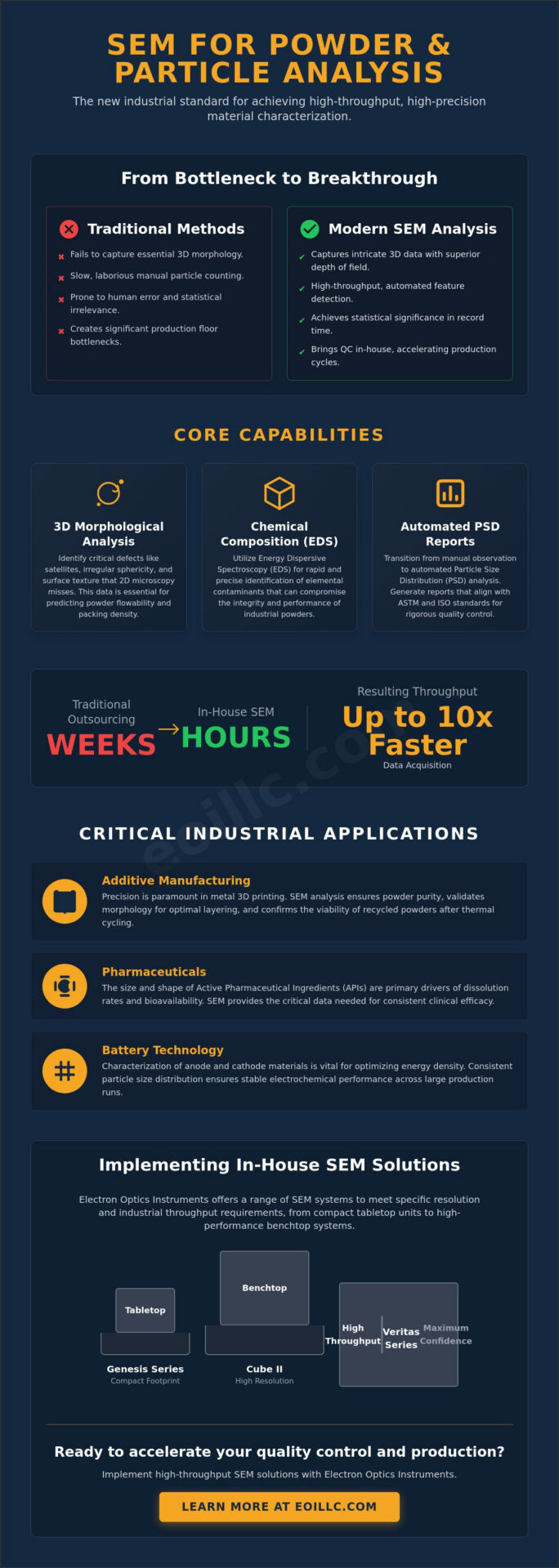
In the rigorous landscape of 2026 industrial manufacturing, the primary bottleneck in material characterization is no longer the resolution of the image, but the velocity of data acquisition. While traditional methods often stall at the intersection of precision and throughput, utilizing sem for powder and particle analysis has emerged as the definitive standard for achieving statistical significance in record time. Industry professionals recognize that manual particle counting is a laborious process prone to human error, while standard optical microscopes frequently fail to provide the necessary depth of field for complex 3D powder morphology. This technical guide demonstrates how modern benchtop and tabletop SEM systems, such as the Cube II or the Veritas Series, bridge the gap between high-end research capabilities and the practical demands of the production floor.
You’ll discover how advanced hardware facilitates high-throughput, automated characterization of powder morphology and chemical composition for critical industrial applications. We’ll examine the integration of Energy Dispersive Spectroscopy (EDS) for rapid contaminant identification and the transition toward automated Particle Size Distribution (PSD) reports that align with current ASTM and ISO standards. By bringing these advanced characterization workflows in-house, organizations can achieve results up to ten times faster than through traditional outsourcing models, ensuring that meticulous quality control keeps pace with the grounded realities of international production and logistical excellence.
Key Takeaways
- Understand the critical limitations of 2D optical microscopy and how electron beam topography captures essential 3D morphological data such as particle sphericity and satellite formations.
- Learn how to utilize Energy Dispersive Spectroscopy (EDS) for the precise chemical identification of elemental contaminants that compromise the integrity of industrial powders.
- Evaluate the technical feasibility of implementing sem for powder and particle analysis within a standard lab footprint using high-resolution benchtop systems like the Cube II.
- Master the transition from manual observation to automated feature detection by establishing rigorous threshold parameters for accurate particle-to-background separation.
- Identify the optimal hardware configuration, ranging from the Genesis Tabletop to the Veritas Series, based on specific sub-micron resolution and industrial throughput requirements.
The Critical Role of SEM in Modern Powder Characterisation
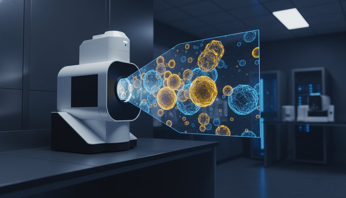
The Scanning Electron Microscope (SEM) functions by scanning a specimen with a focused beam of electrons, which interact with atoms in the sample to produce signals containing exhaustive data about surface topography and composition. Unlike traditional light-based methods, utilizing sem for powder and particle analysis offers a superior depth of field that captures the intricate 3D structures of individual grains. This capability is essential for modern manufacturing. Standard 2D optical microscopy often fails to identify critical defects such as satellites or irregular sphericity. These minute morphological flaws directly impede the flowability and packing density of powders, which ultimately compromises the structural integrity of the final manufactured component. Precision dictates performance, and it’s this level of detail that separates high-end industrial production from standard manufacturing.
The current shift toward benchtop SEM systems, such as the Cube II or Genesis Tabletop models, enables organizations to implement real-time quality control directly within production environments. This transition minimizes the reliance on external facilities, reducing lead times from weeks to hours. By maintaining high-resolution imaging capabilities in a compact footprint, these systems ensure that material specifications are met with unwavering accuracy. The deployment of electron optics facilitates a level of meticulousness that traditional light-based systems cannot replicate, providing a visionary path for companies focused on technical excellence.
Key Industries Dependent on Particle Analysis
- Additive Manufacturing: Precision is paramount in metal 3D printing. SEM analysis ensures powder purity and validates whether recycled powders remain viable for reuse after multiple thermal cycles.
- Pharmaceuticals: Scientists monitor the size and shape of Active Pharmaceutical Ingredients (APIs). These factors are the primary drivers of dissolution rates and bioavailability in clinical applications.
- Battery Technology: The characterisation of anode and cathode materials is vital for optimizing energy density. Consistent particle size distribution ensures stable electrochemical performance across large-scale production runs.
Beyond Size: Understanding Morphology and Surface Texture
The utility of sem for powder and particle analysis extends far beyond simple diameter measurements. Surface texture and morphology dictate how particles interact under pressure and heat. Identifying ‘satellites’, which are smaller particles fused to larger ones, is critical because they increase friction and hinder powder flow in automated delivery systems. Surface porosity analysis also plays a role in determining chemical reactivity; higher porosity can lead to unexpected oxidation or accelerated reactions. Detecting these issues, along with agglomeration trends, allows engineers to adjust process parameters before defects manifest in the final product. Meticulous characterization via the Veritas Series or Veritas HR SEM provides the data-driven confidence required for high-stakes industrial applications where reliability is the only acceptable standard.
Technical Mechanisms: How SEM Analyses Particle Composition
The efficacy of sem for powder and particle analysis resides in the intricate interaction between the primary electron beam and the specimen surface. When the beam strikes the powder grains, it generates Secondary Electrons (SE) and Backscattered Electrons (BSE), each providing distinct datasets for the operator. SE imaging is primarily utilized for topographic mapping; its high depth of field allows for the clear visualization of spherical particles, ensuring that every satellite and surface irregularity is in sharp focus across the entire curvature of the grain. This level of resolution is indispensable for maintaining the meticulous standards required in specialized industrial sectors where precision dictates the viability of the final product.
Operational success also depends on the management of vacuum environments within the chamber. While metallic powders are inherently conductive and facilitate easy imaging under high vacuum, non-conductive materials like certain polymers or pharmaceutical APIs require specialized handling to prevent charging. Systems like the Veritas Series or the Cube II are engineered to handle these variations, ensuring that the integrity of the data remains uncompromised regardless of the material’s electrical properties. For those seeking to integrate these capabilities into their own facilities, exploring the range of advanced SEM hardware is a logical next step toward technical self-sufficiency and logistical excellence.
Elemental Mapping with Integrated EDS
The deployment of Energy Dispersive Spectroscopy (EDS) Systems transforms the SEM from a mere imaging tool into a powerful chemical analyzer. As the electron beam displaces inner-shell electrons, the resulting X-ray emissions act as unique atomic signatures. This process allows for the creation of chemical heat maps, enabling engineers to distinguish between the core material and surface oxidation or foreign impurities. In heterogeneous powder mixtures, this capability ensures that the precise atomic makeup of individual particles is documented, providing a level of accuracy that is foundational to modern quality assurance protocols.
Backscattered Electron (BSE) Imaging for Phase Contrast
BSE imaging leverages Z-contrast, where elements with higher atomic numbers appear brighter due to their higher rate of electron reflection. This mechanism is particularly effective for high-throughput screening, as it allows for the immediate identification of heavy-metal contaminants within light-element powders. In complex alloys, BSE detectors assist in identifying multi-phase particles and inclusions that might otherwise remain undetected. Optimizing these detectors within a system like the Veritas HR SEM enhances the speed of data acquisition, pushing the boundaries of what’s possible in large-scale industrial characterization.
Benchtop vs. Traditional SEM for Particle Analysis
Selecting the appropriate hardware for sem for powder and particle analysis requires a rigorous assessment of resolution requirements against the logistical realities of facility integration. While high-end Veritas FE SEM systems provide the sub-nanometer resolution essential for advanced nanomaterial research, many industrial applications find that the performance of a Cube II Benchtop SEM is more than sufficient for characterizing micro-scale powders. The primary differentiator often resides in the infrastructure; traditional floor-model SEMs necessitate dedicated microscopy suites equipped with specialized vibration isolation and electromagnetic shielding. Conversely, modern benchtop units function effectively on a standard laboratory bench, facilitating decentralized testing closer to the production line where immediate data is most valuable.
Total Cost of Ownership (TCO) in 2026 encompasses far more than the initial capital expenditure. Traditional systems incur substantial operational costs, including high power consumption and the requirement for specialized microscopists. Benchtop systems utilize automated software that simplifies stage control and feature detection, which allows staff with standard laboratory training to generate high-quality data. This democratization of electron microscopy enhances operational throughput, as it removes the bottleneck of waiting for a centralized facility’s schedule. It’s a visionary approach that prioritizes reliability and rapid iteration in high-stakes manufacturing environments.
Performance Benchmarks for Powder Analysis
For particles ranging from 100nm to 100µm, benchtop systems offer data quality that rivals their larger counterparts. When analyzing non-conductive powders, the capability to operate in low-vacuum mode reduces the necessity for sputter coating, thereby preserving the original surface morphology for more accurate characterization. You can explore this transition in our detailed analysis of Desktop SEM: The Evolutionary Shift to High-Performance Benchtop Microscopy in 2026. Understanding these resolution thresholds is vital for ensuring that the chosen system aligns with the specific physical properties of the material being studied.
Operational Efficiency and Lab Integration
Reliability remains a cornerstone of industrial excellence, and maintaining system integrity is paramount for consistent results. While benchtop units like the Genesis Tabletop SEM are designed for ease of use, they still require methodical care to ensure long-term accuracy. Implementing a consistent schedule of Preventative Maintenance Visits ensures that apertures and SEM filaments remain in peak condition, preventing unexpected downtime. For a comprehensive breakdown of the investment levels associated with these systems, refer to How Much Does an Electron Microscope Cost? A Comprehensive 2026 Price Guide.
Optimising Workflow: Automated Particle Analysis
Manual characterisation has historically been the primary constraint in material science workflows, often requiring hours of meticulous observation to reach statistical relevance. The integration of automated feature detection within sem for powder and particle analysis has effectively dismantled this barrier, enabling the analysis of over 1,000 particles in mere minutes. Modern systems, such as the Phenom ParticleX AM, demonstrate this efficiency by processing up to 49 samples simultaneously, delivering comprehensive results within a single day. This rapid data acquisition is vital for industries where production cycles are measured in hours, not weeks. Every grain is accounted for with a level of precision that manual counting simply cannot replicate.
Efficiency is refined through the seamless export of characterisation data into Laboratory Information Management Systems (LIMS). By automating the generation of Particle Size Distribution (PSD) reports, organizations eliminate the risk of human transcription errors. This structured approach ensures that every morphological metric, from aspect ratio to circularity, is documented with meticulousness. For those looking to optimize their internal workflows, investing in high-throughput SEM hardware ensures that your quality control processes remain as rigorous as your engineering standards.
Five Steps to Automated PSD Reporting
- Step 1: Sample Dispersion. Particles are dispersed on carbon tape or filtered onto membranes to ensure individual grains are distinct and measurable without overlapping.
- Step 2: Defining ROI. Operators define the Region of Interest and select magnification levels that balance high resolution with the necessary field of view for statistical significance.
- Step 3: Binary Segmentation. Setting precise grey-scale thresholds allows the software to accurately separate particles from the background substrate for automated detection.
- Step 4: EDS Acquisition. Real-time chemical analysis identifies elemental contaminants while the beam maps the physical morphology of the powder.
- Step 5: Data Synthesis. The system compiles all measurements into a standardised report, reaching analysis rates of up to 10,000 particles per hour for immediate stakeholder review.
Ensuring Data Integrity and Repeatability
Standardising magnification and beam settings across different operators is fundamental for maintaining longitudinal data accuracy. Even minor fluctuations in accelerating voltage can impact the perceived size of sub-micron particles, making stage calibration a critical prerequisite for large-area automated mapping. You’ll find a detailed breakdown of these technical requirements in SEM Operation: The Professional Guide to Scanning Electron Microscopy in 2026. Consistency is the anchor of industrial reliability, ensuring that every batch meets the visionary standards of high-end production.
Implementing SEM Solutions with Electron Optics Instruments
Achieving technical excellence in characterization requires a synergy between sophisticated hardware and rigorous operational support. While the preceding chapters detailed the mechanisms of sem for powder and particle analysis, the practical implementation of these workflows depends on selecting a platform that balances resolution with industrial reliability. Electron Optics Instruments, LLC provides this foundation through the Cube II Benchtop SEM, a system specifically engineered to bridge the gap between research-grade imaging and the high-throughput demands of the production floor. By integrating customized EDS Systems, organizations can tailor their elemental analysis to the specific chemical profiles of their proprietary powders, ensuring that every contaminant is identified with unwavering precision.
Operational success isn’t solely defined by the initial hardware acquisition; it’s sustained through the meticulousness of ongoing technical support. Electron Optics Instruments, LLC facilitates this through comprehensive service contracts and on-site technical training programs that empower internal teams to master automated analysis. This strategic integration of expert knowledge and advanced hardware ensures that the characterization process remains a pillar of stability within the manufacturing cycle. It’s a visionary approach that prioritizes long-endurance accuracy and logistical excellence over short-term expediency. For those ready to implement these high-throughput capabilities, exploring our range of specialized SEM solutions is the definitive next step.
Why the Cube II is the Benchmark for Powder Labs
The Cube II Benchtop SEM delivers superior resolution within a compact frame, making it the ideal solution for sub-micron particle detection where laboratory space is at a premium. Its robust vacuum systems are designed to handle diverse powder types, from metallic additives to sensitive pharmaceutical compounds, without compromising data integrity. The user-friendly interface is specifically optimized for rapid QA/QC workflows, allowing for the seamless transition from sample loading to the generation of actionable data. This combination of performance and accessibility ensures that high-resolution imaging remains a grounded reality for modern industrial partners.
Expert Support and Maintenance for Long-Term Accuracy
Reliability in particle characterization is directly linked to the health of the electron optics system. Small deviations in beam alignment or filament wear can introduce subtle inaccuracies that compromise the statistical significance of your data. Leveraging the three decades of expertise at Electron Optics Instruments, LLC, our Preventative Maintenance Visits are designed to preempt these issues before they impact production schedules. Maintaining this level of precision is a fundamental requirement for adhering to international standards. For a deeper exploration of these protocols, consult The Definitive Guide to SEM Maintenance: Maximizing Precision and Longevity in 2026. Consistent care ensures that your sem for powder and particle analysis remains a reliable anchor for your quality assurance strategy.
Advancing Industrial Excellence through Automated Characterisation
The transition toward high-throughput, automated characterisation represents a fundamental shift in how organisations approach material integrity. By integrating the advanced hardware discussed throughout this guide, facilities can achieve statistical significance in minutes rather than days. This technical evolution ensures that the implementation of sem for powder and particle analysis remains a cornerstone of quality assurance, effectively bridging the gap between sophisticated research and the practical demands of large-scale production.
As the sole US distributor for EmCraft Scanning Electron Microscopes, Electron Optics Instruments, LLC leverages over 30 years of industry-leading expertise to support your characterisation goals. We provide comprehensive service contracts for all major SEM brands, ensuring that your production lab maintains peak data precision without unexpected downtime. Our technical team is prepared to assist you in navigating the complexities of sub-micron analysis and automated reporting workflows. Request a Technical Consultation for Your Powder Analysis Needs today to ensure your facility remains at the forefront of technical innovation and logistical excellence.
Frequently Asked Questions
How does SEM compare to laser diffraction for particle size analysis?
Laser diffraction calculates equivalent spherical diameters, often overlooking the high-aspect ratio grains or surface satellites identified in sem for powder and particle analysis. While diffraction provides rapid volume-weighted distributions, SEM delivers the visual evidence required to troubleshoot flowability issues in metal powders or pharmaceutical blends. This direct observation is critical for verifying that the physical realities of the material align with theoretical scattering models, providing a more meticulous understanding of grain morphology.
Can SEM detect contaminants within a powder sample?
SEM identifies contaminants by leveraging the contrast between different atomic numbers in Backscattered Electron (BSE) mode. Heavy-metal inclusions appear as distinct, bright anomalies against lighter organic or ceramic backgrounds, providing an immediate visual flag for impurities. When coupled with Energy Dispersive Spectroscopy (EDS), the system identifies the specific elemental composition of these foreign particles, enabling manufacturers to trace contamination back to specific stages of the production process with technical authority.
Is sample coating always necessary for powder analysis in an SEM?
Conductive coating is no longer a strict requirement for most industrial powders due to the development of variable pressure and low-vacuum technologies. These modes introduce a small amount of gas into the chamber to neutralize the buildup of surface electrons on non-conductive specimens like polymers or active ingredients. This advancement preserves the original surface texture and porosity, which is essential for accurate reactivity studies where a metallic coating might obscure critical morphological features.
How many particles should be analysed for a statistically significant result?
A statistically significant result typically requires characterizing between 500 and 1,000 particles, though high-stakes additive manufacturing often demands larger datasets for confidence. Utilizing sem for powder and particle analysis with automated software facilitates the measurement of over 10,000 particles per hour, far exceeding manual capabilities. This volume of data ensures that the resulting Particle Size Distribution (PSD) curve accurately represents the heterogeneity within large industrial batches, maintaining a visionary standard for quality control.
Can a benchtop SEM handle non-conductive pharmaceutical powders?
Benchtop systems like the Cube II are specifically engineered to handle non-conductive pharmaceutical powders by utilizing specialized low-voltage imaging and variable pressure environments. These features prevent the charging artifacts that typically degrade image quality on organic materials, allowing for the clear visualization of API crystals and excipient distributions. This capability ensures that pharmaceutical researchers can maintain rigorous quality standards without the need for complex sample preparation or large-scale floor models.
What is the typical throughput for automated SEM particle analysis?
Automated throughput for modern electron optics systems has reached a threshold where analyzing 10,000 particles per hour is now a standard operational benchmark. Some high-capacity systems can load up to 49 samples simultaneously, providing a comprehensive characterization report within a single workday. This rapid turnaround is vital for maintaining the momentum of international production lines, where waiting ten working days for outsourced results is no longer a viable logistical option in a high-speed market.
How does integrated EDS improve powder characterisation?
Integrated EDS improves characterization by providing a chemical overlay to the physical morphology, effectively creating a multi-dimensional map of the specimen. This allows operators to distinguish between particles that appear physically identical but possess different elemental signatures, such as various metal oxides or alloy phases. By correlating chemical composition with size and shape, engineers gain a visionary understanding of how specific impurities impact the overall performance and reliability of the final manufactured product.
What are the maintenance requirements for an SEM used in high-volume powder testing?
High-volume powder testing requires a methodical maintenance strategy focused on the longevity of SEM filaments and the cleanliness of the final apertures. Frequent sample loading can introduce particulates into the column, necessitating periodic vacuum system checks and stage recalibration to ensure automated mapping remains precise. Maintaining a consistent service interval with Electron Optics Instruments, LLC ensures that your hardware continues to push the boundaries of accuracy while minimizing the risk of unplanned production downtime.