

Could the persistent reliance on a singular detection modality be the hidden catalyst for suboptimal data interpretation within your material characterization and failure analysis workflows? For industry professionals operating at the vanguard of materials science, the persistent difficulty of distinguishing between discrete phases in complex alloys or achieving necessary surface resolution on non-conductive samples remains a significant technical hurdle. You likely recognize that a superficial understanding of detector physics often results in ambiguous results that stall critical R&D milestones. Precision is non-negotiable. This technical analysis clarifies the sophisticated distinctions inherent in backscattered vs secondary electron imaging, providing the rigorous framework needed to optimize your laboratory’s analytical capabilities in 2026.
By mastering these nuanced electron interactions, you’ll gain the expertise to maximize the utility of advanced hardware like the Cube II benchtop SEM. We’ll explore the precise criteria for detector selection, the synergistic relationship between SE and BSE modes, and the methodological advancements that facilitate faster, more accurate failure analysis. This guide ensures your facility transitions from basic observation to comprehensive material intelligence, aligning your operations with the rigorous standards of a global market projected to reach a valuation of USD 8.86 billion by 2034.
Key Takeaways
- Understand how discrete electron-matter interactions define signal depth, ensuring you don’t misinterpret topographical data as compositional variations during high-resolution analysis.
- Leverage secondary electron imaging to achieve superior surface resolution and morphological clarity when analyzing complex topographical features or non-conductive materials.
- Implement a rigorous technical comparison of backscattered vs secondary electron imaging to accurately identify phase distributions and atomic number variations within multi-component industrial alloys.
- Determine the optimal imaging mode for specialized workflows, prioritizing SE for nanotechnology while utilizing BSE for precise compositional mapping and failure analysis.
- Maximize analytical throughput by integrating dual-detector arrays in high-performance benchtop systems like the Cube II to facilitate simultaneous topographical and chemical data acquisition.
Understanding the Fundamental Physics of Electron-Matter Interactions
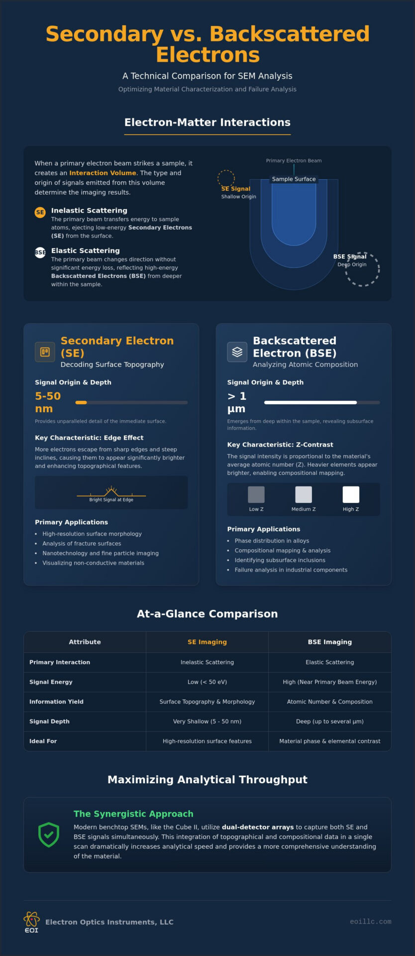
To achieve analytical excellence in modern microscopy, one must first master the intricate physics governing how a primary electron beam interacts with a specimen. As the beam strikes the sample, it triggers a cascade of events within a localized region known as the interaction volume. This volume’s dimensions and the resulting signal types are the foundation of any technical comparison regarding backscattered vs secondary electron imaging. The precision of your data depends entirely on your ability to distinguish between these discrete electron-matter interactions.
Secondary electrons (SE) are defined as low-energy particles, typically possessing less than 50 eV, that are ejected from the K-shell of sample atoms following inelastic collisions. Conversely, backscattered electrons (BSE) represent high-energy electrons that have undergone elastic scattering with the nucleus, effectively reflecting back out of the sample while retaining a significant portion of their original kinetic energy. The shape of the interaction volume, often resembling a teardrop or pear, is dictated by the beam’s accelerating voltage and the sample’s average atomic number. Understanding this spatial distribution is vital for researchers using a Scanning electron microscope to ensure the data captured aligns with the specific depth of interest.
The Mechanism of Elastic vs. Inelastic Scattering
Inelastic scattering occurs when the primary beam transfers energy to the sample’s electrons, a process that facilitates topographical sensitivity by generating SE signals. Elastic scattering, however, involves a change in direction without significant energy loss, producing deep-penetrating BSE signals that are sensitive to atomic mass. Adjusting the beam voltage (kV) allows operators to manipulate the size of the interaction volume, thereby refining the resolution or the depth of the analytical probe for complex material characterization.
Signal Origin and Depth of Information
The depth of information varies dramatically between these two modalities. SE signals originate almost exclusively from the top 5 to 50 nm of the surface, providing unparalleled detail on morphology. BSE signals emerge from much deeper within the specimen, sometimes reaching depths of several microns in lower-density materials. Maintaining a high-performance vacuum system is critical during this process, as gas molecules can scatter the beam and degrade the signal integrity required for precise backscattered vs secondary electron imaging. This depth-specific data is essential for identifying subsurface inclusions that surface-level SE scans might overlook.
Secondary Electron (SE) Imaging: Decoding Surface Topography and Morphology
Secondary electron imaging serves as the primary modality for visualizing surface morphology with exceptional fidelity. By capturing low-energy electrons emitted from the uppermost layers of a specimen, this technique provides high-resolution insights into grain boundaries, fracture surfaces, and delicate biological structures. The Everhart-Thornley (E-T) detector plays a pivotal role in this process; it utilizes a biased Faraday cage to attract these low-energy particles, even those not in a direct line of sight. This configuration is fundamental when evaluating backscattered vs secondary electron imaging, as SE detection is specifically optimized for surface-level detail rather than subsurface density variations.
One of the most technically significant features of SE imaging is the “Edge Effect.” Because secondary electrons are emitted from a shallow escape depth, sharp corners, ridges, and steep inclines allow more electrons to exit the sample surface compared to flat regions. This phenomenon results in these features appearing significantly brighter, providing the high contrast necessary to identify micro-cracks or fine textures that would otherwise remain obscured. It’s this specific sensitivity that makes SE imaging the standard for assessing the integrity of complex industrial components.
Topographical Contrast and Three-Dimensionality
The characteristic “3D” quality of SEM micrographs is a direct result of topographical shadowing. When the E-T detector is positioned to one side of the chamber, it creates a directional collection bias that mimics a light source, casting shadows across surface irregularities. Laboratory technicians don’t just rely on default settings; they often optimize the working distance (WD) to balance depth of field with resolution, ensuring that fatigue cracks and surface pitting are clearly defined during failure analysis. For organizations looking to integrate these high-level capabilities into their existing workflows, exploring the latest SEM advancements can provide a significant competitive edge in material characterization.
In-Lens vs. Chamber Detectors
Modern SEM systems often feature a choice between in-lens and chamber-mounted detectors to suit different analytical requirements. In-lens detectors are integrated within the objective lens, utilizing the magnetic field to capture SEs with extreme efficiency at very short working distances. This setup is superior for ultra-high resolution tasks where surface detail at the nanometer scale is paramount. Conversely, chamber detectors offer a broader field of view, making them better suited for large-scale topographical surveys. Managing charging effects on non-conductive samples is another critical consideration; lower accelerating voltages or specialized scan strategies are frequently employed to maintain image stability without sacrificing resolution.
Backscattered Electron (BSE) Imaging: Analyzing Atomic Composition and Phase Contrast
While secondary electrons define the physical boundaries of a specimen, backscattered electron (BSE) imaging provides the vital chemical context necessary for advanced material characterization. The primary mechanism behind BSE imaging is atomic number (Z) contrast. Atoms with higher atomic numbers possess larger, more positively charged nuclei, which results in a higher probability of elastic scattering events. Consequently, heavier elements like gold or tungsten appear significantly brighter in a micrograph than lighter elements such as carbon or aluminum. This direct relationship between signal intensity and material density allows researchers to distinguish between discrete phases in complex alloys or ceramic composites with remarkable clarity.
The high-energy nature of backscattered electrons also offers a distinct advantage when imaging samples with minor surface imperfections. Because these electrons originate from deeper within the interaction volume, they can effectively penetrate thin surface contaminants, such as light oxidation or residual carbon films, that might otherwise obscure topographical data in SE mode. When evaluating the technical trade-offs of backscattered vs secondary electron imaging, it becomes clear that BSE is the superior modality for identifying subsurface inclusions and heavy-metal contaminants that do not exhibit a distinct topographical signature.
Compositional vs. Topographical BSE Modes
Modern multi-quadrant BSE detectors enable a sophisticated level of control over signal acquisition. By summing the signals from all quadrants, operators achieve pure Z-contrast, where brightness correlates strictly with atomic mass. Conversely, subtracting signals from opposite quadrants creates a topographical BSE effect, often referred to as shadow mode. This technique is particularly effective for enhancing the surface features of high-density materials where traditional SE imaging might suffer from extreme charging or insufficient contrast, providing a versatile alternative for metallurgical examinations.
Synergy with Energy Dispersive Spectroscopy (EDS)
BSE imaging serves as the essential precursor to EDS analysis by providing a visual map of chemical heterogeneity. By identifying regions of interest (ROIs) based on grayscale variations, technicians can strategically target point analyses or line scans for precise chemical quantification. This methodological synergy significantly accelerates failure analysis cycles. It allows for the immediate correlation of image brightness with specific chemical species, ensuring that EDS data acquisition is both targeted and efficient, rather than a randomized survey of the sample surface. In the context of backscattered vs secondary electron imaging, this compositional sensitivity is what transforms a simple image into a data-rich analytical tool.
Strategic Comparison: Selecting the Optimal Imaging Mode for Specific Industrial Applications
Selecting the correct detection modality is not merely a technical preference; it’s a strategic decision that dictates the accuracy of your failure analysis and R&D outcomes. A robust understanding of backscattered vs secondary electron imaging allows laboratory managers to allocate resources effectively while minimizing the risk of data misinterpretation. While secondary electron imaging remains the standard for nanotechnology and biological structures due to its extreme surface sensitivity, backscattered electron imaging has become indispensable in metallurgy and mineralogy. The choice shouldn’t be viewed as a binary one. Modern high-performance systems enable simultaneous acquisition, providing a holistic data set that merges topographical detail with chemical context.
Strategic prioritization depends on the specific information required from the specimen. If the objective is to evaluate surface coatings or the fine morphology of nanostructures, SE imaging is the superior choice. However, when the focus shifts to identifying heavy-metal inclusions or mapping phase distributions in complex alloys, BSE imaging provides the necessary Z-contrast. Contrary to legacy assumptions that SE always offers higher resolution, modern semiconductor-grade detectors allow for compositional mapping at the nanoscale, bridging the gap between these two modalities. To enhance your laboratory’s diagnostic precision, consider exploring our range of SEM solutions tailored for rigorous industrial excellence.
Application Spotlight: Semiconductor Failure Analysis
In the semiconductor sector, the integration of both modes is critical for root cause determination. SE imaging is utilized to identify physical defects such as wire bond fractures or resist residue, where surface morphology is the primary concern. Conversely, BSE imaging is essential for detecting material diffusion and dielectric layer inconsistencies that occur beneath the immediate surface. Mastering sem operation ensures that technicians can toggle between these modes to distinguish between a physical crack and a chemical variation, ensuring a comprehensive understanding of device failure.
Application Spotlight: Metallurgical Phase Characterization
Metallurgical workflows benefit significantly from the contrast provided by BSE detectors. While SE imaging is effective for visualizing grain boundaries and surface fractures, BSE is superior for identifying second-phase precipitates and inclusions. For instance, detecting gold or lead inclusions within a lighter aluminum or steel matrix is nearly impossible with SE alone, as the topographical signature may be identical. BSE highlights these high-Z materials as bright regions, allowing for rapid identification and subsequent quantification. This efficiency is vital for maintaining the rigorous quality standards required in international production and logistical excellence.
Optimizing Analytical Throughput with Integrated SE and BSE Detection in Benchtop SEMs
The transition from expansive, floor-standing units to compact, high-performance benchtop systems represents a significant paradigm shift in industrial microscopy, aligning with a global SEM market projected to reach USD 8.86 billion by 2034. This evolution allows laboratories to maintain rigorous standards without the logistical burden of large-scale infrastructure. Modern systems like the Cube II integrate dual-detector arrays, facilitating the simultaneous acquisition of topographical and compositional data in a single scan cycle. By automating signal optimization, these benchtop units reduce the specialized training traditionally required to navigate the complexities of backscattered vs secondary electron imaging. This technical integration ensures that even routine industrial inspections benefit from the highest levels of accuracy and repeatability, fostering a culture of precision that drives industrial performance.
The Capabilities of the Cube II and Genesis Series
The Cube II achieves high-resolution SE and BSE imaging within a streamlined desktop footprint, making it ideal for rapid failure analysis in localized R&D centers where space and speed are critical. For multi-user facilities requiring higher throughput and operational robustness, the Genesis Tabletop SEM provides an intuitive interface that maintains data integrity across diverse sample types. When research demands scale up to field-emission performance, the Veritas Series provides the analytical depth necessary for advanced materials science, bridging the gap between benchtop convenience and ultra-high resolution capabilities. These systems represent a visionary intersection of innovation and reliability, ensuring that specialized industrial sectors remain at the forefront of technical development.
Maximizing Precision and Longevity
Sustaining the sensitivity of these sophisticated detectors requires a methodical approach to system care and environmental control. Adhering to a scheduled sem maintenance protocol is essential for preserving the signal-to-noise ratio required for subtle phase differentiation. Calibrating BSE detectors ensures that Z-contrast quantification remains accurate over the instrument’s operational lifespan, preventing drift that could compromise the validity of failure analysis reports. This meticulousness in maintenance reflects a commitment to superior standards and international capability. Discover how desktop SEM technology can transform your lab by providing the precision of a full-scale system in a more versatile and cost-effective format.
- Simultaneous Acquisition: Reduce analytical time by capturing topographical and compositional data in a single pass.
- Automated Calibration: Maintain consistent Z-contrast accuracy for long-term metallurgical studies.
- Compact Footprint: Deploy high-end analytical capabilities directly onto the production floor or in satellite laboratories.
- Scalable Performance: Transition from routine inspection with the Genesis series to advanced R&D with Veritas FE units.
Advancing Analytical Precision in Modern Material Characterization
The transition toward high-performance benchtop systems necessitates a sophisticated grasp of the underlying physics that dictate image quality. We’ve established that while SE imaging provides the topographical resolution required for surface-level morphology, BSE imaging remains the definitive tool for clarifying atomic composition and phase contrast within complex industrial matrices. Successfully navigating the technical distinctions of backscattered vs secondary electron imaging allows your laboratory to achieve faster R&D cycles and more accurate failure analysis results. As the sole US distributor for EmCraft Scanning Electron Microscopes, our team leverages over 30 years of electron microscopy expertise to provide the technical stability your operations require. Our comprehensive service contracts and on-site training ensure that your facility maintains the meticulous standards necessary for international production excellence. Explore our range of Cube II and Genesis Benchtop SEMs to integrate these advanced capabilities into your current workflow. We’re ready to partner with you in pushing the boundaries of material intelligence.
Frequently Asked Questions
What is the primary difference between secondary and backscattered electrons?
The primary distinction lies in their energy levels and the specific depth from which they originate within the specimen’s interaction volume. Secondary electrons are low-energy particles, typically under 50 eV, ejected from the uppermost layers of the sample surface. Backscattered electrons are high-energy particles reflected from deeper within the material. This fundamental difference is the technical basis for evaluating backscattered vs secondary electron imaging when determining whether to prioritize surface morphology or atomic composition.
Which imaging mode has higher resolution, SE or BSE?
Secondary electron (SE) imaging generally provides higher spatial resolution because the signals originate from a much smaller volume at the very top of the specimen surface. Backscattered electrons emerge from a larger, deeper interaction volume, which inherently limits their resolution. However, modern high-sensitivity BSE detectors in systems like the Cube II have significantly narrowed this gap, allowing for near-nanoscale compositional mapping that remains critical for identifying discrete material phases.
Can I use BSE imaging on non-conductive samples?
Backscattered electron imaging is often highly effective on non-conductive samples because high-energy electrons are less susceptible to the local electric fields caused by surface charging. While SE imaging frequently requires conductive coatings to prevent image distortion, BSE mode can provide stable compositional data even at lower vacuum levels. This makes it a reliable choice for analyzing ceramics or polymers without the need for extensive and potentially destructive sample preparation.
How does atomic number (Z) affect BSE image brightness?
The brightness of a BSE image is directly proportional to the average atomic number (Z) of the material being scanned. Elements with larger, more positively charged nuclei cause a higher rate of elastic scattering, returning a greater volume of electrons to the detector. This results in heavier elements appearing brighter than lighter elements, facilitating the clear identification of discrete phases and metallic inclusions within complex industrial alloys or multi-component composites.
Do I need different detectors for SE and BSE imaging?
Yes, distinct detector hardware is required because of the differing energy levels and trajectories of these two electron types. Secondary electrons are typically captured by an Everhart-Thornley detector using a biased grid to attract low-energy particles. Backscattered electrons require a solid-state or scintillator detector positioned directly above the sample to capture high-energy reflections. Modern benchtop SEMs often integrate both detector types into a single chamber to allow for seamless switching between modalities.
Is SE imaging or BSE imaging better for failure analysis?
Both modalities are essential for a comprehensive failure analysis, as they provide complementary perspectives on the root cause of a defect. SE imaging is superior for identifying physical cracks, fractures, and surface textures, whereas BSE imaging is indispensable for detecting material diffusion, contamination, or phase inconsistencies. Integrating both modes ensures that a technician doesn’t overlook chemical variations that might be hidden beneath a uniform surface morphology, ensuring it’s a thorough investigation.
How does the interaction volume change with increasing accelerating voltage?
The interaction volume expands both laterally and vertically as the accelerating voltage (kV) increases, allowing the electron beam to penetrate deeper into the specimen. While higher voltage can improve the signal-to-noise ratio for BSE imaging, it also increases the volume from which signals originate, which can degrade the resolution of surface-sensitive SE imaging. Precise control of kV is therefore a critical factor in optimizing backscattered vs secondary electron imaging for specific sample types.
Can modern benchtop SEMs perform both SE and BSE imaging simultaneously?
Modern high-performance benchtop SEMs, such as the Cube II, are specifically designed to perform simultaneous SE and BSE imaging. This capability allows operators to view topographical and compositional data side-by-side in real-time, significantly increasing analytical throughput and interpretation accuracy. By capturing both signals in a single scan, laboratories can accelerate their R&D cycles while maintaining the rigorous standards required for international production and logistical excellence.