

Does the reliability of a traditional thermionic source justify the sacrifice in nanometer-scale resolution, or has the industry reached a tipping point where field emission is the only viable path forward? Many laboratory managers face the persistent frustration of unexpected downtime due to tungsten filament breakage, which often occurs at the most critical stages of sample analysis. When evaluating the merits of tungsten vs field emission sem technology, the decision involves more than just initial capital expenditure. It’s about balancing the practical realities of maintenance with the escalating demands for high-resolution imaging in nanotechnology applications.
This technical comparison provides a comprehensive analysis of electron sources to help you optimize your laboratory imaging capabilities for 2026. You’ll discover the critical performance and maintenance differences between thermionic tungsten and field emission sources, including the specific distinctions between Schottky and Cold Field Emission emitters. We’ll provide a clear technical justification for selecting one source over the other by examining the total cost of ownership and matching specific imaging requirements to the correct hardware. Whether you’re considering the robust utility of a Cube II benchtop system or the sub-nanometer precision of the Veritas FE series, this guide ensures your investment aligns with your long-term operational goals.
Key Takeaways
- Understand how the fundamental physics of thermionic emission and field emission dictate the resolution limits and operational stability of your microscopy system.
- Analyze the technical advantages of field emission sources, which offer superior brightness and lower energy spread to reduce chromatic aberration in high-magnification imaging.
- Evaluate the total cost of ownership by comparing the vacuum requirements and filament longevity of tungsten vs field emission sem systems to optimize your maintenance schedule.
- Identify whether your specific workflows, from routine industrial quality control to advanced semiconductor failure analysis, require a cost-effective tungsten emitter or a high-resolution FE-SEM.
- Discover how modern advancements in benchtop technology are bridging the performance gap for laboratories seeking high-efficiency micro-scale imaging solutions.
Understanding the Electron Source: Thermionic vs. Field Emission
The electron gun serves as the foundational element that dictates the ultimate analytical performance of a Scanning Electron Microscope (SEM). It is the source of the primary beam, and its characteristics directly influence spatial resolution, depth of field, and signal-to-noise ratios. When professionals evaluate tungsten vs field emission sem platforms, they’re essentially choosing between two distinct physical mechanisms for electron liberation: thermionic emission and field emission. This choice impacts every subsequent stage of the imaging process, from the complexity of the vacuum system to the final clarity of the nanoscale data.
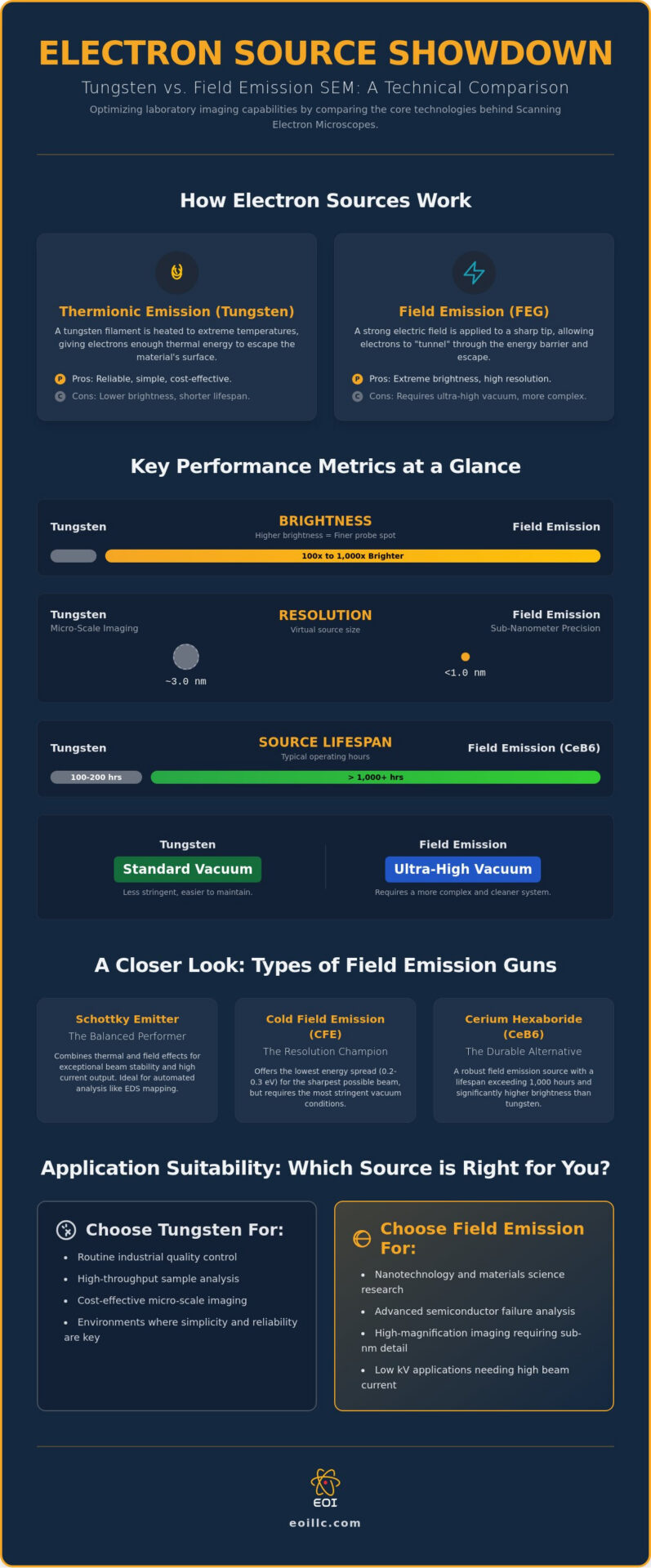
Thermionic emission involves heating a filament, typically tungsten, until the electrons gain enough thermal energy to overcome the material’s work function. In contrast, field emission sources utilize high electric fields to extract electrons via quantum tunneling from a sharp monocrystalline tip. This technical divergence results in field emission sources being 100 to 1,000 times brighter than their tungsten counterparts. It also significantly reduces the energy spread of the beam, which is vital for achieving sub-nanometer resolution in advanced hardware systems. The smaller virtual source size of a field emission gun allows for a much finer probe at the sample surface, which is the primary driver behind the superior imaging capabilities of high-end units.
The Tungsten Filament: Reliability and Simplicity
The traditional V-shaped tungsten wire remains the industry workhorse for routine industrial inspections. Its design is characterized by a high degree of reliability and a straightforward replacement process. Standard tungsten filaments operate at extreme temperatures to generate a sufficient electron flux. This creates a trade-off where higher brightness levels inevitably lead to a shorter filament life, typically ranging between 100 and 200 hours. For many quality control laboratories, the simplicity of a tungsten-based system like the Cube II Benchtop SEM or Genesis Tabletop SEM provides the necessary throughput without the complexities of ultra-high vacuum requirements. It’s a pragmatic choice for micro-scale imaging where extreme magnification isn’t the primary objective.
Field Emission Guns (FEG): The Schottky Emitter Advantage
Field emission guns represent the pinnacle of modern electron optics. Schottky emitters are particularly favored for their exceptional beam stability and high current output. They use a zirconia coating to lower the work function of the tungsten tip, combining thermal and field effects for optimized performance. When comparing the long-term utility of tungsten vs field emission sem configurations, the Schottky emitter’s ability to maintain high beam currents over extended periods makes it the preferred choice for automated EDS mapping. While Cold Field Emission (CFE) sources offer the lowest energy spread (0.2 to 0.3 eV), they require a more stringent vacuum environment. Schottky sources, found in high-performance systems like the Veritas FE SEM, offer a more balanced approach with superior long-term stability. Beyond this, Cerium Hexaboride (CeB6) sources have emerged as a robust field emission alternative, offering over 1,000 hours of lifespan and significantly higher brightness than standard tungsten filaments.
Resolution, Brightness, and Beam Stability: The Technical Divergence
The primary technical differentiator between tungsten vs field emission sem systems lies in the inherent brightness of the electron source. Field emission sources are approximately 100 to 1,000 times brighter than traditional thermionic tungsten filaments. This increased brightness is not merely a matter of intensity; it allows the electron optics to maintain a high beam current even when the probe is focused into an exceptionally small spot. When high-end systems utilize these sources, they achieve a current density that enables rapid imaging without sacrificing the signal-to-noise ratio. This is a fundamental requirement for modern laboratories where throughput and precision must coexist.
Energy spread plays a critical role in determining the final image clarity by influencing chromatic aberration. While tungsten sources typically exhibit an energy spread of 2 to 3 eV, field emission sources reduce this value significantly, with Schottky emitters operating around 0.6 to 1.1 eV and Cold Field Emission (CFE) sources reaching as low as 0.2 eV. High energy spread causes electrons to focus at different planes, which blurs the image at high magnifications. Understanding How Electron Microscopes Work reveals that minimizing this spread is the only way to maintain sharp edges and fine surface details. For researchers working with delicate or non-conductive materials, the ability of a field emission SEM to perform at low accelerating voltages, often below 5kV, is indispensable. It prevents sample charging and beam damage while providing surface-sensitive information that tungsten systems simply cannot resolve.
Beam stability is another area where the technical divergence becomes apparent during long-term analytical sessions. Tungsten filaments are subject to gradual evaporation and thermal fluctuations, leading to minor beam drift and current instability over several hours. In contrast, Schottky field emission sources are engineered for extreme stability, making them the preferred choice for automated overnight imaging or complex analytical tasks. If your facility requires this level of uncompromising stability and resolution, evaluating the Veritas FE SEM can provide a clear path toward upgrading your diagnostic capabilities.
Spatial Resolution at the Nanoscale
The ultimate spatial resolution of an SEM is dictated by the virtual source size of the electron gun. Tungsten filaments have a relatively large source size, which limits the minimum probe diameter on the sample surface and effectively caps useful magnification. Visualizing nanostructures requires the sub-nanometer probe sizes that only field emission technology can provide. High energy spread at low accelerating voltages significantly increases chromatic aberration, which inherently limits the attainable resolution of tungsten sources when imaging delicate surface features.
Performance with Energy Dispersive Spectroscopy (EDS)
Elemental mapping requires a consistent and high beam current to generate sufficient X-ray counts for accurate data. Field emission sources improve the spatial resolution of eds analysis by allowing for a smaller interaction volume within the sample. This is particularly vital when analyzing complex matrices or thin films where overlapping signals can obscure critical data. The superior stability of the FE source ensures that elemental maps remain sharp and quantitatively accurate even during extended acquisition periods.
Operational Reality: Vacuum Requirements and Filament Longevity
The operational efficiency of a laboratory is inextricably linked to the vacuum integrity required by the chosen electron source. When analyzing tungsten vs field emission sem systems, the most immediate logistical divergence is the required pressure level. Tungsten filaments operate reliably at high vacuum levels of approximately 10^-5 Torr. In contrast, field emission sources demand ultra-high vacuum (UHV) environments, often reaching 10^-9 Torr, to prevent tip contamination and ensure stable emission. This four-order-of-magnitude difference necessitates a significantly more complex and robust vacuum architecture that influences both the initial system design and long-term maintenance protocols.
Beyond vacuum levels, filament longevity represents a primary driver of total cost of ownership. A standard tungsten filament typically offers a lifespan of 100 to 200 hours before thermal evaporation leads to failure. While the individual filaments are inexpensive, the cumulative downtime required for replacement and vacuum recovery can be substantial in high-throughput industrial settings. Schottky field emission emitters provide a stark contrast, often exceeding 3,000 hours of continuous operation. This extended lifespan mitigates the need for frequent manual intervention, allowing for long-term project stability that thermionic sources simply can’t match. It’s a fundamental shift from a reactive maintenance model to one focused on sustained analytical uptime.
Vacuum System Architecture and Maintenance
Maintaining the integrity of a field emission system requires specialized hardware, most notably Ion Getter Pumps (IGP). These pumps are essential for reaching the UHV levels necessary to keep the sharp emitter tip free from residual gas molecules that would otherwise cause emission instability or tip damage. Any breach in vacuum integrity is the primary concern for FE-SEM owners, as it can lead to immediate source degradation. Comprehensive sem maintenance protocols are therefore essential to monitor pump performance and seal integrity, preventing costly unscheduled downtime and ensuring the longevity of the sophisticated electron optics.
Downtime and Service Considerations
The “real” cost of utilizing tungsten isn’t just the price of the wire; it’s the labor and lost productivity associated with vacuum recovery times. Every filament change requires venting the chamber, replacing the source, and waiting for the system to reach operational vacuum levels again. For field emission systems, while the source lasts much longer, preventative maintenance is non-negotiable to protect the specialized optics and UHV pumps. Utilizing professional SEM repair services ensures that these complex systems are calibrated to peak performance, balancing the higher initial investment with the grounded, practical realities of long-term reliability and data accuracy.
Application Suitability: When to Invest in FE-SEM vs. Tungsten
Selecting between tungsten vs field emission sem configurations requires a methodical assessment of your laboratory’s primary analytical objectives. While the pursuit of higher resolution is a common driver in equipment procurement, it is not always the most pragmatically efficient path for routine industrial environments. The decision must align with the specific material properties of your samples and the required magnification thresholds for your data to remain valid. For many organizations, the choice represents a balance between the immediate needs of production-line quality control and the long-term requirements of advanced research and development.
Industrial sectors often prioritize throughput and ease of use over the extreme resolution capabilities of field emission systems. In these scenarios, a thermionic source provides sufficient clarity for micro-scale features while maintaining a lower barrier to entry for operators. Conversely, the necessity of field emission becomes apparent when analyzing nanomaterials or complex semiconductor architectures where sub-10nm features are the primary focus. The higher brightness and lower energy spread of an FE source allow for stable imaging at low accelerating voltages, which is essential for protecting beam-sensitive biological samples or non-conductive polymers from thermal damage and charging effects.
The Case for Tungsten: Cost-Effective Reliability
Tungsten-based systems remain the definitive standard for applications such as metallurgy, basic particle sizing, and educational instruction. These environments benefit from the robust nature of the thermionic filament, which can withstand less-than-ideal sample conditions without the risk of contaminating a sensitive field emission tip. The Genesis Tabletop SEM serves as a primary example of this technology, acting as a reliable workhorse for industrial quality control. By maximizing ROI in high-volume, low-magnification environments, these systems allow laboratories to process hundreds of samples per week with minimal maintenance intervention. It’s a strategic choice for facilities where the micro-scale data is the priority and the extreme costs of ultra-high vacuum infrastructure are not technically justified.
The Case for Field Emission: Pushing the Boundaries
When “good enough” resolution fails to meet the stringent demands of modern nanotechnology, field emission is the only viable solution. Advanced failure analysis and thin-film characterization require the sub-nanometer probe sizes that only an FE source can generate. Furthermore, research grants and international publication standards increasingly favor laboratories equipped with FE-SEM capabilities, as they represent the current pinnacle of diagnostic precision. Future-proofing a facility involves recognizing that as materials science progresses toward smaller scales, the demand for low-kV performance and high-resolution mapping will only intensify. If your work demands this level of uncompromising detail, you can explore our Veritas FE SEM solutions to find the ideal match for your high-resolution imaging requirements.
Optimizing Your Laboratory with Benchtop and High-Resolution SEM Solutions
The evolution of electron microscopy in 2026 has fundamentally altered the decision matrix for laboratory procurement. While the historical debate regarding tungsten vs field emission sem often focused on a binary choice between cost and resolution, modern hardware advancements have introduced a more nuanced spectrum of capabilities. Manufacturers are now engineering systems that bridge the performance gap, integrating sophisticated automation and optimized column designs into compact footprints. This shift allows organizations to deploy high-precision imaging tools directly into production environments, ensuring that technical integration and operational excellence are achieved simultaneously.
The Cube II Benchtop SEM exemplifies this technological convergence by delivering high-performance tungsten imaging within a streamlined frame. It provides a strategic solution for facilities that require the reliability of a thermionic source without the spatial or financial demands of a traditional floor model. For laboratories seeking to push the boundaries of nanoscale characterization, the Veritas Series offers a scalable pathway. From the Veritas Pro to the specialized Veritas FE SEM, these systems provide the visionary performance required to meet the escalating standards of international research and industrial development.
Benchtop vs. Floor Model: A New Paradigm
Modern benchtop systems like the Cube II are redefining laboratory architecture by providing features once exclusive to large-scale floor models. This includes advanced vacuum management and high-sensitivity detectors that facilitate rapid sample turnaround. The trend toward decentralized microscopy allows large industrial facilities to place analytical power at the point of manufacture, reducing logistical delays. Modern, automated interfaces have also streamlined the training requirements for operators, ensuring that sophisticated imaging is accessible to a broader range of technical staff without compromising data integrity. This democratization of high-end hardware ensures that meticulousness is maintained across all levels of production.
The Veritas FE: High-Resolution Excellence
The Veritas FE SEM represents the pinnacle of the Veritas Series, featuring a column design optimized for the extreme brightness and stability of a field emission source. This hardware excels when integrated with advanced EDS systems and multi-segment detectors, providing a comprehensive platform for elemental and structural characterization. Selecting the correct configuration requires a methodical approach that considers both current imaging needs and future growth. Partnering with Electron Optics Instruments provides access to thirty years of expertise, ensuring that your procurement strategy results in a system that is perfectly aligned with your 2026 research goals and the grounded, practical realities of your facility’s operational requirements.
Advancing Laboratory Precision with Strategic Source Selection
Selecting the optimal electron source is a foundational decision that dictates the analytical trajectory of your facility. It’s a choice that impacts everything from daily throughput to the ultimate resolution of your data. While thermionic tungsten sources offer a robust and cost-effective solution for micro-scale industrial inspection, field emission technology remains the non-negotiable standard for sub-nanometer characterization. Balancing these technical requirements with the practicalities of vacuum maintenance ensures your laboratory achieves the highest standards of operational uptime. Navigating the complexities of tungsten vs field emission sem systems requires a partner with deep technical insight and a commitment to long-term reliability.
As the sole US distributor for EmCraft Scanning Electron Microscopes, we leverage over 30 years of electron optics expertise to provide comprehensive training and service for all major SEM brands. This meticulous approach ensures your technical infrastructure remains as rigorous as your research objectives. Explore our range of Benchtop and High-Resolution SEMs to identify the configuration that best aligns with your 2026 research milestones. We’re ready to help you push the boundaries of modern microscopy.
Frequently Asked Questions
What is the main difference between a tungsten and field emission SEM?
The fundamental distinction between tungsten vs field emission sem systems lies in the physical mechanism used to liberate electrons. Tungsten sources rely on thermionic emission, where a filament is heated to extreme temperatures to overcome the material’s work function. Field emission guns utilize a high electric field to extract electrons via quantum tunneling from a sharp monocrystalline tip, resulting in a source that is significantly brighter and possesses a much smaller virtual source size for superior resolution.
How much more expensive is a field emission SEM compared to a tungsten model?
Field emission models represent a higher capital investment compared to tungsten units because of the sophisticated ultra-high vacuum infrastructure and advanced electron optics they demand. While a tungsten-based system like the Cube II is highly cost-effective for routine industrial quality control, the Veritas FE SEM requires a larger initial expenditure. This investment reflects the superior resolution and long-term analytical stability provided by field emission technology in high-end research and nanotechnology environments.
How long does a tungsten filament typically last in an SEM?
A standard tungsten filament typically operates for 100 to 200 hours before thermal evaporation leads to physical breakage. This lifespan depends heavily on the operating temperature and the vacuum quality maintained within the gun chamber. In high-throughput laboratories, this necessitates frequent downtime for filament replacement and subsequent vacuum recovery, which can impact overall laboratory efficiency if not managed through a structured maintenance schedule and a consistent supply of consumables.
Can I upgrade a tungsten SEM to a field emission source later?
It’s generally not possible to upgrade a tungsten SEM to a field emission source due to the fundamental differences in vacuum requirements and column architecture. Field emission sources require ultra-high vacuum levels, often reaching 10^-9 Torr, which standard tungsten chassis aren’t engineered to maintain. The entire electronic control system and lens configuration are also specifically tuned to the source’s unique brightness and energy spread, making a retrofit technically and financially impractical for most facilities.
Why is vacuum quality more critical for FE-SEM than for tungsten?
Vacuum quality is critical for FE-SEM because the sharp emitter tip is extremely sensitive to contamination and ion bombardment. Residual gas molecules in a lower-quality vacuum can be ionized by the electron beam and accelerated back toward the tip, causing physical damage or emission instability. Maintaining an ultra-high vacuum environment using ion getter pumps is the only way to preserve the tip’s sharpness and ensure the long-term stability required for nanoscale imaging.
Which SEM source is better for Energy Dispersive Spectroscopy (EDS)?
Schottky field emission sources are superior for Energy Dispersive Spectroscopy (EDS) due to their high beam current and exceptional stability over long acquisition periods. While tungsten can provide sufficient current for basic analysis, the larger spot size limits the spatial resolution of the resulting elemental maps. An FE-SEM allows for high-count rates with a much smaller interaction volume, which is vital for identifying elemental distributions in complex or nanoscale matrices.
Is an FE-SEM necessary for imaging biological samples?
An FE-SEM is highly advantageous for biological samples because of its superior performance at low accelerating voltages. Biological tissues are often beam-sensitive and non-conductive, leading to charging and thermal damage under standard tungsten beams. The high brightness of a field emission source allows for clear, high-resolution imaging at 1kV to 5kV, which preserves delicate surface structures and significantly reduces the need for heavy conductive coatings that might obscure fine details.
What are the maintenance requirements for a Schottky field emission gun?
Maintenance for a Schottky field emission gun focuses primarily on preserving vacuum integrity and monitoring high-voltage stability within the column. Unlike tungsten filaments that require frequent replacement, a Schottky tip can last over 3,000 hours with proper care and consistent vacuum levels. This involves regular preventative maintenance visits to inspect ion getter pumps and ensuring the system isn’t vented unnecessarily, as any exposure to atmosphere can compromise the specialized zirconia-coated emitter.