
What if the high-resolution data you expect from your electron microscope is being systematically masked by the very preparation steps you rely on? The true microstructure of an advanced material is frequently compromised by traditional preparation techniques, leading to significant surface deformation that obscures critical analytical data. You’ve likely encountered promising specimens ruined by surface smearing, a common barrier that prevents your equipment from reaching its full potential. Mastering ion milling for sem samples is no longer a luxury for specialized research; it is the essential bridge between sophisticated hardware and actionable microstructural insights.
This guide delivers the technical expertise required to eliminate these subsurface distortions and maximize the performance of high-end systems such as the Veritas HR SEM. You’ll gain a comprehensive understanding of the strategic nuances between Broad Ion Beam (BIB) and Focused Ion Beam (FIB) technologies while examining the specific parameters necessary to streamline your prep-to-imaging workflow. By the end of this analysis, you’ll possess the methodological framework to achieve pristine, artifact-free surfaces that meet the rigorous standards of 2026 microscopy.
Key Takeaways
- Identify the critical limitations of traditional mechanical polishing, such as surface smearing and grain plucking, that obscure the true microstructural characteristics of advanced materials.
- Understand the atomic-level mechanics of argon ion sputtering to achieve precise, non-contact material removal while maintaining the structural integrity of delicate specimens.
- Evaluate the strategic ROI of implementing ion milling for sem samples to unlock the full analytical potential of high-performance systems like the Veritas series.
- Master the geometric nuances of glancing versus steep incidence angles to optimize the preparation of heterogeneous materials and multi-layer thin films.
- Streamline laboratory workflows by integrating standardized milling protocols that ensure consistent, artifact-free surfaces for high-resolution EBSD mapping and failure analysis.
The Evolution of Sample Preparation: Why Standard Methods Fall Short in 2026
The strategic implementation of ion milling for sem samples facilitates a transition from macro-scale abrasive techniques to atomic-level refinement. This methodology employs a kinetic sputtering process where accelerated argon ions strike the specimen surface, ejecting atoms through precise momentum transfer. It’s a non-contact, dry etching technique that eliminates the contamination risks inherent in fluid-based slurries. By targeting surface atoms with meticulous precision, researchers achieve a level of cleanliness that mechanical methods cannot approximate. In the rigorous landscape of 2026 microscopy, this precision is the standard for reliable data.
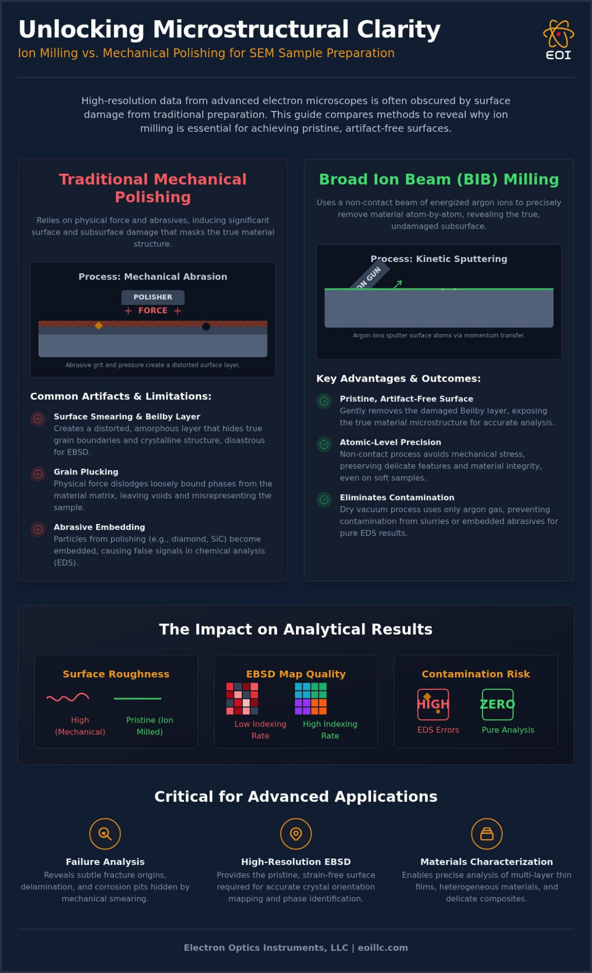
Traditional mechanical grinding relies on physical grit and compressive force. This approach frequently results in grain plucking, where loosely bound phases are dislodged from the matrix, or the embedding of abrasive particles like diamond or silicon carbide. Such artifacts don’t just compromise aesthetics; they introduce false signals that complicate Energy Dispersive Spectroscopy (EDS) and obscure the true stoichiometry of sensitive materials.
The Problem of Mechanical Deformation
Mechanical stress alters the underlying crystalline lattice, creating a highly distorted surface layer known as the Beilby layer. This amorphous zone masks true grain orientations, which is particularly detrimental to Electron Backscatter Diffraction (EBSD). When surface smearing occurs, indexing rates plummet, making it impossible to map crystal orientation with accuracy. Soft materials, including lead, gold, and various polymers, are exceptionally vulnerable to these preparation-induced artifacts. Their low yield strength allows for significant plastic deformation, which effectively hides the true microstructure under a layer of displaced material.
Transitioning from Macro to Nano-Scale Preparation
As modern SEM resolution reaches the sub-nanometer range, the requirements for surface roughness have become significantly more stringent. Achieving the full analytical potential of the Veritas Series SEM demands a surface that is pristine at the molecular level. Poor preparation leads to misinterpreted data and costly errors in failure analysis. If the specimen surface fails to represent the bulk material, the integrity of the entire technical investigation is compromised. Ion milling provides the necessary bridge to ensure that your imaging reflects the actual material state, reinforcing the synergy between advanced hardware and logistical excellence.
Fundamental Mechanics: The Science of Broad Ion Beam (BIB) Milling
The fundamental efficacy of ion milling for sem samples resides in the controlled kinetic interaction between accelerated noble gas ions and the target material lattice. Unlike chemical etching, Broad Ion Beam (BIB) milling utilizes argon ions to physically displace surface atoms through a mechanism known as momentum transfer. This process is orchestrated within a vacuum chamber where an ion source generates a collimated beam directed at the specimen. The resulting impact initiates a collision cascade, ejecting material at the atomic level to reveal the pristine subsurface structures required for advanced analytical characterization.
The Sputtering Process and Ion Optics
The precision of the sputtering process is governed by the modulation of beam energy, typically ranging from 0.1 keV to 8 keV. Higher energy levels facilitate rapid material removal but increase the risk of amorphization, a state where the crystalline surface becomes disordered. Expert operators must balance throughput with structural integrity by gradually reducing voltage during the final stages of preparation. Maintaining beam uniformity across the entire milling area is essential for large-scale applications. It prevents localized over-etching and ensures that the data collected from the center of the sample is consistent with the periphery. If you’re looking to upgrade your laboratory’s capabilities, exploring expertly maintained SEM systems can provide the necessary stability for these sensitive operations.
Geometry plays a decisive role in determining the final surface topography. Glancing angles, often between 1 and 6 degrees, are utilized for flat milling to achieve sub-nanometer roughness. Conversely, steep incidence angles are employed for cross-sectional milling, where a shielding mask is often used to create a clean, vertical cut through heterogeneous layers. For heat-sensitive materials, such as polymers or low-melting-point alloys, managing the thermal energy generated by ion impact is vital. Cryogenic cooling stages utilize liquid nitrogen to maintain sample stability, preventing phase transformations that would otherwise invalidate the microstructural analysis.
Minimizing Ion-Induced Artifacts
Even with advanced optics, ion-induced artifacts like curtaining can manifest during cross-sectioning. This phenomenon occurs when variations in sputtering rates across different phases create vertical striations. To mitigate this, modern systems employ sample rotation or high-frequency oscillation, which varies the ion incidence direction and averages out the sputtering effects. A low-energy final polish, often performed at less than 500 eV, is the definitive step in removing any residual damaged layers. This meticulous approach ensures that the resulting surface is a true representation of the bulk material, ready for high-resolution imaging.
Strategic Comparison: Ion Milling vs. Mechanical Polishing Frameworks
Mechanical polishing provides a robust solution for bulk material removal, yet its inherent limitations in precision necessitate a strategic shift toward ion milling for sem samples when high-resolution data is the primary objective. Evaluating the Total Cost of Ownership (TCO) for preparation equipment involves analyzing not just the initial capital expenditure, but the long-term operational efficiency gained through reduced sample rejection rates. While mechanical methods are often perceived as faster, the hidden costs of misinterpreted data and repeated imaging sessions can quickly erode those perceived gains. A visionary laboratory prioritizes preparation techniques that guarantee the integrity of the results from the first scan.
Throughput and Precision Trade-offs
The ROI of ion milling is realized through the elimination of preparation-induced artifacts, which significantly reduces re-scan rates in high-demand environments. While mechanical polishing sequences offer high throughput for routine metallurgical inspections, they often fail to meet the sub-nanometer requirements of 2026 failure analysis. When factoring in the overall electron microscope cost and laboratory overhead, the hours spent in an automated ion miller are often more economical than the manual labor required for iterative mechanical polishing that may still result in a sub-optimal surface. Precision preparation ensures that the performance of high-end hardware is never throttled by poor sample quality.
The Decision Matrix for Advanced Materials
Choosing the appropriate preparation method depends heavily on the material’s mechanical properties and the desired analytical outcome. In semiconductor failure analysis, the necessity to visualize multi-layer thin films without interfacial smearing makes ion milling the only viable option. Similarly, battery research involving lithium-ion components requires cross-sectional milling to preserve the delicate interface between the electrode and current collector. For composite materials with varying hardness levels, mechanical polishing often creates relief effects where softer phases are eroded faster than harder inclusions. Ion milling bypasses this issue by utilizing atomic sputtering that is less sensitive to differential hardness, ensuring a perfectly planar surface across heterogeneous boundaries.
Hybrid workflows represent the pinnacle of logistical excellence in modern microscopy. By utilizing mechanical grinding for rapid bulk removal and finishing with a low-energy ion polish, labs maximize throughput while maintaining the artifact-free surfaces necessary for EBSD and high-resolution imaging. This methodology balances the grounded realities of production speed with the uncompromising standards of international research capability.
Critical Applications in Failure Analysis and Material Characterization
The deployment of ion milling for sem samples is a prerequisite for any laboratory focused on the microstructural authenticity of complex material systems. In the context of 2026 industrial standards, the ability to resolve multi-layer thin films and coatings without interfacial smearing is a baseline requirement for quality assurance. Beyond mere imaging, ion milling serves as the definitive preparation method for Electron Backscatter Diffraction (EBSD). By removing the amorphous layer generated during mechanical grinding, this process enables the acquisition of high-fidelity crystal orientation data. This is essential for analyzing grain boundaries and phase distributions in advanced metallurgy where precision is paramount.
Semiconductor and Microelectronics Analysis
Identifying failures in integrated circuits requires a preparation method that preserves the delicate geometry of gate structures and interconnects. Traditional mechanical polishing often causes “dragging” of ductile metals across insulating layers, leading to false positives in failure investigations. Ion milling eliminates this risk, facilitating the precise exposure of internal voids or subsurface contamination. This level of surface cleanliness is particularly beneficial when paired with EDS (Energy Dispersive Spectroscopy). It ensures that the detected X-ray signals originate from the true material composition rather than embedded abrasives or smeared surface layers. For organizations seeking to optimize their failure analysis protocols, you can browse our full catalog of high-performance SEM systems designed for advanced characterization.
Energy Storage and Battery Research
The rapid evolution of battery technology demands specialized preparation techniques to visualize the solid electrolyte interphase (SEI) and delicate electrode boundaries. Battery components are notoriously sensitive to mechanical stress and atmospheric exposure. Cross-sectional ion milling provides the necessary precision to reveal delamination or crack propagation within the cathode/anode layers without introducing preparation-induced damage. For air-sensitive materials, integrating an inert gas transfer system ensures that the milled surface remains pristine from the preparation chamber to the SEM vacuum. This meticulous approach is vital for characterizing the structural degradation of Li-ion cells over extended cycling.
Geological and ceramic studies also benefit significantly from this non-contact approach. Brittle structures, which would typically shatter or pluck under mechanical pressure, are preserved in their native state. This allows for accurate porosity analysis and mineralogical mapping in samples that would otherwise be impossible to prepare. By maintaining the structural integrity of these fragile materials, researchers can gain insights into pore connectivity and mineral distribution that are critical for both energy extraction and advanced ceramic engineering.
Optimizing Workflows with Advanced SEM Instrumentation
The strategic deployment of ion milling for sem samples is only as effective as the hardware utilized for the final analysis. In a modern laboratory, the synergy between preparation and imaging defines the upper limit of microstructural characterization. When utilizing a high-performance system like the Cube II Benchtop SEM, the quality of surface preparation becomes the primary determinant of analytical success. Integrating these prep steps into a standardized SEM operation protocol ensures that the data remains reproducible across different shifts and operators.
Maximizing Benchtop SEM Performance
A common misconception in the industry is that benchtop microscopes don’t require high-end sample preparation. In reality, the opposite is true. Because these units are designed for rapid throughput, a pristine milled surface allows the electron optics to operate at peak efficiency without the interference of surface artifacts. Electron Optics Instruments, LLC addresses this need through comprehensive on-site technical training, ensuring that your team masters the delicate balance of beam energy and milling time to achieve repeatable results. This expertise reduces the failure rates associated with manual polishing and accelerates the transition from sample receipt to final report.
Selecting the appropriate SEM model is a critical strategic decision for any facility. While the Genesis series offers exceptional versatility for general material characterization, the Veritas series is engineered for the extreme resolution requirements that follow meticulous ion milling for sem samples. The Veritas HR and FE models provide the stability and signal-to-noise ratios necessary to resolve the sub-nanometer features exposed by atomic sputtering. Matching your prep capabilities with the correct imaging platform builds a microscopy ecosystem that’s both resilient and visionary, ensuring your hardware is never the bottleneck for your analytical goals.
Ensuring Long-Term Precision
Maintaining the resolution gained through advanced preparation requires a commitment to rigorous SEM maintenance. Even the most perfectly milled sample will yield poor data if the electron column is misaligned or the filaments are degraded. Preventative service contracts acts as a safeguard for your technical investment, ensuring that both your preparation equipment and your imaging hardware operate in perfect synchronization. Partnering with Electron Optics Instruments, LLC provides access to over 30 years of industry expertise, offering a holistic approach to microscopy that balances industrial performance with logistical excellence.
Advancing Microstructural Accuracy Through Atomic Precision
Achieving the sub-nanometer resolution required by modern industrial standards necessitates a departure from traditional mechanical constraints. As we’ve explored, the implementation of ion milling for sem samples is the definitive methodology for exposing the true stoichiometry of advanced materials without the interference of preparation-induced artifacts. By transitioning to atomic-level sputtering, your laboratory ensures that every scan reflects the authentic state of the specimen, whether you’re characterizing complex battery interfaces or semiconductor gate structures.
Success in this technical landscape depends on the synergy between expert preparation and high-performance hardware. Electron Optics Instruments provides the foundational support necessary to master these workflows. With over 30 years of industry experience and our status as the sole US distributor for EmCraft, we offer the technical training and national service support required to maintain your competitive edge. Consult with our SEM experts to optimize your sample preparation workflow and unlock the full potential of your analytical systems. Your journey toward pristine, high-resolution imaging begins with meticulous preparation.
Frequently Asked Questions
What is the primary difference between Broad Ion Beam (BIB) and Focused Ion Beam (FIB)?
The primary distinction lies in the scale and precision of the material removal area. Broad Ion Beam (BIB) systems utilize a millimetre-scale beam to polish large surface areas or create extensive cross-sections. In contrast, Focused Ion Beam (FIB) technology employs a high-precision, nanometre-scale beam for site-specific micro-machining and TEM lamella preparation. While FIB offers surgical accuracy for localized defects, BIB provides the throughput necessary for comprehensive microstructural characterization across heterogeneous bulk specimens.
Can ion milling damage my SEM samples?
While ion milling for sem samples is designed to minimize prep-induced artifacts, improper parameter selection can lead to surface damage. Excessive beam energy often results in amorphization, where the crystalline structure of the top atomic layers is disordered. Additionally, high-current milling can generate localized heat, potentially causing phase transformations in polymers or low-melting-point alloys. Utilizing cryogenic cooling and low-voltage final polishing steps effectively mitigates these risks, ensuring the structural integrity of the specimen.
How long does a typical ion milling process take for a metal sample?
Processing times vary significantly based on material hardness, beam current, and the required depth of removal. A typical argon ion milling sequence for a metallurgical specimen ranges from 30 minutes to 4 hours. Soft metals like gold or lead require less time, while refractory metals such as tungsten or hardened steel necessitate longer durations to achieve a planar finish. Automated systems allow for unattended operation, which helps maintain laboratory throughput despite these extended preparation cycles.
Is ion milling necessary for all types of SEM imaging?
Ion milling isn’t a universal requirement for every SEM application, but it’s vital for high-resolution analytical microscopy. Robust materials with coarse features might only require traditional mechanical polishing. However, advanced techniques such as EBSD, multi-layer coating analysis, and the characterization of porous ceramics demand the atomic-level cleanliness that only ion sputtering provides. For laboratories utilizing high-performance hardware like the Veritas FE SEM, this preparation step is essential to justify the equipment investment.
What are the most common artifacts produced by ion milling and how can I avoid them?
The most frequent artifacts include “curtaining” and surface amorphization. Curtaining appears as vertical striations during cross-sectioning and is typically avoided by employing sample rotation or high-frequency oscillation during the milling process. Surface amorphization, caused by high-energy ion impact, is corrected by a low-energy final polish, often below 500 eV. Managing thermal artifacts is also critical, particularly for heat-sensitive samples, where integrated liquid nitrogen cooling systems prevent melting or structural degradation during the process.
Do I need special training to operate an ion milling system?
Professional operation of an ion milling system requires specialized knowledge of vacuum physics, ion optics, and material science. Understanding how to modulate voltage and incidence angles is critical for achieving repeatable results. Electron Optics Instruments provides comprehensive on-site technical training as part of our commitment to laboratory excellence. This education ensures that staff can effectively integrate ion milling for sem samples into their standard operating procedures, reducing sample failure rates and optimizing imaging outcomes.
How does ion milling improve EBSD results?
Ion milling is considered the gold standard for EBSD because it removes the mechanically deformed surface layer that inhibits electron diffraction. Mechanical polishing often leaves a thin amorphous zone, known as the Beilby layer, which prevents the formation of clear Kikuchi patterns. By utilizing argon ion sputtering to reveal the pristine crystalline lattice, researchers significantly increase indexing rates and spatial resolution. This results in more accurate grain orientation maps and superior phase identification data.
What is the cost-to-benefit ratio of ion milling for a small research lab?
For a small research facility, the ROI is realized through the elimination of misinterpreted data and the reduction of costly re-imaging sessions. High-quality preparation ensures that even benchtop systems like the Cube II can deliver results comparable to floor-standing units. While the initial capital expenditure is a factor, the long-term benefit of providing actionable, artifact-free data to industrial partners often outweighs the cost. It’s a strategic investment in technical authority and long-term analytical reliability.