

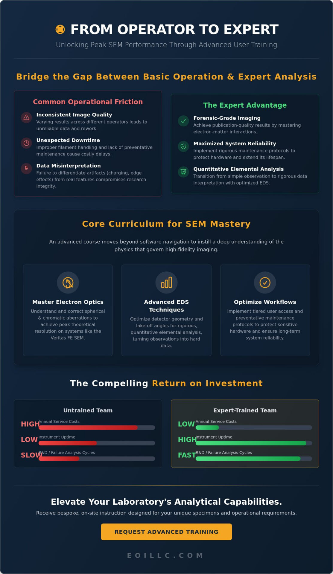
True mastery of scanning electron microscopy transcends the simple navigation of a software interface; it requires a profound understanding of electron-matter interactions to convert raw data into definitive industrial intelligence. You’ve likely experienced the operational friction caused by inconsistent image quality across different operators or the unexpected downtime resulting from improper filament handling. These technical bottlenecks often prevent laboratories from achieving the forensic-grade imaging necessary for high-stakes failure analysis. Within this context, an advanced sem user training course provides the necessary framework to elevate your laboratory’s analytical capabilities and ensure that sophisticated hardware, such as the Veritas Ultra SEM, operates at its peak theoretical resolution.
This article examines the strategic methodologies for refining instrument optimization, mastering complex EDS data interpretation, and implementing rigorous maintenance habits to secure long-term system reliability. We’ll explore how shifting from basic operation to expert-level characterization reduces long-term costs while fostering a culture of technical meticulousness. In a global nanotechnology market now exceeding 125 billion dollars, achieving publication-quality results is not a matter of chance; it is the result of disciplined training and a deep synergy between the operator and the hardware.
Key Takeaways
- Master the physics of electron optics, including spherical and chromatic aberration correction, to achieve the highest possible resolution on high-end hardware like the Veritas FE SEM.
- Transition from qualitative observations to rigorous quantitative elemental analysis by optimizing Energy Dispersive Spectroscopy (EDS) geometry and detector take-off angles.
- Protect sensitive hardware configurations and minimize unplanned downtime through the implementation of tiered user access systems and rigorous preventative maintenance protocols.
- Utilize an advanced sem user training course to receive bespoke, on-site instruction specifically designed for your laboratory’s unique specimen types and operational requirements.
- Enhance organizational throughput by transforming complex electron-matter interactions into the forensic-grade data required for sophisticated industrial failure analysis.
The Strategic Value of Advanced Scanning Electron Microscopy Training
The evolution of a laboratory’s analytical capacity depends heavily on the professional development of its technical staff. Moving beyond basic instrument operation requires a fundamental shift in perspective. An operator manages the interface, but a microscopist masters the Scanning Electron Microscope as a precision instrument for comprehensive material characterization. This transition is essential in high-tech sectors where even minor data inaccuracies lead to systemic failures in production or research. Investing in an advanced sem user training course catalyzes this transformation, providing the theoretical depth required to optimize instrument performance under non-standard conditions.
While basic manufacturer orientations provide a necessary introduction to safety and basic navigation, they rarely address the nuanced challenges of complex specimen interaction or the physics of signal generation. Participation in an advanced sem user training course equips a team with the technical authority to interpret data with forensic precision. This meticulousness ensures that results aren’t just visually impressive but scientifically valid. Such expertise is indispensable for maintaining ISO compliance and adhering to rigorous industry-specific standards that govern international production quality and logistical excellence.
Bridging the Gap Between Basic Operation and Expert Analysis
Relying on ‘auto-mode’ functions often obscures critical topographic or compositional details in high-resolution environments. Automation is designed for broad consistency; it isn’t optimized for the unique challenges of non-conductive samples or beam-sensitive materials. By mastering advanced sem techniques, users gain a competitive advantage through the ability to manipulate beam parameters to suit specific analytical objectives. Expert-level training provides the diagnostic skills needed to differentiate between genuine morphological features and imaging artifacts like charging, edge effects, or carbon contamination. These phenomena frequently lead to misinterpretation in less experienced hands, potentially compromising the integrity of a research project.
Economic Benefits of a Highly Skilled Microscopy Team
The financial narrative for specialized training is as compelling as the technical one. A team that possesses deep instrument knowledge significantly reduces annual service costs. These users implement superior preventative maintenance habits, such as meticulous filament alignment and aperture management, which directly extend the lifespan of expensive consumables. Additionally, the ability to perform in-house forensic-level failure analysis accelerates R&D cycles. Instead of outsourcing critical characterization to third-party labs, organizations achieve a steady flow of actionable intelligence. This synergy between technical proficiency and operational efficiency ensures that high-end systems, such as the Veritas Pro SEM, deliver a superior return on investment through maximized uptime and precision.
Core Curriculum: Mastering Electron Optics and Vacuum Dynamics
Achieving high-fidelity results requires more than a cursory knowledge of software toggles; it demands a rigorous understanding of the internal physics governing the electron column. An advanced sem user training course delves into the complex mechanics of signal generation, focusing on how electron beam interactions vary across diverse specimen types. This involves analyzing the interaction volume, where the accelerating voltage (kV) and probe current must be meticulously balanced to prevent beam damage in sensitive materials. By mastering these parameters, a microscopist can maximize the signal-to-noise ratio in both secondary and backscattered modes, ensuring that every pixel contributes to a technically accurate representation of the sample surface.
The curriculum also addresses the fundamental limitations of electromagnetic lenses, specifically focusing on spherical and chromatic aberration correction. These phenomena are the primary inhibitors of resolution at high magnifications. Understanding the underlying optics allows operators to push the limits of their hardware, such as the Veritas HR SEM, to achieve the sub-nanometer precision required for modern semiconductor or metallurgical analysis. For those seeking a foundational review of these principles, the University of Minnesota’s SEM Primer provides an excellent technical overview of the primary beam’s behavior within the column.
Advanced Beam Manipulation and Alignment
Precision imaging is impossible without perfect column alignment. At low voltages, even minor misalignments result in significant resolution loss. Training focuses on the iterative process of centering the beam and correcting astigmatism, which is vital for maintaining image clarity as magnification increases. These techniques are especially critical when mitigating sample charging in non-conductive materials. By manipulating the scan rate and beam energy, experts can stabilize the surface potential, allowing for high-resolution characterization without the need for conductive coatings that might obscure fine topographical details.
Vacuum System Management and Troubleshooting
The relationship between pressure and the mean free path of electrons is a cornerstone of microscopy that is often overlooked in basic orientations. A robust sem vacuum system is essential for preventing electron scattering and column contamination. Participants learn to identify early indicators of vacuum leaks, such as fluctuating ion pump currents or extended pump-down times, before they lead to catastrophic system shutdowns. Best practices for sample outgassing and chamber cleanliness are also emphasized, ensuring that the internal environment remains pristine for high-sensitivity detectors. If you’re looking to upgrade your laboratory’s infrastructure, exploring refurbished SEM units can provide access to high-vacuum capabilities at a strategic price point.
Advanced Analytical Techniques: Beyond Topographical Imaging
High-resolution imaging provides the morphological foundation for research, yet the true potential of modern instrumentation lies in its analytical depth. To transform a standard laboratory into a center of excellence, operators must look beyond surface topography to understand the underlying chemical and structural composition of their materials. An advanced sem user training course facilitates this transition by providing the theoretical framework necessary to master Energy Dispersive Spectroscopy (EDS) and Backscattered Electron (BSE) imaging. These techniques allow for the precise identification of phases and elemental distributions, which are essential for validating the integrity of high-performance components. Similar technical rigor is reflected in the EPFL Scanning Electron Microscopy Techniques Course, which emphasizes the synergy between imaging modes and analytical data collection.
Backscattered electron imaging serves as a critical bridge between visual inspection and chemical mapping. By leveraging Z-contrast, where higher atomic number elements appear brighter, microscopists can rapidly identify inclusions or secondary phases in complex alloys. This compositional contrast is particularly valuable when paired with optimized detector geometry. Adjusting the take-off angle and working distance ensures that X-ray collection is maximized, reducing spectral noise and improving the accuracy of quantitative results. Mastering these variables allows for the generation of forensic-grade data that can withstand the scrutiny of international production standards.
Mastering Chemical Characterization with EDS
Effective elemental analysis requires a sophisticated understanding of detector physics and signal processing. Training programs focus on managing dead time and pulse processing to ensure that high-count rates don’t lead to spectral distortion. In complex alloys, identifying spectral interference and peak overlaps is vital for accurate quantification. Users learn the nuances of standardless versus standardized analysis, ensuring that the data generated by their EDS (Energy Dispersive Spectroscopy) Systems meets the stringent requirements of industrial quality control. Mapping and line scan techniques further enable the observation of diffusion gradients and interfacial reactions, providing a dynamic view of material behavior.
Failure Analysis and Forensic Microscopy
In the B2B sector, the primary objective of advanced microscopy is often failure analysis. This requires a systematic approach to identifying the root causes of fatigue, corrosion, and manufacturing defects. By utilizing a high-resolution platform like the Veritas Ultra SEM, investigators can perform gate-level inspections in semiconductor devices or analyze micro-fractures in aerospace components. Integrating this SEM data into comprehensive forensic reports allows organizations to implement corrective actions that prevent future operational failures. This methodical characterization ensures that every analysis contributes to the long-term reliability and progress of the industrial enterprise.
Optimizing Laboratory Workflows and Instrument Longevity
Operational excellence in a high-tech facility requires more than individual expertise; it demands a structured environment where hardware and data are managed with meticulousness. An advanced sem user training course provides the strategic framework for establishing these institutional standards. By implementing a tiered user access system, laboratory managers can protect sensitive hardware configurations on advanced platforms, such as the Veritas HR SEM, ensuring that only qualified personnel manipulate critical alignment parameters. This level of control is fundamental to maintaining the long-term stability of the instrument and the integrity of the analytical output across multi-user environments.
Central to this strategy is the implementation of a rigorous sem maintenance protocol. Such a schedule minimizes unplanned downtime by identifying potential mechanical or electronic instabilities before they manifest as system failures. Standardizing imaging protocols across different shifts ensures data reproducibility, a critical requirement for long-term research projects or industrial quality control. Additionally, mastering advanced sample preparation techniques, such as ion milling or precise cross-sectioning, allows the team to present the hardware with the highest quality specimens, thereby maximizing the resolution potential of the system. Secure digital data management and metadata preservation further ensure that every session contributes to a robust audit trail for industrial compliance.
Standard Operating Procedures (SOPs) for High-Performance Labs
High-performance labs thrive on consistency. Creating custom checklists for specific material classes, whether polymers, metals, or ceramics, prevents the application of incorrect beam parameters that could lead to sample damage or data artifacts. Regular magnification calibration and system validation are not merely suggestions; they’re requirements for maintaining the audit trails necessary for international industrial compliance. Training staff on the nuances of low-vacuum operation further expands the lab’s versatility, allowing for the characterization of outgassing samples without compromising the safety of the detector systems.
Proactive Hardware Care and Consumable Optimization
Proactive hardware management is the most effective method for consumable optimization. Within an advanced sem user training course, participants learn the delicate physics of filament saturation. This knowledge directly extends the operational life of tungsten and LaB6 filaments, reducing the frequency of chamber venting and the associated risk of contamination. Regular cleaning and maintenance of apertures prevents beam drift and distortion, maintaining the precision required for sub-nanometer characterization. For organizations looking to secure their operational continuity, scheduling Preventative Maintenance Visits ensures that every component is calibrated to its peak theoretical performance.
Bespoke On-Site Training Solutions from Electron Optics Instruments, LLC
Generic educational programs often follow a rigid, manufacturer-specific syllabus that fails to account for the unique sample types and environmental variables of a working industrial laboratory. Electron Optics Instruments, LLC addresses this gap by offering a highly specialized advanced sem user training course delivered directly at your facility. This on-site methodology ensures that your team masters precision microscopy using the exact hardware and software configurations they encounter during daily operations. Whether your laboratory utilizes the compact Cube II Benchtop SEM or the ultra-high resolution Veritas FE SEM, our curriculum is tailored to the specific material classes and analytical objectives of your organization.
The primary advantage of on-site instruction is the ability to perform characterization on your own specimens. This eliminates the technical translation gap that occurs when operators move from a training center’s ideal samples to the complex, often challenging materials found in their own production lines. Our instructors provide comprehensive post-training support and advanced technical integration consulting, ensuring that your instrumentation remains a source of verifiable industrial intelligence. By training across multiple platforms, including the Genesis and Veritas series, we provide a unified standard of excellence that transcends individual machine limitations.
Why Industrial Leaders Choose EOI for Technical Education
With over 30 years of cross-manufacturer expertise in electron optics, Electron Optics Instruments, LLC bridges the divide between theoretical physics and practical logistical excellence. Our instruction covers the entire operational lifecycle, integrating foundational principles with the practicalities of sem repair services and long-term hardware preservation. This holistic approach ensures that your staff doesn’t just operate the system but understands the mechanical and electronic precursors to system instability. We offer flexible scheduling to minimize the impact on your facility’s operational output, allowing for technical advancement without compromising critical production deadlines.
Scheduling Your Advanced SEM Consultation
The process begins with a rigorous assessment of your team’s current proficiency and your laboratory’s specific characterization needs. This allows us to design an advanced sem user training course that targets existing skill gaps and maximizes the utility of your specific detectors and analytical software. Integrating this on-site education with existing annual service contracts provides maximum value, reinforcing the synergy between user proficiency and instrument longevity. By elevating your internal expertise, you reduce reliance on external service providers and secure a more resilient research and development pipeline.
Contact EOI, LLC to design your customized advanced training program and elevate your laboratory’s analytical standards for 2026.
Advancing Industrial Intelligence Through Technical Mastery
The transformation of a laboratory from a standard testing facility into a strategic asset depends upon the continuous refinement of its technical personnel. Mastering the complexities of electron-matter interactions and signal generation allows microscopists to transcend basic topographical imaging and deliver the forensic-grade data required for sophisticated industrial failure analysis. By implementing the rigorous maintenance protocols and standardized workflows discussed, your team ensures that high-performance systems maintain their peak theoretical resolution while significantly reducing long-term operational costs and unplanned downtime.
Enrolling in an advanced sem user training course facilitates this institutional growth. With over 30 years of industrial microscopy expertise and our position as the sole US distributor for EmCraft SEMs, Electron Optics Instruments, LLC provides comprehensive support for all major SEM brands. We invite you to Request a Tailored Proposal for Advanced SEM Training to begin the strategic elevation of your laboratory’s analytical standards. Achieving the next tier of precision is a methodical journey that starts with a commitment to technical excellence and professional meticulousness.
Frequently Asked Questions
What is the difference between basic and advanced SEM training?
Basic training typically focuses on instrument safety and graphical user interface navigation; whereas an advanced sem user training course explores the physics of electron-matter interactions and beam optimization. This higher-level instruction enables operators to manipulate accelerating voltage and probe current to achieve sub-nanometer resolution on complex specimens. By moving beyond automated settings, users gain the ability to troubleshoot imaging artifacts and interpret compositional data with forensic precision.
Can you provide training for SEM models not sold by EOI, such as JEOL or Hitachi?
Yes, our technical specialists provide comprehensive instruction for all major electron microscope brands, including JEOL and Hitachi platforms. Our 30 years of industrial experience allow us to apply universal principles of electron optics to any specific hardware configuration. This cross-manufacturer expertise ensures that your team maintains a high standard of analytical meticulousness regardless of the specific instrumentation currently integrated into your laboratory’s workflow.
How long does a typical advanced on-site training course last?
A typical on-site engagement for an advanced sem user training course spans two to three consecutive days of intensive instruction. This duration allows for a balanced blend of theoretical lectures and hands-on application using your facility’s specific hardware and samples. We customize the timeline based on your team’s current proficiency and the complexity of the analytical techniques, such as EDS or low-vacuum operation, that require mastery.
Is sample preparation included in the advanced user training curriculum?
Sample preparation is a fundamental component of our advanced curriculum because the quality of the specimen directly dictates the resolution of the final image. We provide instruction on advanced techniques such as cross-sectioning, ion milling, and conductive coating optimization. Mastering these preparatory steps is essential for achieving the forensic-grade data required in high-stakes industrial failure analysis and material characterization.
Do you offer certifications for users who complete the advanced SEM course?
We provide a formal certificate of completion for all participants who successfully finish the training program to document their technical proficiency. While there is no universal legal certification for SEM operation, our documentation serves as a verifiable record of professional development within your organization’s quality management system. This helps maintain compliance with internal ISO standards and demonstrates a commitment to technical excellence in specialized industrial sectors.
How many staff members can participate in a single on-site training session?
We generally recommend limiting on-site sessions to three to five participants to ensure that every staff member receives sufficient hands-on time with the instrument. This small group size facilitates a more interactive learning environment where specific technical questions can be addressed in detail. If your organization requires training for a larger department, we can arrange multiple sessions to maintain the instructional quality and technical depth required for mastery.
Can the training be focused specifically on EDS and elemental analysis?
Yes, the curriculum can be specifically tailored to focus on our EDS (Energy Dispersive Spectroscopy) Systems and advanced elemental analysis. This includes in-depth instruction on detector geometry, pulse processing, and the nuances of quantitative versus qualitative mapping. By concentrating on these analytical modalities, your team can improve the accuracy of diffusion gradient observations and phase identification in complex metallurgical or semiconductor samples.
What happens if we need follow-up support after the training is completed?
Our commitment to your laboratory’s success extends beyond the initial training through comprehensive technical consulting and ongoing support. Organizations often integrate our training with regularly scheduled Preventative Maintenance Visits to ensure that hardware remains calibrated to its peak theoretical performance. We also offer remote troubleshooting and follow-up consultations to address any specific analytical challenges that arise as your team applies their new skills to diverse specimen types.