

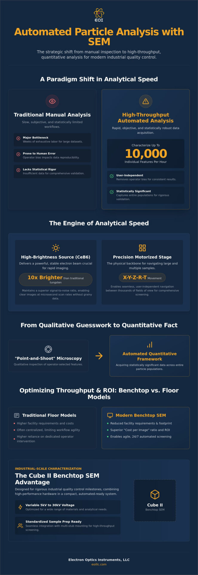
Did you know that modern analytical systems are now capable of characterizing up to 10,000 individual features per hour, a feat that would take a manual operator weeks of exhaustive labor? The transition toward high-throughput automated particle analysis sem represents a fundamental transformation in industrial quality control, where the necessity for precision intersects with the demand for unprecedented scale. You’ve likely experienced the frustration of manual feature detection, which remains inherently prone to human error; these bottlenecks often result in data sets that lack the statistical rigor required for high-stakes manufacturing and material validation.
It’s clear that traditional microscopy workflows are often too slow to meet the relentless demands of modern, 24/7 production environments. This article explores the technical requirements and strategic advantages of automated SEM for rapid, statistically significant particle characterization within the 2026 industrial environment. We’ll examine how the integration of high-brightness sources and sophisticated motorization in benchtop systems like the Cube II facilitates user-independent screening, exploring how these advancements reduce labor costs while significantly improving time-to-data for critical quality milestones.
Key Takeaways
- Identify the synergy between high-brightness CeB6 sources and motorized X-Y-Z-R-T stages that enables rapid signal acquisition without sacrificing the meticulous detail required for material validation.
- Transition from qualitative “point-and-shoot” microscopy to a quantitative framework using automated particle analysis sem to capture statistically significant data across expansive particle populations.
- Assess the logistical and financial advantages of benchtop SEM systems, focusing on reduced facility requirements and a superior “Cost per Image” ratio compared to traditional floor models.
- Implement standardized sample preparation protocols, such as multi-stub mounting and optimized conductive coating, to ensure seamless navigation during high-throughput screening cycles.
- Explore the technical specifications of the Cube II Benchtop SEM, including its variable 5kV to 30kV voltage range, designed for rigorous industrial quality control milestones.
The Paradigm Shift to Automated Particle Analysis SEM
The modern industrial sector requires more than just high-resolution imagery; it demands actionable, statistically robust data sets. This requirement has catalyzed the primary adoption of automated particle analysis sem, a process defined by the user-independent acquisition of morphological and chemical data across expansive particle populations. Traditional microscopy often relies on a “point-and-shoot” methodology, where an operator manually selects features of interest. While this approach is sufficient for basic defect inspection, it fails to meet the rigorous quantitative requirements of contemporary materials science. Modern production cycles for additive manufacturing powders, battery electrode materials, and semiconductor components necessitate a comprehensive understanding of entire populations, not just isolated examples.
At its core, the Scanning electron microscope (SEM) serves as the foundational hardware for these workflows, but the shift toward automation transforms the instrument from a qualitative tool into a high-throughput diagnostic engine. Achieving statistical significance in particle size distribution (PSD) and shape analysis is no longer optional. For industries like aerospace or energy storage, a single outlier in a powder batch can lead to catastrophic mechanical failure or thermal runaway. Automation ensures that every particle is accounted for, providing the empirical foundation needed for rigorous material validation.
The Evolution of Analytical Speed
Analytical speed has undergone a dramatic trajectory, moving away from centralized, manual floor models toward agile, high-performance desktop SEM systems. This evolution reflects a growing market demand for 24/7 automated screening within high-tech manufacturing environments. In these settings, manual operator intervention isn’t just a cost center; it’s the primary bottleneck that limits characterization workflows and introduces subjective bias into critical quality control data. By removing the human element from the primary detection loop, laboratories can achieve a steady, predictable flow of information that matches the pace of modern production lines.
Defining Key Performance Indicators (KPIs) for Screening
Establishing Key Performance Indicators (KPIs) is essential for optimizing automated particle analysis sem protocols. There’s an inherent trade-off between spatial resolution and throughput speed, as higher magnification typically requires longer dwell times. We define “analytical throughput” as the total volume of valid data points generated per hour, a metric that prioritizes statistical relevance over individual image aesthetics. Automated software plays a vital role here, ensuring that data remains reproducible across different shifts and operators. This consistency is vital for maintaining the integrity of global supply chains and ensuring that quality milestones are met without fail.
Hardware and Software Synergy: The Engine of Analytical Speed
The efficacy of automated particle analysis sem depends on a symbiotic relationship between hardware architecture and software logic. At the heart of this synergy is the electron source. High-brightness sources, such as Cerium Hexaboride (CeB6) filaments, provide up to ten times the brightness of traditional tungsten cathodes. This increased brightness is critical during high-speed scanning because it maintains a superior signal-to-noise ratio, allowing the system to capture clear images at dwell times that would otherwise result in unusable, grainy data. When the objective is to characterize thousands of particles in a single session, the ability to maintain image integrity at microsecond scan rates is a non-negotiable requirement for industrial laboratories.
Precision stage movement serves as the physical backbone of high-throughput characterization. High-precision motorized X-Y-Z-R-T stages are necessary for seamless multi-sample navigation, enabling the system to move between discrete fields of view with sub-micron repeatability. A significant challenge in automated workflows is maintaining vacuum stability during these rapid, aggressive stage movements. Industrial-grade systems address this by utilizing robust vacuum management protocols that prevent pressure fluctuations from degrading beam stability. These hardware advancements are increasingly augmented by advanced, AI-driven methods that optimize feature extraction in real-time, ensuring that the software can distinguish between overlapping particles or complex textures without human intervention.
Detection systems must also be optimized for speed. Backscattered electron (BSE) detectors are the primary tool for particle detection because they provide rapid compositional contrast based on atomic number (Z-contrast). This allows the software to instantly differentiate high-density particles from a low-density substrate. By integrating high-count-rate EDS detectors, researchers can achieve “on-the-fly” chemical characterization. If you’re looking to upgrade your laboratory’s capabilities, exploring a Veritas Series SEM provides the necessary hardware foundation for these demanding automated protocols.
Automated Image Acquisition Protocols
To analyze large-area samples without sacrificing detail, systems employ “tiling and stitching” techniques that create high-resolution composite maps from hundreds of individual image frames. Maintaining quality during these long, unattended runs requires sophisticated automated focus and stigmation algorithms that compensate for sample tilt or height variations in real-time. The maximum achievable scan rate is ultimately governed by detector bandwidth; wider bandwidths allow the electronics to process signals faster, directly increasing the number of particles characterized per hour.
Energy Dispersive Spectroscopy (EDS) Integration
Modern high-throughput environments rely on Silicon Drift Detector (SDD) technology, which handles significantly higher X-ray count rates than older detector generations. This allows EDS analysis to be synchronized directly with the electron beam for rapid elemental mapping. Beam current stability is the primary determinant of EDS data accuracy during extended automated screening sessions, as any drift can lead to inconsistent elemental quantification across the sample set. This precision ensures that every data point contributes to a reliable, statistically significant representation of the particle population.
Benchtop vs. Floor Models: Optimizing Throughput and ROI
Choosing between benchtop and floor-model architectures is a critical strategic decision that influences both immediate operational efficiency and long-term return on investment. While floor-model systems are often perceived as the gold standard for versatility, they impose significant facility requirements, including dedicated plumbing for water cooling, advanced vibration isolation platforms, and specialized high-power electrical circuits. In contrast, benchtop systems eliminate these logistical hurdles, allowing for rapid deployment in existing quality control environments. When analyzing the “Cost per Image” metric, organizations must factor in not only the initial capital expenditure but also the ongoing operational labor required to maintain complex systems. For roughly 90% of routine industrial tasks involving automated particle analysis sem, the Cube II Benchtop SEM provides an optimized balance of performance and cost-efficiency, challenging the traditional reliance on larger, more expensive hardware.
There’s a persistent misconception that higher accelerating voltages, typically associated with floor models, are always superior for screening applications. In reality, excessive voltage can often lead to deleterious charging effects on non-conductive particles or obscure critical surface morphologies due to deeper electron penetration. Modern benchtop systems offer the precision necessary to achieve high-quality data without the overhead of a centralized microscopy facility. By prioritizing the specific resolution requirements of the application over raw voltage capacity, labs can achieve a higher throughput of valid data points while significantly reducing their total cost of ownership.
Logistical Advantages of Benchtop Systems
Benchtop systems provide distinct logistical advantages that directly impact daily throughput. The Cube II, for example, features a vacuum readiness time of approximately 90 seconds, allowing for frequent sample changes that would be impossible with larger, high-volume chambers. This rapid cycle time is complemented by a simplified loading process and an intuitive interface that reduces the training curve for non-expert personnel. In space-constrained industrial laboratories, the compact footprint of a benchtop system enables the integration of high-end characterization directly onto the production floor, facilitating real-time decision-making.
High-Resolution Alternatives for Complex Samples
For specialized applications requiring the detection of features at the sub-nanometer scale, laboratories may need to consider advanced SEM techniques. The Veritas Series FE-SEM utilizes a field emission source to provide the extreme brightness and beam stability necessary for high-resolution automated particle analysis sem. While thermionic sources are ideal for high-throughput screening of micron-scale particles, the Veritas Series FE-SEM is required when compositional mapping must be performed at the limits of modern microscopy, ensuring that even the most complex samples are characterized with absolute accuracy and stability over long, unattended acquisition sessions.
Strategic Implementation: Transitioning to Automated Workflows
Integrating automated particle analysis sem into a laboratory’s standard operating procedure requires a systemic overhaul of both hardware utilization and sample preparation logic. The transition begins with the adoption of high-density multi-stub holders, which facilitate the sequential characterization of numerous specimens without the need for frequent vacuum cycles. Precise conductive coating techniques, such as automated sputter coating with gold or carbon, are equally vital; non-uniformity in the conductive layer can induce localized charging, which inevitably disrupts the automated feature detection algorithms during extended, unattended screening sessions. By standardizing these initial steps, a facility can ensure that the transition from manual to automated workflows is both seamless and technically sound.
Establishing a clear framework for return on investment (ROI) involves a meticulous comparison between manual labor costs and the accelerated throughput of automated systems. When an expert microscopist is relieved from the repetitive burden of manual feature counting, they can refocus their expertise on high-level data interpretation and strategic process optimization. The cost of the system is typically amortized through the elimination of human-induced variability and the ability to process a significantly higher volume of samples within the same operational window. This shift in labor allocation not only reduces the cost-per-sample but also accelerates the timeline for critical quality control milestones.
Operating a system at a high duty cycle necessitates a disciplined approach to technical upkeep. Adhering to a structured SEM maintenance schedule is the only way to ensure that vacuum integrity and beam stability remain within the tight tolerances required for high-throughput screening. Without regular intervention, the accumulation of contaminants within the column can degrade the signal-to-noise ratio, eventually compromising the accuracy of the automated data.
Maximizing System Uptime and Reliability
Unplanned downtime is the primary threat to productivity in a high-tech manufacturing environment. Implementing annual service contracts provides a proactive layer of security, ensuring that critical components are replaced before they reach their failure threshold. On-site technical training is another essential pillar of reliability, as it ensures that the internal staff can effectively manage the nuances of automated data acquisition. EOI’s comprehensive service capability extends across all major SEM manufacturers, providing a single point of technical authority to maintain lab-wide operational stability. To protect your laboratory’s output, you should book a preventative maintenance visit to ensure your hardware remains optimized for 24/7 operation.
Data Management and AI Feature Recognition
The sheer volume of information generated by automated screening protocols presents a significant data management challenge. AI-driven software suites provide the solution by facilitating automated feature recognition, classification, and the generation of standardized reports. This technological integration removes the risk of subjective operator bias and allows for the immediate identification of quality deviations. By 2026, machine learning will be the primary driver in streamlining SEM data interpretation by autonomously filtering and prioritizing critical features within massive particle populations.
The Cube II Advantage: Industrial-Scale Particle Characterization
The Cube II Benchtop SEM stands as the premier high-throughput solution for organizations seeking to internalize their characterization workflows without the logistical burden of a centralized microscopy suite. This platform is engineered specifically for the rigors of automated particle analysis sem, offering a variable accelerating voltage range from 5kV to 30kV. Such versatility is essential for industrial quality control, as it allows operators to tune the electron beam for surface-sensitive imaging of light polymers or high-penetration analysis of dense metallic inclusions. The robust motorized stage system provides the physical stability required for long-duration screening, ensuring that the coordinate accuracy remains consistent across thousands of discrete fields of view. By integrating these high-end specifications into a portable, 70kg architecture, the Cube II facilitates a decentralized approach to material validation where precision is maintained at the point of production.
Establishing complex automated screening protocols shouldn’t require a doctorate in electron optics. The Cube II features a user-friendly interface designed for rapid setup, allowing technicians to define scan areas and classification parameters with minimal training. This accessibility ensures that the transition to user-independent data acquisition is immediate, providing a reliable stream of quantitative data to guide manufacturing adjustments. Partnering with Electron Optics Instruments, LLC for the implementation of these systems ensures long-term analytical excellence, as our technical authority is backed by decades of experience in specialized industrial sectors and a commitment to meticulous hardware integration.
Cube II Performance for High-Volume Labs
In high-volume environments, the technical specifications of the Cube II provide a distinct competitive edge. The system achieves a magnification range of up to 200,000x, allowing for the detection of fine surface morphologies that are often invisible to entry-level analyzers. Its robust vacuum architecture is a hallmark of the design, featuring a 90-second vacuum readiness time that minimizes downtime during high-frequency sample cycling. When paired with advanced EDS systems, the Cube II delivers total material characterization, providing both the morphological and elemental data necessary for comprehensive particle populations. This synergy between rapid vacuum recovery and high-speed detection makes the platform ideal for 24/7 industrial screening.
National Service and Expert Support
Reliability in automated particle analysis sem depends as much on the supporting infrastructure as it does on the primary hardware. Electron Optics Instruments, LLC maintains a comprehensive national field service network, providing expert technical support across all major SEM brands to ensure your laboratory maintains peak operational stability. For organizations looking to expand their analytical capacity while managing capital expenditure, exploring our inventory of refurbished SEM units offers a cost-effective pathway to industrial-scale characterization. If you’re ready to transform your quality control milestones through high-throughput automation, contact Electron Optics Instruments, LLC for a Cube II technical demonstration today.
Advancing Industrial Precision through Automated Characterization
The integration of automated particle analysis sem into the industrial quality control framework marks a definitive departure from subjective, manual microscopy. By leveraging high-brightness sources and motorized stage precision, modern laboratories can now achieve the statistical robustness required for 2026’s rigorous production standards. This evolution ensures that critical quality milestones are reached with unprecedented speed, allowing for the characterization of massive particle populations without the logistical overhead of traditional centralized facilities. The transition toward user-independent screening represents a fundamental pillar of modern manufacturing excellence.
Electron Optics Instruments remains at the forefront of this technological shift, providing over 30 years of specialized expertise in electron microscopy. As the sole US distributor for EmCraft Scanning Electron Microscopes and a provider of comprehensive service and repair for all major SEM manufacturers, we’re uniquely positioned to support your laboratory’s transformation. We invite you to Request a Technical Consultation for Your Automated SEM Workflow to optimize your characterization protocols. Your path to industrial-scale precision begins with a partner dedicated to technical reliability and international excellence.
Frequently Asked Questions
What is the primary difference between high-throughput SEM and standard SEM?
The primary distinction lies in the transition from qualitative, operator-dependent observation to quantitative, user-independent data acquisition. Standard SEM relies on a “point-and-shoot” methodology where a microscopist manually selects features. In contrast, automated particle analysis sem utilizes motorized stages and advanced software to systematically scan expansive areas, characterizing thousands of features per hour without human bias or fatigue. This shift transforms the instrument into a high-speed diagnostic engine for industrial validation.
How does automation improve the statistical accuracy of particle analysis?
Automation enhances statistical accuracy by facilitating the characterization of significantly larger populations, moving beyond the anecdotal evidence provided by manual selection. By analyzing thousands of individual particles rather than a small, subjective subset, laboratories can achieve a rigorous particle size distribution (PSD) that reflects the true nature of the material batch. This empirical approach is vital for identifying rare outliers or contaminants that would likely be overlooked during traditional manual screening protocols.
Can benchtop SEM systems handle industrial-scale high-throughput workloads?
Benchtop SEM systems are increasingly engineered to sustain industrial-scale high-throughput workloads, often outperforming floor models in routine screening efficiency. Platforms like the Cube II feature robust vacuum architectures and high-precision motorized stages specifically designed for the rapid cycling required in 24/7 production environments. While floor models offer extreme versatility, benchtop systems provide a more optimized “Cost per Image” for the vast majority of standardized industrial particle characterization tasks.
What industries benefit the most from automated SEM screening?
Industries requiring meticulous material validation, such as additive manufacturing, battery technology, and semiconductor fabrication, derive the most significant benefits from these systems. In additive manufacturing, the morphology and cleanliness of metal powders directly influence the structural integrity of the final component. Similarly, battery manufacturers utilize automated screening to ensure electrode uniformity and detect metallic impurities that could compromise safety, making high-throughput characterization an essential pillar of their quality control framework.
How often does an automated SEM system require preventative maintenance?
An automated SEM system running at a high duty cycle typically requires a comprehensive preventative maintenance visit at least once per year to ensure vacuum integrity and beam stability. Systems operating in 24/7 production environments may benefit from semi-annual inspections to prevent the accumulation of contaminants within the column. Adhering to a structured maintenance schedule is necessary to maintain the tight tolerances required for reproducible automated particle analysis sem results over long-term operations.
Does high-throughput screening compromise the resolution of the SEM images?
High-throughput screening doesn’t inherently compromise resolution, although there’s a practical trade-off between scan speed and image aesthetics. By utilizing high-brightness sources like CeB6 filaments, systems maintain a superior signal-to-noise ratio even at microsecond dwell times. This allows the hardware to capture the necessary morphological data for accurate classification without the significant time investment required for ultra-high-resolution imaging, prioritizing statistical relevance and analytical throughput for industrial milestones.
What are the specific sample preparation requirements for automated SEM analysis?
Automated workflows require standardized preparation, primarily focusing on the use of multi-stub holders and uniform conductive coating. Utilizing high-density holders allows for the sequential analysis of multiple specimens without breaking vacuum, significantly increasing throughput. Furthermore, automated sputter coating ensures a consistent conductive layer across all samples, which is vital for preventing localized charging that would otherwise disrupt the software’s feature recognition and classification algorithms during unattended runs.
Is AI integration necessary for managing high-throughput SEM data?
AI integration is essential for managing the massive data sets generated by modern high-throughput screening protocols. As systems generate thousands of data points per hour, manual interpretation becomes a logistical impossibility. AI-driven software facilitates automated feature recognition and classification, transforming raw imagery into actionable reports. By 2026, machine learning will be the primary mechanism for streamlining data interpretation, allowing for real-time identification of quality deviations across global supply chains.