
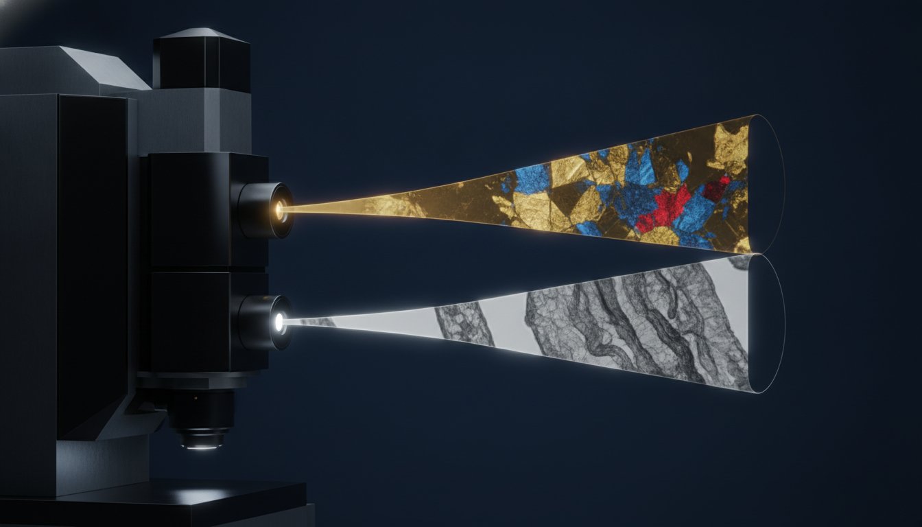
The integrity of analytical data in scanning electron microscopy is fundamentally tethered to the spatial and energetic sensitivity of the detection system employed. A failure to align detector geometry with specific material properties often results in the irreparable loss of critical surface morphology or the conflation of topographical and compositional signals. Consequently, choosing the right sem detector has evolved into a multidimensional optimization challenge that demands a rigorous understanding of secondary and backscattered electron trajectories.
We recognize the persistent technical frustrations associated with insufficient contrast in complex multi-phase materials and the degradation of surface detail under high accelerating voltages. This technical guide provides the framework necessary to master the nuances of electron detection, ensuring you can optimize image contrast, compositional accuracy, and laboratory throughput. We’ll examine how to select an SEM system, such as the Veritas Series or the CUBE-II benchtop, that balances high-resolution requirements with analytical versatility while significantly reducing imaging artifacts and optimizing EDS integration. By prioritizing meticulous detector selection, you ensure that your laboratory’s hardware aligns with the grounded, practical realities of high-end industrial production and logistical excellence.
Key Takeaways
- Learn to differentiate between secondary and backscattered electron signals to effectively isolate intricate topographical features from subsurface compositional information.
- Refine the technical process of choosing the right sem detector by systematically evaluating the spatial constraints of the chamber alongside the resolution benefits of in-column configurations.
- Address the interaction volume challenge by aligning accelerating voltages with material density to maintain high-resolution clarity and prevent artifacts on non-conductive samples.
- Facilitate superior laboratory outcomes by integrating EDS systems that complement detector performance for concurrent structural and chemical analysis.
- Assess the scalability of your analytical capabilities by determining when to transition from a high-throughput Cube II Benchtop SEM to the advanced architectural versatility of the Veritas Series.
The Fundamentals of Electron Detection: Secondary vs. Backscattered Signals
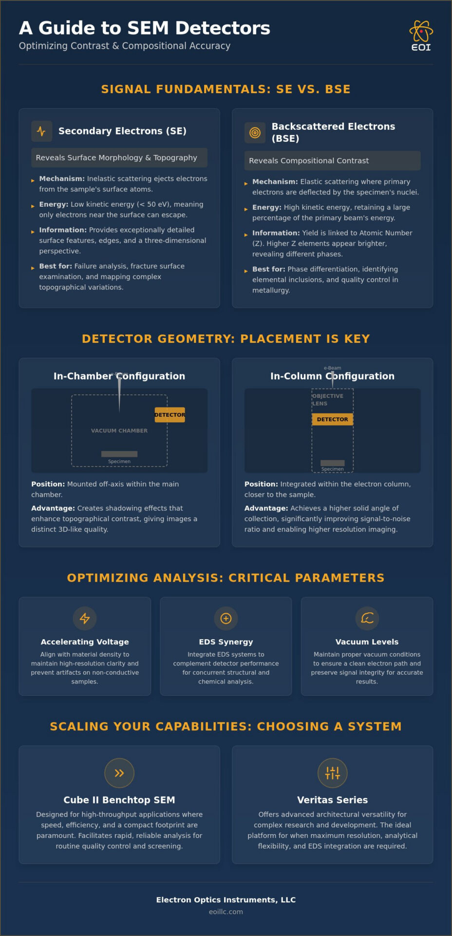
The precision of a Scanning Electron Microscope (SEM) is fundamentally derived from the interaction between the primary electron beam and the specimen’s atomic lattice. These interactions yield a diverse spectrum of signals, primarily categorized as secondary electrons (SE) and backscattered electrons (BSE). Distinguishing between these two signals is the first step in choosing the right sem detector, as their kinetic energies and origins dictate the depth and type of information retrieved. Secondary electrons are the product of inelastic scattering, where the primary beam transfers energy to the specimen’s electrons, ejecting them with low kinetic energy, typically less than 50 eV. Because of this low energy, only those electrons generated near the surface can escape, making SE signals exceptionally sensitive to surface morphology.
Backscattered electrons result from elastic scattering events, where the primary electrons are deflected by the specimen’s nuclei. These electrons retain a high percentage of their original kinetic energy and originate from deeper within the interaction volume. The yield of backscattered electrons is intrinsically linked to the atomic number (Z) of the material. Choosing the right sem detector requires a meticulous evaluation of these scattering events to ensure the collected data aligns with the analytical objective. If the research goal is to map complex topographical variations, SE detection is paramount. Conversely, if the objective is to distinguish between different phases or identify elemental inclusions, BSE detection provides the necessary compositional depth.
Secondary Electron Detectors (SED) for Surface Morphology
The Everhart-Thornley detector remains the industry standard for capturing low-energy secondary electrons. It utilizes a scintillator and a photomultiplier tube to convert electron strikes into light and then back into an electrical signal. A bias voltage applied to a collector screen, or Faraday cage, creates an electrostatic field that draws in low-energy electrons from various angles. This setup is critical for failure analysis and fracture surface examination, as it highlights edges and provides a three-dimensional perspective of the sample. Adjusting the bias voltage directly influences collection efficiency, allowing operators to enhance image brightness and contrast in shadowed regions of a specimen.
Backscattered Electron Detectors (BSD) for Phase Differentiation
Solid-state backscattered electron detectors are engineered to identify subtle compositional variations within alloys, polymers, and geological samples. These detectors are typically positioned directly above the sample to maximize the collection of high-energy electrons reflecting back toward the column. They are indispensable for identifying contaminants or inclusions that may be invisible in a standard topographical scan. Atomic number contrast represents the direct correlation between the backscattering coefficient and the mean atomic number of the sample, where regions of higher Z appear brighter due to increased electron deflection. This capability allows for the rapid identification of heavy-element precipitates within a lighter matrix, ensuring rigorous quality control in metallurgical applications.
Detector Geometry and Placement: In-Chamber vs. In-Column Configurations
The spatial architecture of the vacuum chamber serves as a critical determinant in the fidelity of electron collection. When choosing the right sem detector, the physical distance between the specimen and the detector face dictates the solid angle of signal acquisition, which directly impacts the signal-to-noise ratio. Detectors mounted within the chamber are traditionally positioned at an off-axis angle relative to the primary beam. This geometry introduces a directional bias that enhances topographical contrast through shadowing effects, yet it may also result in information loss within deep trenches or high-aspect-ratio features. The proximity of the detector to the pole piece is a fundamental variable that determines whether the resulting image prioritizes broad-field morphology or extreme surface detail.
In-Chamber Detectors: Versatility for Industrial QC
Standard chamber-mounted detectors provide the operational flexibility required for diverse industrial applications. Systems like the Cube II Benchtop SEM leverage optimized chamber geometry to facilitate rapid sample screening, allowing for the analysis of large specimens that require significant stage tilt. This versatility is essential when examining non-conductive materials or performing failure analysis on bulky components where a short working distance is impractical. By maintaining a respectful distance from the pole piece, these detectors ensure that the system remains robust against accidental collisions while providing sufficient contrast for routine inspections. For those seeking to refine their laboratory throughput, exploring the specialized hardware configurations offered by EOI can streamline this selection process.
In-Column and Through-the-Lens (TTL) Detection
Achieving nanometer-scale precision requires a departure from traditional chamber-mounted geometries. In-column detectors (ICD) and through-the-lens (TTL) systems, such as those integrated into the Veritas HR and Veritas FE SEM models, utilize the electromagnetic field of the objective lens to guide electrons toward the detector. This mechanism effectively filters out “noise” generated by electrons that have reflected off the chamber walls, focusing exclusively on signals originating from the beam-specimen interaction point. Fundamental SEM Detector Imaging Principles dictate that as the working distance decreases, the efficiency of TTL detection increases, allowing for ultra-high-resolution imaging that preserves the integrity of the specimen’s finest surface details. This configuration is particularly advantageous for semiconductor inspection and advanced nanomaterial characterization where every angstrom of detail is vital for analytical precision.
Application-Driven Selection: Mapping Detectors to Material Science Challenges
The efficacy of material characterization is contingent upon a strategic approach to instrument configuration. Choosing the right sem detector involves more than just selecting for resolution; it requires a rigorous assessment of how the specimen interacts with the electron beam under varying vacuum conditions. For researchers engaged in advanced sem techniques, the selection process is a balancing act between signal intensity and the specific data required for structural or chemical validation. Biological samples, for example, often require low-vacuum environments to prevent dehydration and charging, which necessitates specialized detectors that can function effectively in the presence of residual gas molecules. The selection matrix for these systems is often defined by the scale of the investigation; while a benchtop unit like the Cube II provides the requisite speed for process control, a field-emission system like the Veritas FE is mandatory for sub-nanometer defect review. It’s this level of meticulousness that distinguishes a reliable partner in the industrial sector.
Semiconductor and Electronics Failure Analysis
Failure analysis within the electronics industry demands the isolation of sub-micron defects that could compromise device integrity. Secondary electron detectors are indispensable for identifying metallization defects and cracks that manifest as minute topographical variations. In deep-trench architectures, the phenomenon of voltage shadowing becomes a critical tool; it allows the detector to reveal hidden geometries that standard imaging might obscure. Integrating EDS (Energy Dispersive Spectroscopy) systems alongside these detectors enables the simultaneous identification of elemental contaminants, transforming a simple visual inspection into a comprehensive forensic analysis of the wafer. This synergy is vital for maintaining the rigorous quality standards required in high-volume semiconductor manufacturing where precision is non-negotiable.
Metallurgy and Geological Characterization
In metallurgy and geology, the primary challenge lies in distinguishing between phases that possess similar physical densities but distinct chemical compositions. Multi-segment backscattered electron detectors (BSD) address this by providing a nuanced view of the specimen’s internal structure. These detectors are particularly effective for grain boundary visualization in complex alloys, where the orientation of individual grains influences the backscattering coefficient. By utilizing the topographic (TOPO) mode in solid-state detectors, operators can enhance surface contrast without sacrificing the compositional data inherent in the backscattered signal. Quadrant-based BSDs facilitate the mathematical separation of topographic and compositional data by comparing the signals collected from different detector segments. This differentiation is essential for identifying inclusions and precipitates that dictate the mechanical properties of industrial materials, ensuring that every batch meets the necessary specifications for international production. When choosing the right sem detector for these environments, the ability to isolate these variables determines the reliability of the final analytical report.
Critical Parameters: Accelerating Voltage, Vacuum Levels, and EDS Synergy
The analytical precision of an electron microscope is intimately linked to the management of the interaction volume, a three-dimensional region within the specimen where the primary beam dissipates its energy. Accelerating voltage serves as the primary lever for controlling this volume; while higher voltages facilitate deeper penetration for subsurface imaging, they often obscure the fine morphological details of the surface. Choosing the right sem detector necessitates a strategic alignment with these voltage parameters to ensure that the resulting signal remains representative of the area of interest. In variable pressure or environmental SEM modes, the presence of gas molecules introduces additional scattering events, requiring detectors with high collection efficiency to maintain image stability. This meticulous calibration ensures that the laboratory’s output remains consistent with the highest standards of international production and research excellence.
Low-Voltage Imaging and Charge Compensation
Imaging beam-sensitive materials, such as polymers or advanced composites, requires a significant reduction in accelerating voltage to prevent structural degradation and specimen charging. High-sensitivity detectors integrated into the Veritas Pro series are specifically engineered to operate at low beam currents, preserving the sample’s architectural integrity while providing sufficient signal-to-noise ratios. When choosing the right sem detector for these applications, the efficiency of the sensor becomes the primary bottleneck for achieving nanometer-scale resolution. By utilizing these advanced detection systems, researchers can image non-conductive samples without the need for traditional sputter coating, which can often mask the very sub-micron features under investigation. This capability is vital for industries focused on sustainable development and advanced material synthesis, where the true state of the specimen must be documented without artificial modification.
EDS Integration and Geometric Interference
Achieving a holistic understanding of a specimen requires the seamless synergy between electron detection and Energy Dispersive Spectroscopy (EDS). A common oversight in instrument configuration is the geometric interference between the electron detector hardware and the EDS detector’s line-of-sight. If the electron detector is improperly positioned, it can obstruct the X-rays emitted from the sample, leading to inaccurate quantitative elemental analysis. Take-off angles must be meticulously optimized to ensure that X-rays reach the EDS sensor without shadowing from the specimen’s topography or the microscope’s internal components. Optimizing the working distance for simultaneous imaging and EDS mapping allows for a more efficient workflow, reducing the time required for comprehensive sample characterization. To enhance your laboratory’s analytical depth, you can explore our range of EDS (Energy Dispersive Spectroscopy) Systems that are designed to integrate flawlessly with the Veritas and Cube II series.
Strategic Procurement: Optimizing Your Laboratory Workflow with the Veritas and Cube II Series
Strategic procurement in the analytical sector requires a forward-looking perspective that balances immediate laboratory throughput with long-term technological scalability. Choosing the right sem detector is a capital investment decision that dictates the quality of institutional data for years to come. For high-throughput industrial environments, the Cube II Benchtop SEM offers an exceptional cost-to-performance ratio, providing reliable secondary electron imaging for rapid sample screening without the spatial requirements of a floor-standing unit. This system allows for the decentralization of routine inspections, freeing up advanced instrumentation for more complex tasks. As laboratory requirements evolve toward more intricate nanotechnology and sub-micron characterization, transitioning from the Genesis Tabletop to the Veritas Series ensures that the detection hardware keeps pace with increasing analytical demands.
Selecting the Right SEM Model for Your Budget
Selecting the optimal model involves a meticulous assessment of specific research objectives and fiscal realities. The Veritas HR, optimized for high-resolution topographical mapping, serves as a cornerstone for materials science labs, while the Veritas FE utilizing field-emission technology provides the extreme precision necessary for semiconductor inspection and advanced wafer review. For laboratories seeking high-end analytical capabilities while managing stricter capital constraints, refurbished SEM units represent a sophisticated value proposition, offering access to advanced detector arrays at a significantly lower entry point. Engaging with specialists to define custom detector configurations ensures that the hardware is precisely tuned to the unique requirements of your industrial sector, preventing the unnecessary expense of redundant features while maximizing relevant data acquisition.
Longevity Through Service and Preventive Maintenance
The sensitivity of advanced electron detectors is a perishable asset that requires rigorous protection against the harsh realities of vacuum operation. Implementing a proactive strategy for sem maintenance is essential for preserving the integrity of the detector’s electronics and preventing vacuum contamination that can degrade signal quality over time. Regular calibration protocols are necessary to maintain consistent Z-contrast and spatial resolution, ensuring that data collected today remains comparable to future benchmarks. Adhering to professional standards for sem operation ensures that daily management practices contribute to the longevity of the sensor and the overall stability of the electron column. Leveraging on-site training and professional field service allows your team to maximize equipment utility, transforming a sophisticated instrument into a reliable pillar of institutional progress and international logistical excellence.
Advancing Analytical Precision through Meticulous Configuration
The evolution of electron microscopy in 2026 demands a sophisticated approach to hardware integration where every parameter, from electron trajectory to vacuum stability, is optimized for the specimen at hand. Choosing the right sem detector is no longer a peripheral concern but a foundational requirement for laboratories that prioritize compositional accuracy and high-throughput reliability. By aligning detector geometry with specific material science challenges and ensuring seamless synergy with EDS systems, your facility can effectively eliminate common imaging artifacts while preserving the finest surface details.
As the exclusive US distributor for EmCraft SEMs and a partner with over 30 years of electron microscopy expertise, we provide the technical depth necessary to refine your laboratory’s capabilities. Our commitment to meticulousness extends from initial procurement to long-term support through comprehensive service contracts for all major SEM brands. Consult with our technical experts to configure your Veritas or Cube II SEM system to ensure your hardware remains a reliable pillar of industrial innovation. we look forward to supporting your pursuit of superior standards and analytical excellence.
Frequently Asked Questions
How do I decide between an Everhart-Thornley and a solid-state detector?
Your decision depends on whether you prioritize topographical mapping or compositional contrast. Everhart-Thornley detectors are engineered to capture low-energy secondary electrons, making them ideal for high-resolution surface morphology. Solid-state detectors are generally optimized for backscattered electrons, providing the atomic number contrast necessary to distinguish between different phases in a specimen. Choosing the right sem detector for your workflow requires aligning these sensor capabilities with your primary analytical objectives.
Can I add a backscattered electron detector to an existing benchtop SEM?
Retrofitting a backscattered electron detector to an existing benchtop system is contingent upon the instrument’s chamber architecture and available vacuum ports. While many modern systems are designed for modularity, some compact units have fixed detector configurations to maintain their small footprint. It’s essential to verify the hardware compatibility of your specific model with the manufacturer to ensure that the integration doesn’t compromise the system’s vacuum integrity or spatial resolution.
What is the impact of a high accelerating voltage on secondary electron imaging?
High accelerating voltages increase the interaction volume within the specimen, which often results in the degradation of fine surface detail. As the primary beam penetrates deeper, the secondary electrons generated from the subsurface can obscure the topographical information from the outermost layers. This phenomenon, often referred to as the edge effect, can lead to artificial brightness that complicates the interpretation of sub-micron morphological features during failure analysis.
Is a 4-quadrant BSD necessary for routine metallurgical analysis?
A 4-quadrant backscattered electron detector is highly advantageous for routine metallurgical analysis because it allows for the mathematical separation of topographic and compositional data. By comparing the signals from different segments, operators can isolate grain boundary morphology from the atomic number contrast of the matrix. This capability ensures a more comprehensive understanding of the alloy’s microstructure, which is vital for maintaining the rigorous quality standards required in international industrial production.
How does the working distance affect the collection efficiency of in-chamber detectors?
Working distance directly dictates the solid angle of electron collection for in-chamber detectors. Reducing the distance between the pole piece and the specimen generally increases the collection efficiency for backscattered electrons, resulting in a higher signal-to-noise ratio. However, an excessively short working distance can introduce shadowing effects or physical obstructions that limit the trajectory of secondary electrons toward the Everhart-Thornley detector, potentially compromising the clarity of topographical images.
What are the signs that an SEM detector is failing or needs service?
Primary indicators of detector degradation include a persistent increase in image noise, the appearance of streaks, or a significant loss of brightness that cannot be corrected through standard alignment. For scintillator-based detectors, a decline in sensitivity often suggests that the phosphor coating has reached the end of its operational lifespan. Regular preventative maintenance visits are essential to identify these subtle performance shifts before they lead to catastrophic failure or the corruption of critical analytical data.
Why is detector geometry critical for EDS analysis?
Detector geometry is critical for Energy Dispersive Spectroscopy because the X-ray signal requires an unobstructed line-of-sight from the specimen to the EDS sensor. Choosing the right sem detector involves ensuring that the electron detection hardware doesn’t physically shadow the X-ray detector at the optimal working distance. Improper geometry can lead to reduced count rates and inaccurate quantitative results, particularly when analyzing specimens with complex topographical features or high-aspect-ratio structures.
Does the Cube II Benchtop SEM support both SE and BSE detection simultaneously?
The Cube II Benchtop SEM is engineered to support simultaneous secondary and backscattered electron detection, providing a holistic view of the sample’s surface and composition in a single scan. This dual-detection capability is essential for high-throughput environments where rapid screening and precise phase identification are required. By integrating these signals, the system allows researchers to correlate topographical features with elemental variations, ensuring meticulousness in both routine quality control and specialized industrial research.