

Could that anomalous surface protrusion actually be a deceptive instrumental ghost rather than a breakthrough discovery? In the rigorous domain of electron microscopy, the distinction between a critical sample feature and a misleading aberration often determines the ultimate success of an entire research initiative. You likely understand the profound frustration of losing hours to recalibration or, even worse, mischaracterizing a specimen due to common sem image artifacts that obscure the underlying truth of your materials.
This 2026 diagnostic guide provides a comprehensive technical framework to identify and mitigate these distortions, ensuring your Veritas series or Cube II instrumentation delivers the crisp, high-resolution data your laboratory demands. We’ll examine the technical origins of charging, astigmatism, and environmental interference while offering actionable protocols to streamline your imaging workflows, minimize instrument downtime, and maximize the ROI of your analytical systems. By mastering these diagnostic procedures, you’ll transform your microscopy from a source of uncertainty into a pillar of institutional reliability and technical excellence.
Key Takeaways
- Learn to distinguish between authentic specimen topography and non-representative features by categorizing the tripartite origins of common sem image artifacts.
- Identify the specific visual signatures of electrostatic charging and astigmatism to prevent the mischaracterization of materials during high-stakes research.
- Develop a diagnostic workflow for detecting environmental interference, including mechanical vibration and electromagnetic fields that compromise resolution.
- Evaluate how modern SEM platforms like the Cube II and Veritas series utilize automated mitigation strategies to ensure consistent image clarity.
- Recognize the role of professional preventative maintenance and precise installation in securing the highest possible ROI for your laboratory’s analytical capabilities.
Understanding the Taxonomy of Artifacts in Scanning Electron Microscopy
In the pursuit of nanometric precision, the integrity of visual data is paramount. An artifact represents any feature within a micrograph that doesn’t correspond to the physical reality of the specimen being analyzed. Distinguishing these non-representative features from true sample topography is a foundational requirement for any researcher. Failure to do so often results in the mischaracterization of materials, which carries a significant economic burden in high-stakes environments. Within the context of industrial failure analysis, the misinterpretation of common sem image artifacts can lead to erroneous conclusions regarding component fatigue or manufacturing defects. This oversight frequently triggers costly false positives in quality control protocols, potentially halting production lines or necessitating unnecessary re-engineering.
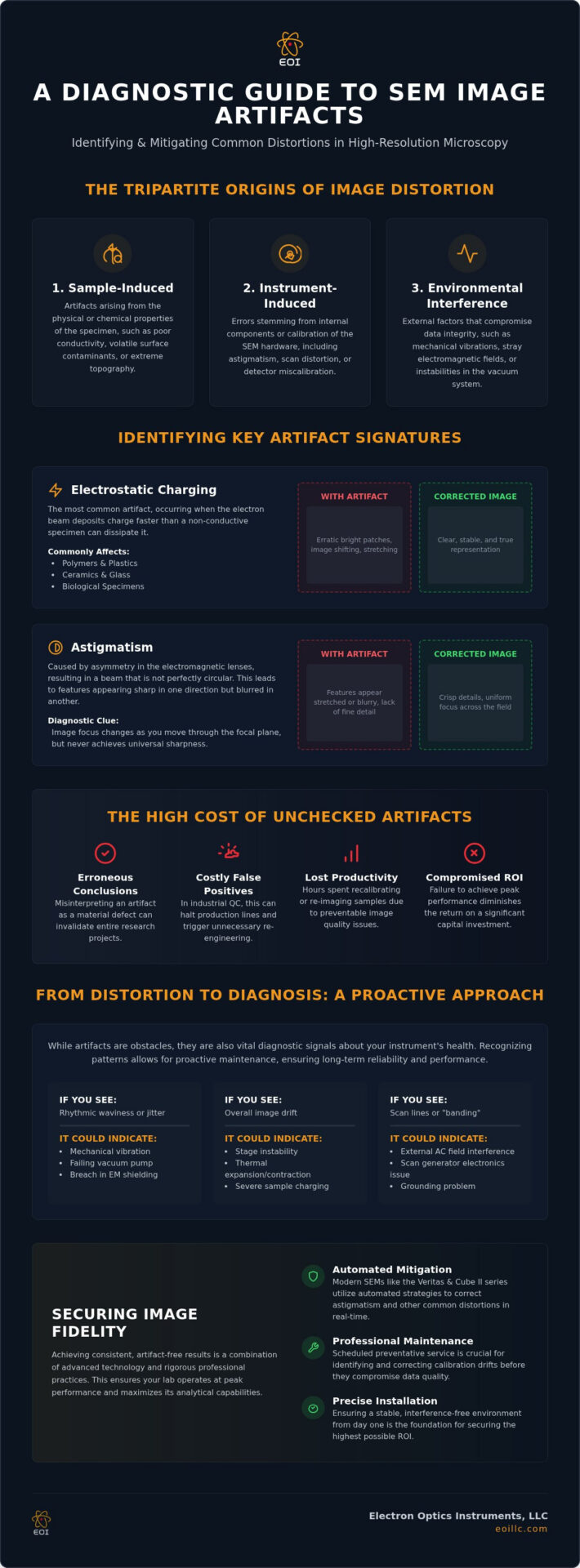
The taxonomy of these distortions generally falls into three distinct categories:
- Sample-induced: Distortions arising from the physical or chemical properties of the specimen, such as poor conductivity or volatile surface contaminants.
- Instrument-induced: Errors stemming from the internal components or calibration of the SEM scanning electron microscope hardware.
- Environmental interference: External factors like mechanical vibration or stray electromagnetic fields that penetrate the column shielding.
The Physics of Image Distortion
The visibility of Microscopy Artifacts is heavily influenced by the interaction volume and the specific signal detection method employed. Secondary electron (SE) imaging is particularly sensitive to surface-level charging and edge effects, whereas backscattered electron (BSE) signals may highlight compositional artifacts or shadowing. It’s helpful to differentiate between “false features,” which introduce non-existent data like ghosting or scan lines, and “information loss,” such as blurring that obscures critical details. In high-resolution microscopy, image fidelity is defined as the degree of exactness with which the electronic signal represents the physical specimen’s spatial and compositional properties without introducing synthetic aberrations.
Artifacts as Diagnostic Indicators
While distortions are often viewed as obstacles, they serve as vital diagnostic signals that reveal the health of the hardware. Specific errors often indicate that an instrument has drifted out of its optimal calibration state. For instance, a rhythmic waviness in the image might suggest a failing vacuum pump or a breach in electromagnetic shielding. The operator’s ability to recognize these patterns is essential for maintaining operational standards. Identifying these signals early allows labs to justify specialized service before minor drifts evolve into catastrophic instrument failure. This proactive approach, often enhanced by the visual clarity of Dextro Imaging Solutions diagnostic workstations, ensures that systems like the Veritas series or the Cube II continue to operate at their peak performance levels, securing the long-term reliability of the laboratory’s output.
Sample-Related Artifacts: Charging, Edge Effects, and Topography
Sample interaction remains the most frequent source of imaging anomalies in high-resolution microscopy. Among common sem image artifacts, electrostatic charging presents the most persistent challenge for laboratories analyzing non-conductive polymers, ceramics, or biological specimens. This phenomenon manifests as erratic bright patches, sudden image shifts, or “stretching” of the field of view, occurring when the primary electron beam deposits more charge than the specimen can effectively dissipate. Research from the National Institute of Standards and Technology emphasizes that SEM image distortions and artifacts often stem from these complex interactions between the electron probe and the specimen substrate, particularly when analyzing resist-heavy materials.
Beyond charging, the “edge effect” creates a deceptive visual profile where sharp protrusions or steep slopes appear unnaturally bright. This occurs because the geometry of the specimen allows for a higher escape probability of secondary electrons compared to flat surfaces. While this may highlight certain topographic features, it frequently obscures fine surface details through excessive contrast. Additionally, high-energy electron interactions can cause localized sample damage, appearing as “burn marks” or structural melting in beam-sensitive materials. Poorly prepared specimens may also suffer from outgassing, which degrades vacuum quality and results in the formation of “dark squares”-carbon contamination deposited on the region of interest during prolonged beam exposure.
Mitigating Charging without Sputter Coating
Operators can often resolve charging issues by strategically lowering the accelerating voltage (kV) to reach a “charge balance” point where the number of incident electrons equals the total emitted signal. The Veritas series offers sophisticated Variable Pressure (VP) modes, which introduce a controlled amount of gas into the chamber to neutralize surface charge through gaseous ionization. This capability is particularly advantageous for imaging porous or hydrated materials that cannot withstand traditional coating processes. Furthermore, adjusting the scan rate or dwell time prevents excessive charge accumulation in a single pixel area, preserving the integrity of the raw data.
The Importance of Proper Sample Preparation
Establishing robust conductive paths using silver paste or carbon tape is essential for facilitating electron dissipation and maintaining image stability. Mastering these mounting techniques requires specialized SEM operation training to ensure consistency across diverse specimen types. It’s a fundamental reality that maintaining absolute sample cleanliness is directly proportional to achieving long-term vacuum stability and preventing the deposition of hydrocarbon contaminants. For laboratories seeking to optimize their imaging fidelity, investing in high-performance SEM consumables can significantly reduce the occurrence of these avoidable distortions.
Instrument and Beam-Induced Artifacts: Mastering Resolution
While specimen preparation is a vital precursor to success, the internal electron optics of the system are equally responsible for image fidelity. Achieving sub-nanometer resolution requires an operator to distinguish between authentic specimen features and instrument-induced common sem image artifacts. These aberrations often arise from misaligned apertures or asymmetrical magnetic fields within the column. When an image appears to stretch or smear in a specific diagonal orientation while passing through the focal point, the system is likely suffering from astigmatism. This distortion is particularly prevalent when utilizing high-resolution platforms like the Veritas HR SEM, where even minute optical deviations are magnified at the extreme edge of the instrument’s capability.
Detector saturation represents another critical beam-induced issue that can compromise data integrity. When the gain on an Everhart-Thornley (ET) detector is set too high, the resulting image appears flat, with clipped highlights that obscure essential topographic detail. Similarly, aging electron sources impact the signal-to-noise ratio. A tungsten filament nearing the end of its 100 to 200-hour lifespan often exhibits emission instability, leading to ghosting or excessive graininess that masks the true nature of the specimen. Identifying these symptoms early prevents the misinterpretation of noise as actual material characteristics.
Correcting Astigmatism with the Stigmator
Correcting beam circularity is a non-negotiable prerequisite for any high-magnification analysis. To diagnose astigmatism, operators should observe the specimen while moving through the focal plane; if the image features elongate in one direction before focus and then rotate 90 degrees after focus, stigmator adjustment is required. It’s essential to recognize that carbon buildup on the final aperture can create localized electrostatic fields that mimic astigmatism. Maintaining a rigorous schedule for cleaning or replacing apertures is vital for ensuring the long-term optical precision of the Veritas series and preventing resolution loss.
Optimizing Beam Parameters
Successful industrial failure analysis depends on balancing the probe current, often referred to as spot size, with the required resolution. A larger spot size increases signal strength but sacrifices the fine detail necessary for nanometric characterization. Modern platforms like the Cube II benchtop SEM integrate automated alignment sequences that significantly reduce these operator-induced aberrations, allowing for faster diagnostic workflows and more consistent results. Distinguishing between electronic noise and actual signal in low-light imaging conditions remains a hallmark of a skilled microscopist. By refining these parameters, laboratories ensure their instrumentation delivers the high-fidelity data required for international production standards.
Environmental Artifacts: Vibration, Stray Fields, and Vacuum Leaks
Environmental stability serves as the fundamental bedrock of high-fidelity imaging, yet external variables remain a frequent source of diagnostic confusion in industrial laboratories. Disturbances originating outside the microscope column often manifest as common sem image artifacts that an inexperienced operator might mistakenly attribute to specimen preparation errors. Mechanical vibration, for instance, typically presents as a “sawtooth” jaggedness on vertical edges or a periodic blurring of the entire scan area. These disturbances are frequently traced back to building infrastructure, such as reciprocating HVAC compressors, mechanical vacuum pumps, or even rhythmic foot traffic in high-density corridors.
Electromagnetic Interference (EMI) introduces a distinct rhythmic “waviness” or moiré pattern into the micrograph, often synchronized with the 50/60 Hz frequency of nearby unshielded power lines or heavy industrial equipment. While often overlooked, acoustic noise from high-decibel environments can also induce micro-vibrations within the column of a high-resolution system, leading to a subtle but measurable loss of resolution at extreme magnifications. Identifying these environmental signatures is essential for maintaining the rigorous standards required for failure analysis and materials characterization.
Isolating the Microscope Environment
Securing a stable analytical environment requires a strategic approach to laboratory site selection and hardware integration. The implementation of passive or active vibration isolation tables is a standard prerequisite for research-grade systems like the Veritas series. Interestingly, the compact architecture of a modern desktop SEM offers a significant structural advantage in this regard, as its integrated dampening systems and lower center of gravity make it inherently less susceptible to low-frequency floor noise. Identifying EMI signatures during the initial installation phase prevents long-term operational frustration and ensures the integrity of the collected data.
Diagnosing Vacuum-Related Image Noise
Vacuum integrity is critical for maintaining a clear mean free path for the primary electron beam. When vacuum levels are compromised by slow leaks or aging seals, increased electron scattering occurs, resulting in a “foggy” or low-contrast image that lacks sharp definition. Oil backstreaming from traditional rotary pumps can also introduce hydrocarbon contaminants that permanently degrade sensitive detector surfaces. Utilizing dry scroll pumps is the most effective strategy for maintaining artifact-free imaging environments because they eliminate the risk of oil-related contamination while providing a more stable vacuum baseline. If your laboratory is experiencing persistent imaging anomalies, our team provides comprehensive SEM preventative maintenance and site surveys to isolate and resolve environmental interference.
Mitigating Artifacts through Advanced Hardware and Professional Service
Resolution of imaging anomalies shouldn’t be viewed merely as a troubleshooting exercise but as a strategic commitment to instrument health. While previous sections detailed the specific signatures of common sem image artifacts, the most effective mitigation strategy involves the intersection of advanced hardware architecture and rigorous professional oversight. Modern platforms, specifically the Cube II and Genesis series, are engineered to internalize many of the corrective measures that once required intensive manual intervention. By automating the alignment of electron optics and optimizing vacuum cycles, these systems provide a stable baseline that minimizes the impact of operator variability and environmental flux.
Beyond the hardware, the longevity of analytical fidelity depends on the meticulousness of professional service. Professional installation and relocation services are vital because they ensure that the instrument’s shielding and isolation systems are perfectly tuned to the specific electromagnetic and mechanical profile of the laboratory. Annual service contracts act as a preemptive strike against the gradual accumulation of column contamination and the inevitable degradation of electron sources. This systematic approach to the reduction of common sem image artifacts transforms distortions from recurring obstacles into manageable diagnostic indicators that signal when a system requires preventative care.
The Cube II Advantage: Integrated Stability
The Cube II benchtop SEM distinguishes itself through an architectural synergy of low-vibration turbomolecular pumps and a vacuum system designed for rapid throughput without compromising stability. Its optimized column geometry provides inherent resistance to the mechanical noise that often plagues larger, less integrated systems. The intuitive software interface acts as a digital guide, leading users through complex alignment and focus routines that traditionally required years of specialized expertise. For high-throughput industrial laboratories, this integration ensures that high-resolution data remains consistent across multiple shifts and various operator skill levels.
Ensuring Long-Term Imaging Excellence
Investing in proactive care is the most effective way to manage the total electron microscope cost in 2026. Frequent preventative maintenance visits by Electron Optics Instruments technicians ensure that aperture clusters remain clean and vacuum seals stay airtight, directly extending the operational life of the unit. On-site technical training further bridges the gap between basic operation and expert microscopy, empowering your team to identify and resolve user-induced distortions before they compromise research outcomes. To secure the highest fidelity for your laboratory’s future, Contact Electron Optics Instruments for a technical consultation or SEM quote.
Advancing Analytical Fidelity through Diagnostic Precision
Achieving nanometric clarity requires more than high-performance hardware; it demands a systematic understanding of how common sem image artifacts compromise data integrity. By distinguishing between sample-induced charging and environmental interference, you secure the reliability of your failure analysis and research outcomes. This transition from basic imaging to expert microscopy is the foundation of institutional progress and technical authority. It’s a process that balances the meticulousness of the operator with the inherent stability of the instrument.
With over 30 years of technical expertise, Electron Optics Instruments, LLC serves as the sole US distributor for EmCraft, offering specialized on-site training and preventative maintenance contracts that ensure long-term stability. Our commitment to meticulousness means your laboratory can focus on innovation while we handle the complexities of instrumental calibration. Request a Quote for the Cube II Benchtop SEM to integrate these advanced diagnostic capabilities into your facility today. Your path to absolute imaging fidelity starts with a partner dedicated to international production excellence and visionary hardware solutions.
Frequently Asked Questions
What is the most common cause of image artifacts in benchtop SEMs?
Sample charging is the most frequent cause of artifacts in benchtop systems like the Cube II. While these instruments feature advanced integrated shielding, the inherent non-conductive nature of many industrial specimens leads to electrostatic accumulation. This results in bright patches or image instability. Addressing this requires careful management of accelerating voltage or the use of variable pressure modes to neutralize surface charge before it compromises the resolution.
How can I tell the difference between sample charging and a mechanical vibration issue?
You can distinguish between these by observing the visual pattern of the distortion. Charging typically manifests as erratic, bright flashes or sudden shifts in the field of view that occur randomly. In contrast, mechanical vibration presents as a rhythmic, sawtooth jaggedness on vertical edges or a consistent periodic blurring. Vibration artifacts are often synchronized with external sources like pumps or HVAC systems, whereas charging is an interaction between the beam and the specimen.
Does astigmatism always mean my SEM column is dirty?
Astigmatism doesn’t always indicate a contaminated column, although a dirty final aperture is a frequent culprit. This aberration often results from asymmetrical magnetic fields within the lenses or minor misalignments in the optical path. While routine maintenance is essential to prevent carbon buildup, operators can usually correct minor astigmatism using the stigmator controls. If the distortion persists after adjustment, it may signal that a professional preventative maintenance visit is necessary to clean the internal components.
Why do my SEM images look “grainy” even at low magnification?
Graininess at low magnification is usually a symptom of a low signal-to-noise ratio rather than a resolution limit. This often occurs when the probe current is set too low or the scan speed is too fast for the detector to collect sufficient electrons. To resolve this, you should increase the dwell time or adjust the spot size to enhance signal collection. Persistent noise may also indicate that the electron source, such as a tungsten filament, is nearing the end of its operational lifespan.
Can improper sample preparation cause vacuum-related artifacts?
Improper sample preparation is a primary driver of vacuum-related common sem image artifacts. Specimens that aren’t thoroughly dried or cleaned can outgas volatile compounds once the chamber reaches high vacuum levels. This outgassing increases electron scattering, which produces a foggy image with reduced contrast. Additionally, hydrocarbons from the sample can deposit on the region of interest under the electron beam, creating dark contamination squares that permanently obscure fine surface details.
How does accelerating voltage (kV) affect the visibility of artifacts?
Adjusting the accelerating voltage directly dictates the interaction volume and the severity of certain common sem image artifacts. Higher kV settings increase beam penetration, which can exacerbate charging on non-conductive materials and potentially cause beam damage or melting in sensitive specimens. Conversely, lowering the kV reduces these effects but may limit the resolution of the image. Finding the charge balance point where emission equals deposition is critical for achieving high-fidelity results without resorting to destructive coating methods.
What are “ghost images” in SEM and how are they prevented?
Ghost images in SEM are secondary, faint outlines of features that appear offset from the primary subject. These are typically caused by stray electronic signals or reflections within the detector electronics, but they can also result from extreme charging where the accumulated field deflects the primary beam. Preventing these requires ensuring proper grounding of the specimen and maintaining the health of the ET detector. High-end systems like the Veritas series utilize advanced signal processing to minimize these electronic echoes.
Is it possible to remove artifacts from an SEM image using post-processing software?
While post-processing software can reduce noise or improve contrast, it cannot authentically remove structural artifacts like astigmatism or mechanical vibration. Digital filters often introduce their own distortions, potentially leading to the misinterpretation of data during industrial failure analysis. The most reliable approach is to mitigate artifacts at the source through proper instrument calibration and specimen preparation. Software should be used as a tool for enhancement rather than a substitute for capturing a high-fidelity raw image.