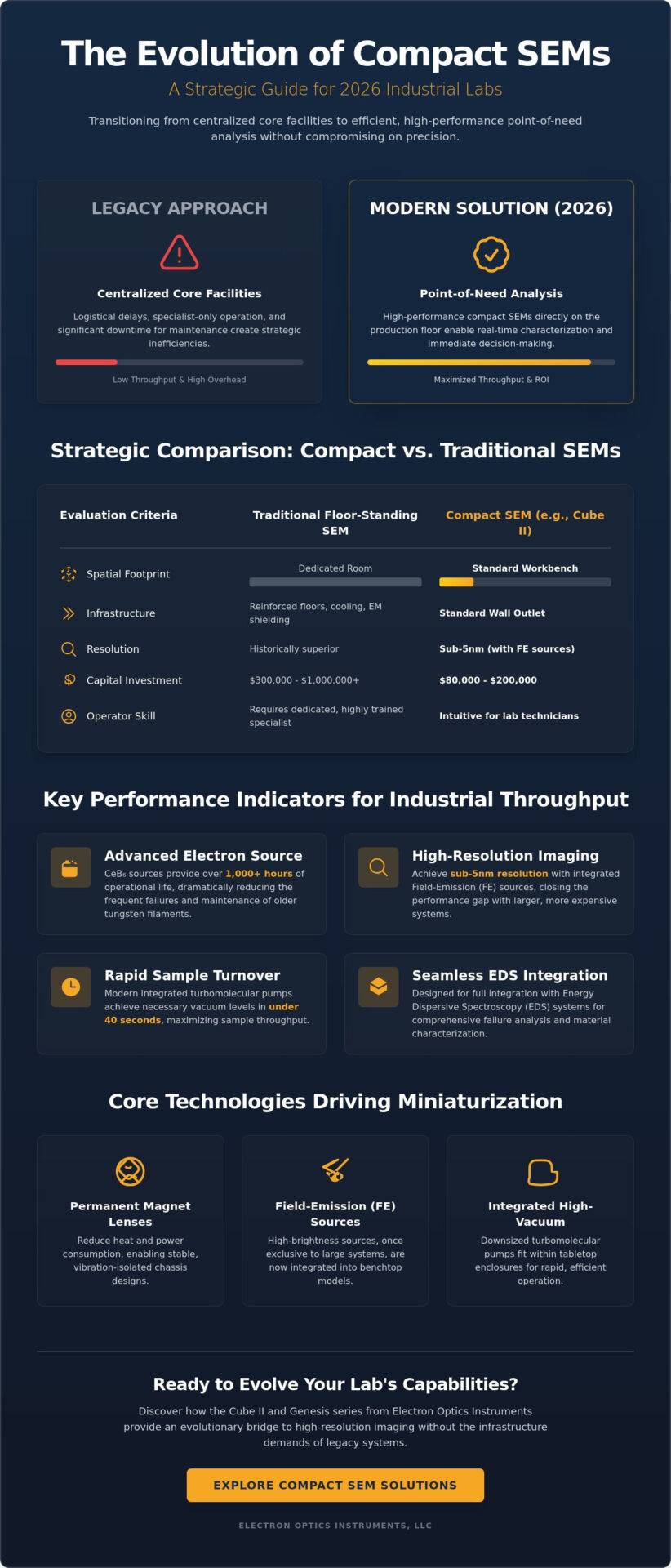
By the midpoint of 2026, the necessity for expansive, floor-standing microscopy suites has transitioned from an industry standard to a strategic inefficiency. You’ve likely encountered the persistent challenge of integrating high-resolution imaging into modern facilities where space is at a premium and downtime for legacy system maintenance is unacceptable. Investing in a compact sem for industrial labs represents an evolutionary leap that bridges the gap between traditional spatial constraints and the demand for sub-10nm analytical precision.
This strategic guide outlines the critical variables required to maximize your laboratory’s throughput, ensuring your next acquisition offers the sub-5nm resolution and seamless EDS integration found in the Veritas FE and Cube II series. We’ll examine how current 2026 benchmarks, including the February 15 update to ASTM E 3 and the emerging ISO/DIS 16887:2026 standards, influence the total cost of ownership. You’ll gain the insight needed to identify a system that balances the $80,000 to $200,000 capital investment with the long-term reliability of advanced electron sources like CeB6, which now provide over 1,000 hours of operational life without the frequent failures associated with older tungsten filaments.
Key Takeaways
- Identify the strategic transition from centralized core facilities to point-of-need testing that utilizes high-performance instrumentation with a significantly reduced spatial footprint.
- Determine the specific resolution and magnification parameters required to optimize failure analysis while ensuring seamless integration with Energy Dispersive Spectroscopy (EDS) systems.
- Evaluate the technical distinctions between desktop and tabletop models to select the most efficient compact sem for industrial labs based on your specific throughput and screening objectives.
- Master the essential site preparation and preventative maintenance protocols necessary to ensure long-term operational reliability and maximize the return on your analytical investment.
- Explore how advanced platforms like the Cube II and Genesis series provide an evolutionary bridge to high-resolution imaging without the infrastructure demands of legacy systems.
The Evolution of Compact Scanning Electron Microscopy in Industrial Environments
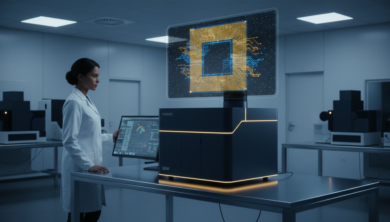
The industrial landscape of 2026 has witnessed a fundamental shift in analytical workflows, moving away from the logistical delays inherent in centralized core facilities toward a point-of-need model. A compact sem for industrial labs is no longer a compromised alternative to larger systems; it’s a high-performance instrument that delivers precision imaging within a fraction of the traditional floor-model footprint. This evolution enables manufacturing facilities to conduct real-time characterization directly on the production floor, facilitating immediate decision-making in sectors where microscopic defects lead to catastrophic failures.
Advancements in electron optics have effectively narrowed the historical performance gap that once separated benchtop units from their expansive counterparts. By utilizing a Scanning Electron Microscope (SEM) with modern miniaturized components, engineers achieve the same analytical rigor previously reserved for specialized research institutions. This paradigm shift is driven by a requirement for sustainable innovation and global manufacturing excellence, where speed and precision act as the primary metrics of corporate success.
The Drivers of Miniaturization
The transition to compact architectures stems from several engineering breakthroughs that have reached maturity by May 2026. Key technological drivers include:
- Permanent Magnet Lenses: These components reduce the heat generation and power consumption typical of traditional electromagnetic coils, allowing for a more stable, vibration-isolated chassis.
- Field-Emission (FE) Sources: High-brightness FE sources, once exclusive to large-scale systems, are now integrated into benchtop models like the Veritas FE, providing resolution down to 5nm.
- Integrated High-Vacuum Systems: Modern turbomolecular pumps have been downsized to fit within tabletop enclosures, achieving necessary vacuum levels in under 40 seconds to maximize sample turnover.
Industrial demand in the semiconductor and solid-state battery sectors has accelerated this trend. These fields require rapid, high-resolution feedback to maintain yield rates in the competitive 2026 market, making the integration of compact systems a strategic necessity rather than a luxury.
Compact SEM vs. Traditional Floor Models
Traditional floor-standing microscopes often demand dedicated rooms with reinforced flooring, specialized cooling systems, and rigorous electromagnetic shielding. In contrast, modern compact units operate on standard wall outlets and fit onto existing laboratory workbenches without extensive facility modifications. The shift isn’t merely physical. It represents a transition from specialist-only operation to intuitive, automated interfaces that allow lab technicians to produce reliable data without years of specialized training. The evolution of the compact SEM directly catalyzes industrial throughput by decentralizing high-resolution analysis and embedding it within the active manufacturing lifecycle. As of January 2026, these systems provide a superior return on investment by eliminating the logistical bottlenecks of off-site testing while maintaining the rigorous standards required by the February 2026 update to ASTM E 3.
Key Performance Indicators: Evaluating Compact SEMs for Industrial Throughput
In the high-stakes environment of 2026 industrial manufacturing, the efficacy of a compact sem for industrial labs is measured by its ability to convert raw samples into actionable data with minimal latency. Analytical precision is no longer a secondary concern; it’s the primary driver of quality control and failure analysis. To achieve optimal throughput, decision-makers must evaluate instrumentation based on specific performance indicators that align with their operational requirements, focusing on source longevity and automated integration.
Reliability in vacuum architectures remains a cornerstone of industrial utility. Modern systems achieve a time-to-image of under 40 seconds, a metric that encompasses sample loading and vacuum cycling. This speed is essential for high-volume screening where manual intervention must be minimized. Software automation has evolved to include AI-assisted focusing and automated stage movements, effectively reducing the “human-in-the-loop” bottleneck that historically limited SEM productivity.
Resolution and Source Technology
The choice of electron source dictates the instrument’s resolution limits and long-term operating costs. While tungsten filaments remain a low-cost entry point at approximately $50 to $100 per unit, their limited 100 to 200-hour lifespan often creates unacceptable maintenance intervals for 24/7 industrial operations. In contrast, CeB6 sources, although requiring a higher initial investment between $1,000 and $2,000, provide over 1,000 hours of stable operation. Recent advances in tabletop SEM technology have also integrated Field Emission (FEG) sources into compact frames, enabling sub-5nm resolution at lower acceleration voltages.
Determining the appropriate kV range is critical for material-specific analysis. Polymers and biological samples often require low-voltage imaging (0.5kV to 5kV) to prevent beam damage, whereas metallurgical applications typically necessitate higher voltages (15kV to 30kV) for deeper penetration and effective signal generation. High-sensitivity detectors now allow for rapid acquisition even at these lower dosages, ensuring that image quality doesn’t degrade during high-speed screening. Selecting the right compact sem for industrial labs ensures these technical parameters are met without the spatial requirements of legacy equipment.
Integrated Analytical Capabilities
Material characterization in 2026 demands more than just topographical imaging. The integration of Energy Dispersive Spectroscopy (EDS) is now a standard requirement for identifying elemental composition during failure analysis. A seamless EDS interface allows for real-time mapping, enabling technicians to correlate morphological defects with chemical impurities instantly. This synergy is further enhanced by Backscattered Electron (BSE) detectors, which provide immediate visual contrast based on atomic number differences.
For facilities managing complex alloys or semiconductor components, mastering advanced SEM techniques is essential for maintaining a competitive edge. These methodologies ensure that compositional data is both quantitative and reproducible, adhering to ISO 16700:2016 calibration standards. If your facility requires this level of precision, exploring high-performance electron optics solutions provides a clear path toward analytical excellence without the infrastructure burden of traditional floor models.
Desktop vs. Tabletop vs. Floor-Standing: A Strategic Comparison
Selecting the appropriate form factor for a compact sem for industrial labs requires a nuanced understanding of how physical architecture influences analytical capability. While the distinction between desktop, tabletop, and floor-standing models was once defined by a stark performance gap, 2026 technology has effectively blurred these lines, offering high-resolution imaging across all tiers. The decision-making process now hinges on the specific synergy between sample dimensions, throughput requirements, and the necessary degree of modularity for future technical upgrades.
Desktop models represent the pinnacle of space-saving engineering, designed specifically for rapid screening where time-to-image is the critical metric. These units typically feature simplified vacuum systems and automated interfaces that facilitate high-volume throughput for non-specialist operators. Tabletop or benchtop systems, such as the Cube II, serve as the primary industrial workhorse, providing a broader range of acceleration voltages and enhanced detector integration. For facilities requiring maximum chamber volume to accommodate large engineering components or multi-sample holders, compact floor-standing models like the Veritas series offer the modularity of traditional systems within a footprint that remains compatible with standard laboratory environments.
Selecting the Right Tier for Your Lab
Strategic procurement must account for the total cost of electron microscope ownership, which encompasses initial capital expenditure, consumable filaments, and long-term maintenance. High-volume industrial environments often favor systems with larger chambers to reduce the frequency of venting and pumping cycles. Future-proofing an investment involves selecting a platform that supports modular additions, such as EBSD or specialized cooling stages, ensuring the instrument evolves alongside the facility’s analytical requirements. Concurrently, labs must verify that their chosen system adheres to the updated ASTM E 3 standards published on February 15, 2026, to guarantee regulatory compliance in metallographic preparation.
Industrial Use Case Examples
The diversity of Scanning Electron Microscopy Applications dictates the ideal form factor for specific sectors. In semiconductor failure analysis, where sub-5nm resolution is mandatory, a field-emission (FE) tabletop system provides the necessary precision without the infrastructure costs of a full-scale suite. Additive manufacturing labs, however, often prioritize compact floor-standing models to accommodate bulky 3D-printed metal parts that exceed the chamber limits of desktop units. Pharmaceutical facilities frequently leverage the automation of desktop SEMs for particle sizing and shape analysis, where the priority is standardized, repeatable data collection across multiple production shifts. This tiered approach ensures that every compact sem for industrial labs is precisely calibrated to the operational realities of its specific manufacturing environment.
Operational Implementation: Site Preparation, Maintenance, and TCO
Successful deployment of a compact sem for industrial labs extends beyond the initial capital expenditure. It requires a structured approach to facility integration and long-term asset management. While these instruments are engineered for standard laboratory environments, achieving the sub-10nm resolution promised by the Veritas FE series requires meticulous attention to the electromagnetic and vibrational profile of the installation site. Industrial zones often present challenges such as heavy machinery interference or fluctuating power grids that can degrade image quality if not addressed during the site preparation phase.
Operational excellence in 2026 is defined by the synergy between advanced hardware and professional SEM operation. Although modern interfaces have lowered the barrier to entry, maintaining the rigorous data integrity required by ISO/TS 21383 for quantitative measurements necessitates formal technician training. This professionalization ensures that the high throughput capabilities of the Cube II or Genesis systems aren’t undermined by improper sample preparation or suboptimal beam settings. Calculating the total cost of ownership (TCO) must therefore include these human capital investments alongside the hard costs of consumables and service contracts.
Installation and Relocation Logistics
The transition from delivery to first-image involves critical calibration steps to meet established ISO 16700:2016 magnification standards. Professional handling is mandatory during decommissioning and transport; even minor shocks can misalign the sensitive electron optics within a compact chassis. Post-installation, labs must conduct a comprehensive re-validation to ensure the system performs to its 2026 specifications within its new environment. Managing electromagnetic interference (EMI) is particularly vital in automotive or aerospace manufacturing facilities where high-current equipment is frequently in operation nearby.
Maintenance and Service Contracts
Uptime is the most significant variable in the TCO equation for industrial facilities. Implementing a schedule for preventative SEM maintenance mitigates the risk of catastrophic vacuum failure or source depletion during critical production runs. In the current 2026 market, maintenance strategies have evolved to include:
- Remote Diagnostic Capabilities: Many systems now allow for real-time monitoring of vacuum levels and filament health, enabling preemptive service before a failure occurs.
- Tiered Service Agreements: These contracts balance the need for priority on-site repairs with the budgetary realities of smaller industrial labs.
- Consumable Management: Factoring in the $1,000 to $2,000 cost of CeB6 sources against their 1,000-hour lifespan is essential for accurate annual budgeting compared to the more frequent changes required by $50 tungsten filaments.
Ensuring the longevity of your analytical precision requires a partner who understands the grounded, practical realities of global manufacturing. To secure your facility’s analytical future, schedule a consultation for a customized SEM maintenance and support plan.
The Electron Optics Instruments Solution: Cube II and Beyond
Selecting the optimal compact sem for industrial labs requires a partner that possesses both technical depth and a comprehensive understanding of global manufacturing workflows. With a legacy spanning 30 years, Electron Optics Instruments, LLC has established itself as a visionary authority in the field of electron optics, providing the precision required for modern automotive and semiconductor sectors. Our portfolio is engineered to meet the evolutionary demands of 2026 industrial environments, where the synergy between high-resolution imaging and operational reliability is paramount for maintaining a competitive edge.
The Cube II Benchtop SEM serves as the cornerstone of our compact offerings, delivering high-performance imaging within an exceptionally small chassis. It features a 5-axis stage and achieves a 5nm resolution, making it the premier choice for facilities that require research-grade data without the infrastructure of a traditional microscopy suite. For organizations focused on high-volume routine screening, the Genesis Tabletop SEM acts as the industrial workhorse. It’s designed for rapid characterization and ease of use, ensuring that lab technicians can maintain high throughput without compromising the accuracy of their material analysis.
For laboratories engaged in advanced material research, the Veritas Series represents the pinnacle of compact electron optics. This series, which includes the Veritas FE and Veritas HR, provides an evolutionary leap in resolution and analytical capability. These systems are specifically configured to handle the rigorous demands of failure analysis and quality control, ensuring that every microscopic detail is captured with absolute clarity. By integrating these advanced platforms, industrial labs can achieve a level of precision that was previously the exclusive domain of large-scale research institutions.
Unmatched Service and Technical Support
Our commitment to excellence extends far beyond the initial equipment acquisition. Electron Optics Instruments, LLC provides comprehensive service contracts that encompass all major SEM brands, ensuring that your entire analytical suite remains operational with minimal downtime. Our technical experts deliver on-site training tailored to your specific industrial applications, maximizing your team’s productivity from the first day of installation. We specialize in customized EDS integration, allowing for seamless elemental mapping and material characterization that adheres to the most stringent 2026 ISO and ASTM standards.
Ready to Evolve Your Industrial Lab?
The transition to a high-performance compact sem for industrial labs is a strategic investment in your facility’s future analytical capacity. Electron Optics Instruments, LLC is the sole US distributor for EmCraft SEMs, offering a unique bridge to innovative South Korean engineering backed by local support. Our applications scientists are available to provide technical consultations and live demonstrations, ensuring your selected system aligns perfectly with your throughput and resolution requirements. Whether you’re exploring our latest Veritas series or considering our inventory of meticulously refurbished SEM units, we provide the expertise needed to optimize your laboratory’s performance. Consult with Electron Optics Instruments, LLC for your compact SEM needs today to begin your laboratory’s evolutionary journey toward analytical precision.
Securing Analytical Precision in the 2026 Industrial Landscape
The paradigm shift toward decentralized microscopy is no longer just a trend; it’s a fundamental requirement for 2026 industrial resilience. Integrating a compact sem for industrial labs allows facilities to maintain the sub-10nm precision necessary for modern failure analysis without the logistical delays of off-site testing. By aligning your laboratory with the latest February 2026 standards, you ensure that your quality control data remains both quantitative and legally defensible in an increasingly competitive global market. In such a competitive environment, many organizations also leverage professional tradeshow booth kits to showcase their advanced analytical capabilities and technological leadership at international exhibitions.
For businesses navigating this global landscape, maintaining quality extends beyond the lab to the production source; partnering with The Inspection Company can help ensure that international manufacturing partners consistently meet your rigorous technical specifications through professional factory audits.
Electron Optics Instruments, LLC offers the technical authority and 30 years of experience needed to guide your team through this technological evolution. As the sole US distributor for EmCraft SEMs and a provider of comprehensive service for all major manufacturers, we provide a unified support structure for your entire analytical suite. It’s time to leverage these advancements to enhance your throughput and secure your facility’s position as a leader in technical innovation. Explore the Cube II and Genesis Series at Electron Optics Instruments, LLC to begin your laboratory’s evolutionary journey toward unmatched precision.
Frequently Asked Questions
What is the typical resolution of a compact SEM in 2026?
High-performance compact systems in 2026 reach resolutions as fine as 5nm when equipped with field-emission sources. This capability allows industrial labs to analyze nanostructures that previously required massive floor-standing units. Standard tungsten-based tabletop models typically provide resolution in the 10nm to 15nm range, which remains sufficient for the majority of routine metallurgical and polymer inspections where extreme magnification isn’t the primary requirement.
Can a compact SEM perform full Energy Dispersive Spectroscopy (EDS) analysis?
Modern compact units perform full Energy Dispersive Spectroscopy (EDS) for both qualitative and quantitative elemental mapping. The integration of high-sensitivity silicon drift detectors (SDD) allows for rapid data collection and real-time compositional overlays. This seamless analytical capability is essential for identifying microscopic contaminants or verifying alloy concentrations during the failure analysis process in 2026 manufacturing environments where material integrity is paramount.
How does the maintenance of a compact SEM differ from a floor model?
Maintenance for a compact sem for industrial labs is streamlined due to the use of dry vacuum pumps and miniaturized column designs. Unlike traditional floor models that require complex water-cooling systems and frequent oil changes, compact units focus on filament replacement and occasional aperture cleaning. However, professional preventative maintenance visits are still required annually to validate magnification calibration and ensure adherence to ISO 16700:2016 standards.
What are the power and facility requirements for a tabletop SEM?
Most tabletop SEMs operate on a single, standard 100V to 240V AC power outlet and don’t require specialized facility modifications. These systems are designed for sustainable innovation, consuming significantly less power than legacy instruments while eliminating the need for external compressed air or water lines. While they include internal vibration isolation, placing the unit on a vibration-damped table is recommended for achieving maximum resolution in high-traffic industrial zones.
Is a compact SEM suitable for high-throughput industrial quality control?
A compact sem for industrial labs is highly suitable for high-throughput quality control due to its rapid vacuum cycling and automated imaging software. Features like automated multi-sample stage movements allow non-specialist operators to collect high-resolution data across dozens of samples per shift. This efficiency is critical for maintaining yield rates in semiconductor and battery manufacturing where real-time microscopic feedback is a strategic necessity for global manufacturing excellence.
How long does a typical compact SEM installation take?
The installation of a compact system typically takes 1 to 2 business days from delivery to operational status. This period includes the physical assembly of the unit, vacuum system stabilization, and rigorous calibration to meet the February 15, 2026, update to ASTM E 3 standards. Our application scientists also conduct comprehensive on-site training during this window to ensure your lab personnel are proficient in both imaging and basic system diagnostics.
Can I upgrade my compact SEM with additional detectors later?
Modular architectures in 2026 allow for the subsequent addition of various detectors and stages as your analytical needs evolve. You can upgrade a base system with backscattered electron (BSE) detectors, low-vacuum modes, or specialized cooling stages for non-conductive samples. This flexibility ensures that your initial investment remains relevant as your facility expands its material characterization capabilities or adopts new global manufacturing standards over the next decade.
What is the average lifespan of an industrial compact SEM source?
Electron source lifespan is dictated by the cathode technology, with tungsten filaments providing approximately 100 to 200 hours of operation. CeB6 sources, found in many high-performance tabletop models, offer a significantly longer lifetime exceeding 1,000 hours of stable beam current. For the highest reliability, field-emission guns used in the Veritas FE series can operate for over 5,000 hours before requiring professional service, effectively minimizing instrument downtime in 24/7 industrial settings.