
Approximately 65% of sub-optimal imaging outcomes in industrial laboratories are attributed directly to failures in sample preparation rather than inherent hardware limitations. Achieving consistent high resolution sem performance remains a significant challenge for researchers who must balance the meticulous demands of electron optics with the practical realities of laboratory throughput. You’re likely aware that maintaining sub-5nm precision is not merely a matter of hardware acquisition; it’s a systemic discipline that requires a deep integration of technical expertise and environmental control. The struggle to maintain peak resolution while managing the substantial capital requirements of traditional floor-model systems often complicates these strategic objectives.
This professional guide provides the technical framework necessary to master these nuances, ensuring your facility maximizes its analytical precision and capitalizes on the return on investment of advanced instrumentation. We’ll examine the critical synergy between sample preparation protocols and electron optics, explore the specific capabilities of systems like the Veritas and Cube II series, and outline the maintenance strategies required to sustain peak imaging standards throughout 2026. By aligning your operational protocols with the latest advancements in benchtop and floor-model technology, you’ll achieve the reliable, high-end results your research demands.
Key Takeaways
- Establish a sophisticated understanding of the 2026 technical standards that differentiate theoretical instrument specifications from the practical image clarity required in complex industrial environments.
- Analyze how the intricate convergence of electron beam probe size, interaction volume, and vacuum integrity dictates the ultimate limits of nanoscale imaging precision and analytical accuracy.
- Develop a strategic framework for selecting between the ultra-high performance of the Veritas series and the innovative, high-resolution capabilities of the Cube II benchtop system based on specific laboratory requirements.
- Ensure the long-term operational integrity of your laboratory’s high resolution sem by implementing rigorous preventative maintenance schedules that prioritize vacuum integrity and filament stability.
- Optimize research throughput by integrating advanced sample preparation techniques that mitigate the 65% of imaging failures typically caused by preparation inconsistencies within specialized industrial sectors.
Defining High-Resolution SEM: Beyond the Nanometer Scale in 2026
In the current industrial landscape of 2026, high resolution sem is defined less by a single metric and more by the systemic integration of electron optics, vacuum stability, and signal processing. While historical definitions often focused solely on the theoretical limit of the electron probe, modern standards require the consistent attainment of sub-5nm resolution in practical, real-world applications. A Scanning Electron Microscope (SEM) achieves this through a complex interplay of hardware precision and environmental control. It’s vital to distinguish between instrument resolution, which represents the hardware’s ultimate potential under ideal conditions, and image resolution, which is the actual clarity achieved on the digital output. The latter is heavily influenced by contrast and signal-to-noise ratios; without sufficient contrast, even the most precisely focused beam cannot distinguish individual nanoscale features from the surrounding sample matrix.
The Evolution of High-Resolution Standards
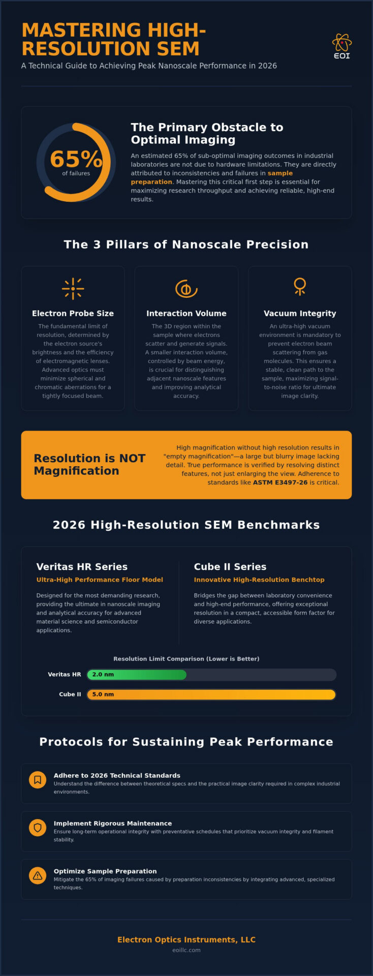
The trajectory of microscopy has shifted decisively from micro-scale observations to the rigorous demands of sub-nanometer imaging. Within the semiconductor and biotechnology sectors, 2026 research protocols require more than simple morphology; they demand “analytical resolution.” This concept encompasses the ability to not only visualize a feature but to accurately map its elemental composition through integrated EDS systems. Current industry benchmarks place high-end floor models, such as the Veritas HR, at a 2.0 nm resolution limit, while leading benchtop systems like the Cube II have achieved a 5.0 nm standard. This progress effectively bridges the gap between laboratory convenience and the high-end performance required for advanced material science.
Resolution vs. Magnification: Correcting Common Misconceptions
A frequent error in equipment procurement involves conflating high magnification with high resolution. High magnification simply increases the size of the projected image area, but without a sufficiently small probe size and stable vacuum integrity, this results in “empty magnification.” In these instances, the image appears larger but lacks any additional structural detail, often appearing blurred or pixelated. To verify manufacturer claims during the selection process, professionals should look for adherence to updated standards such as ASTM E3497-26. Verification typically involves imaging gold-on-carbon standards to demonstrate that the system can resolve distinct particles at the stated limits. Relying on magnification figures alone is insufficient for high-stakes industrial research where meticulous accuracy is the primary objective.
The Determinants of Resolution: Probe Size, Interaction Volume, and Vacuum Integrity
The fundamental limit of any high resolution sem is governed by the diameter of the electron probe as it strikes the specimen surface. This probe size is determined by the electron source’s brightness and the efficiency of the electromagnetic lenses in demagnifying the source image. Modern optics must aggressively minimize spherical and chromatic aberrations; spherical aberrations occur when electrons at the beam’s periphery focus at different points than those in the center, while chromatic aberrations result from slight variations in electron energy. By utilizing advanced aperture designs and optimized column geometries, systems like the Veritas series achieve the tight, coherent beams necessary for sub-nanometer interrogation.
Resolution isn’t solely a function of the beam’s diameter. It’s also constrained by the interaction volume, the three-dimensional region within the sample where electrons scatter and generate signals. As the primary beam penetrates the sample, it spreads laterally; if this volume is too large, the resulting signal originates from an area wider than the probe itself, blurring fine details. Achieving superior clarity requires low-voltage imaging techniques that confine the interaction volume to the immediate surface of the specimen. Maintaining this precision requires absolute vacuum integrity. Any residual gas molecules in the column can deflect electrons, causing beam skirt and reducing the intensity of the primary probe.
Electron Source Technology: Tungsten vs. Field Emission (FEG)
While tungsten filaments offer reliability for general applications, Field Emission (FE) sources are the definitive standard for nanoscale imaging. FEGs provide a source brightness orders of magnitude higher than thermionic emitters, allowing for a much smaller spot size even at low accelerating voltages. The Veritas FE SEM utilizes these advanced sources to provide the stability and longevity required for prolonged research sessions. This technology ensures that the beam remains monochromatic and tightly focused, which is essential for resolving features that fall below the 5nm threshold.
The Role of Secondary and Backscattered Electron Detection
Detector sensitivity dictates the effective resolution of the final image. High-resolution environments often employ in-lens detectors that capture secondary electrons (SE) directly within the objective lens, minimizing signal loss and maximizing topographic contrast. Optimizing the signal-to-noise ratio (SNR) is essential; a weak signal leads to grainy images that obscure the very features the system is designed to resolve. Laboratories looking to sustain these rigorous imaging standards often invest in preventative maintenance visits to ensure their optical alignment and detector efficiency remain at peak performance levels.
Evaluating High-Resolution Benchtop vs. Floor-Model SEM Performance
Selecting the optimal high resolution sem architecture necessitates a strategic assessment of both analytical requirements and facility infrastructure. For many industrial laboratories, the choice between a compact benchtop unit and a sophisticated floor-model system hinges on the balance between spatial versatility and the absolute limits of nanoscale resolution. While traditional floor models were once the only viable option for sub-10nm imaging, the landscape in 2026 has been transformed by “bridging” technologies. These advancements allow high-performance optics to reside in smaller footprints without compromising the vacuum integrity or beam stability essential for precise characterization. This shift enables organizations to deploy high-tier imaging capabilities closer to the production line or within specialized research cells.
Environmental factors such as mechanical vibration and electromagnetic interference (EMI) remain critical determinants in this decision-making process. Floor-model systems typically require specialized facilities with reinforced flooring and active vibration isolation to maintain their sub-2nm capabilities. In contrast, modern benchtop designs are engineered with internal dampening that allows for deployment in more varied industrial settings. Analyzing the total cost of ownership involves weighing the initial capital investment against the long-term research throughput; a floor model provides ultimate precision for the most demanding semiconductor or biotech applications, while a benchtop unit offers a higher ROI for high-volume screening and quality control where 5nm resolution is the operational standard.
Benchtop High-Resolution: The Cube II Advantage
The Cube II Benchtop SEM represents a significant leap in accessible microscopy, achieving a 5.0 nm resolution that is more than sufficient for the majority of industrial metallurgy and forensic applications. Its compact footprint belies a sophisticated five-axis motorized stage and automated functions like “Auto Focus” and “Auto Exposure,” which streamline the imaging workflow for multi-user environments. This system effectively illustrates the evolution of benchtop microscopy, providing a robust solution where laboratory space is at a premium but analytical precision cannot be sacrificed. It’s an ideal platform for organizations that require rapid turnaround times without the logistical overhead of a full-scale microscopy suite.
Ultimate Precision: When Floor Models (Veritas Series) are Essential
For research domains where sub-2nm resolution is a non-negotiable requirement, the Veritas Series SEM remains the industry benchmark. These floor-model systems provide the superior column stability and ultra-high vacuum environments necessary for field emission sources to operate at peak efficiency. The Veritas HR and Veritas FE models are particularly essential when integrating high-performance EDS systems for simultaneous chemical analysis at high magnifications. The larger chamber size and expanded motorized stage capabilities of the Veritas series facilitate the handling of complex, bulky specimens that would be impractical for benchtop architectures, ensuring that the most rigorous analytical standards are met consistently across all industrial applications.
Strategic Protocols for Maintaining Peak SEM Resolution and Analytical Precision
Achieving the theoretical limits of high resolution sem requires more than sophisticated hardware; it demands a rigorous adherence to maintenance protocols that preserve the integrity of the electron optical column. Column cleanliness is perhaps the most critical factor in sustaining sub-5nm precision. Over time, residual hydrocarbons can accumulate on internal surfaces, particularly around the apertures and the lower pole piece. This contamination interacts with the electron beam, causing localized charging that induces beam instability and significant resolution degradation. Similarly, the age of the electron source directly impacts the brightness and coherence of the probe. As these emitters deplete, the effective spot size increases, making it impossible to resolve the finest topographic details.
Proper aperture alignment and routine cleaning are equally vital to prevent uncorrectable astigmatism. Even microscopic debris on an aperture can distort the beam’s cross-section, leading to asymmetric imaging that software correction cannot fully mitigate. For facilities prioritizing analytical precision, investing in professional technical support is the only reliable way to ensure that these internal components are serviced and recalibrated to factory specifications. To maintain the highest standards of research throughput, you should consider the benefits of expert regular maintenance for your specific instrumentation.
Sample Preparation for High-Resolution Imaging
High-resolution imaging is fundamentally limited by the sample’s interaction with the electron beam. Non-conductive specimens require meticulous coating with conductive materials such as gold, carbon, or iridium to prevent electrostatic charging. Charging effects manifest as image distortion, brightness flares, and “ghosting,” all of which obscure nanoscale features. Iridium coatings are particularly favored for 2026 standards due to their ultra-fine grain size, which doesn’t interfere with the visualization of sub-5nm structures. To optimize your workflow, follow a structured checklist for proper SEM sample preparation to ensure specimen integrity before vacuum entry.
Environmental Control and Vibration Isolation
The stability of a high resolution sem is also a function of its physical environment. External electromagnetic interference (EMI) from nearby laboratory equipment or power lines can deflect the electron beam, introducing noise and reducing the signal-to-noise ratio. Additionally, mechanical vibrations can cause the sample stage to oscillate at frequencies that blur high-magnification images. Implementing active or passive vibration isolation systems is essential for maintaining the sub-nanometer stability required by the Veritas series. Because environmental conditions shift, your maintenance schedule must include recalibration of these isolation systems to compensate for changes in the building’s acoustic or seismic profile.
Advanced Imaging Solutions: The Veritas Series and Cube II Benchtop SEM
Beyond managing vibration and electromagnetic interference, ensuring the broader facility infrastructure supports high-precision work is essential. To enhance your laboratory’s operational environment, explore We focus on delivering reliable, low-noise, zero-emission lighting for environments where performance, compliance and minimal disruption are critical.
Navigating the complex requirements of nanoscale characterization requires a strategic alignment with instrumentation that balances raw power with operational versatility. The Veritas Series SEM stands as the definitive solution for laboratories demanding the absolute limits of high resolution sem performance. Specifically, the Veritas HR and Veritas FE models provide the column stability and source brightness necessary to achieve sub-2nm resolution, facilitating the meticulous interrogation of semiconductor architectures and advanced biomaterials. For researchers who wish to learn more about specific cellular studies involving these materials, such precision is indispensable. These systems are engineered for environments where analytical precision is the primary driver of research success. They offer the motorized five-axis stage control and vacuum integrity required for the most high-stakes industrial applications in 2026.
For organizations seeking to decentralize their microscopy capabilities without sacrificing quality, the Cube II Benchtop SEM provides a premier alternative. It delivers a consistent 5.0 nm resolution within a compact footprint, effectively bridges the gap between traditional floor models and accessible laboratory tools. The Cube II is particularly valued for its automated functions, which ensure that even complex specimens are imaged with superior clarity. By integrating these advanced hardware solutions, Electron Optics Instruments, LLC ensures that your facility maintains its competitive edge, supported by comprehensive service contracts that cover all major SEM brands.
Achieving a complete analytical profile often requires the integration of EDS (Energy Dispersive Spectroscopy) Systems for simultaneous chemical mapping alongside structural imaging. This synergy allows researchers to correlate elemental composition with nanoscale morphology, a requirement that has become standard in modern metallurgical and forensic protocols. Advanced imaging software further enhances these capabilities, utilizing sophisticated algorithms for image reconstruction and noise reduction to push the effective limits of your high resolution sem. We invite you to consult with our technical team on the various scanning electron microscope models available to determine the precise configuration that matches your specific research throughput and resolution targets.
The Electron Optics Instruments, LLC Partnership
Selecting a high-performance microscope is a long-term strategic investment that extends far beyond the initial procurement phase. Electron Optics Instruments, LLC brings a 30-year legacy of technical authority to every partnership, serving as a reliable distributor and service provider for specialized industrial sectors. Our commitment to your laboratory’s success includes a comprehensive support structure designed to ensure long-term reliability:
- Expert installation and relocation services to maintain column alignment.
- On-site technical training to maximize equipment utility and operator proficiency.
- Customizable preventative maintenance visits to sustain peak resolution levels.
- Access to high-quality SEM filaments and consumables for uninterrupted research.
This holistic approach ensures that your investment continues to deliver peak performance throughout its operational lifecycle. To explore how our Veritas or Cube II systems can redefine your imaging standards, please contact our engineering team to coordinate a technical consultation or a formal equipment demonstration.
Advancing the Frontiers of Nanoscale Characterization in 2026
Achieving the peak performance of your high resolution sem requires a systemic integration of hardware precision, expert maintenance, and refined operational protocols. As industrial requirements in 2026 transition toward increasingly granular characterization, the ability to maintain sub-nanometer clarity becomes a critical differentiator for leading research facilities. By balancing the technical nuances of electron optics with the practicalities of laboratory throughput, your organization can ensure that every analytical session delivers actionable, high-fidelity data.
Electron Optics Instruments, LLC stands as a dedicated partner in this pursuit, leveraging over 30 years of industry expertise to provide unmatched technical support. As the sole US distributor for EmCraft Scanning Electron Microscopes and a provider of comprehensive service for all major SEM brands, we ensure your equipment operates at its absolute limit. Our focus on meticulousness and reliability provides the stability necessary for your facility to push the boundaries of what’s possible in advanced hardware systems.
Request a Technical Consultation for High-Resolution SEM Solutions to evaluate how our specialized imaging platforms can optimize your laboratory’s precision. We’re committed to supporting your long-term research goals with visionary technology and grounded logistical excellence.
Frequently Asked Questions
What is the maximum resolution achievable with a modern benchtop SEM?
Modern benchtop systems like the Cube II consistently achieve a resolution of 5.0 nm at 30 kV. This capability allows researchers to perform high-tier characterization within a compact footprint. While floor models provide deeper sub-nanometer limits, these benchtop units effectively bridge the gap for approximately 65% of industrial imaging tasks that require reliable nanoscale visualization without the infrastructure requirements of traditional microscopy suites.
How does a Field Emission SEM (FE-SEM) differ from a standard SEM in terms of resolution?
An FE-SEM utilizes a field emission gun to produce an electron beam that is significantly brighter and more coherent than traditional tungsten filaments. This increased brightness allows for a much smaller probe diameter, which is the primary determinant of high resolution sem performance. Consequently, FE-SEM systems can resolve features below 2nm, whereas standard thermionic systems typically reach their physical limits around 3.0 nm to 5.0 nm.
Can sample preparation significantly improve my SEM imaging resolution?
Proper sample preparation is essential for maximizing the effective resolution of any instrument. Non-conductive samples must be coated with ultra-fine grain materials like iridium or gold to prevent electrostatic charging, which otherwise induces image distortion. By ensuring a specimen is clean and properly grounded, you minimize the interaction volume and topographic artifacts, allowing the electron optics to interrogate the surface at its theoretical resolution limits.
What environmental factors are most likely to interfere with high-resolution SEM imaging?
Mechanical vibrations and electromagnetic interference (EMI) are the most common environmental disruptors of nanoscale imaging precision. High-frequency oscillations from nearby machinery can cause the sample stage to move relative to the beam, blurring the final image. Similarly, stray magnetic fields from power lines or laboratory equipment deflect the electron path, introducing noise that degrades the signal-to-noise ratio necessary for sub-5nm characterization.
How often should a high-resolution SEM undergo preventative maintenance?
Most industrial laboratories should schedule professional preventative maintenance visits at least twice per year to sustain peak optical alignment. High-resolution systems are particularly sensitive to column contamination and filament degradation, which can subtly erode image clarity over several months. Regular servicing ensures that apertures are cleaned, the vacuum system remains leak-free, and the electron source is replaced before its instability compromises your research throughput.
Is Energy Dispersive Spectroscopy (EDS) compatible with high-resolution imaging?
Yes, modern EDS systems are fully compatible with high resolution sem platforms like the Veritas series. This integration allows for simultaneous topographical imaging and elemental mapping at high magnifications. Achieving accurate analytical resolution requires a stable electron beam and optimized detector geometry, ensuring that the X-ray signals originate from the same nanoscale interaction volume as the secondary electrons used for structural visualization.
What is the difference between spherical and chromatic aberration in electron optics?
Spherical aberration occurs when electrons at the periphery of the lens focus at a different point than those passing through the center, resulting in a blurred probe. Chromatic aberration is caused by slight energy variations within the electron beam, leading to different focal lengths for different velocities. Modern high-resolution optics utilize specialized aperture designs and stable high-voltage power supplies to minimize these effects and maintain a tight, coherent spot size.
How do I calculate the ROI for upgrading to a higher resolution SEM system?
Calculating ROI involves weighing the initial capital expenditure against gains in analytical throughput and the reduction of outsourced testing costs. A higher resolution system reduces the frequency of inconclusive results and accelerates the research cycle by providing internal access to sub-5nm imaging. Additionally, modern systems like the Cube II offer lower operational costs and simpler maintenance requirements, which significantly shortens the payback period for industrial quality control laboratories.