

What if the microscopic flaw that precipitates a catastrophic material failure remains entirely invisible to your most rigorous optical inspection protocols? For many industrial leaders, the inherent limitations of light-based microscopy represent a significant vulnerability in the supply chain, often leading to costly product recalls and protracted root-cause investigations. It’s a reality where surface-level data is no longer sufficient to maintain a competitive edge in increasingly complex manufacturing environments.
Understanding how an sem improves product quality is the first step toward achieving a state of molecular-level certainty. This strategic guide demonstrates how scanning electron microscopy elevates quality control from a reactive hurdle into a proactive driver of technical excellence. By integrating high-resolution imaging with sophisticated chemical analysis, organizations can identify defects at their inception rather than after a failure occurs. We’ll examine the latest advancements in benchtop systems, the critical role of Energy Dispersive Spectroscopy (EDS), and how emerging 2026 ANSI/ASTM standards are reshaping international benchmarks for industrial reliability and precision.
Key Takeaways
- Learn why electron microscopy surpasses the diffraction limits of visible light to provide superior resolution and depth of field for complex topographical inspection.
- Discover how an sem improves product quality by identifying sub-micron inclusions and characterizing grain structures to predict long-term mechanical performance.
- Understand the integration of Energy Dispersive Spectroscopy (EDS) to verify elemental purity and isolate foreign object debris within the production cycle.
- Explore forensic methodologies like fractography to distinguish between brittle and ductile failures, enabling precise root-cause identification and prevention.
- Evaluate the strategic transition to at-line testing using benchtop solutions like the Cube II to reduce turnaround times and enhance operational agility.
Beyond Optical Limits: The Superior Resolution of SEM in Quality Assurance
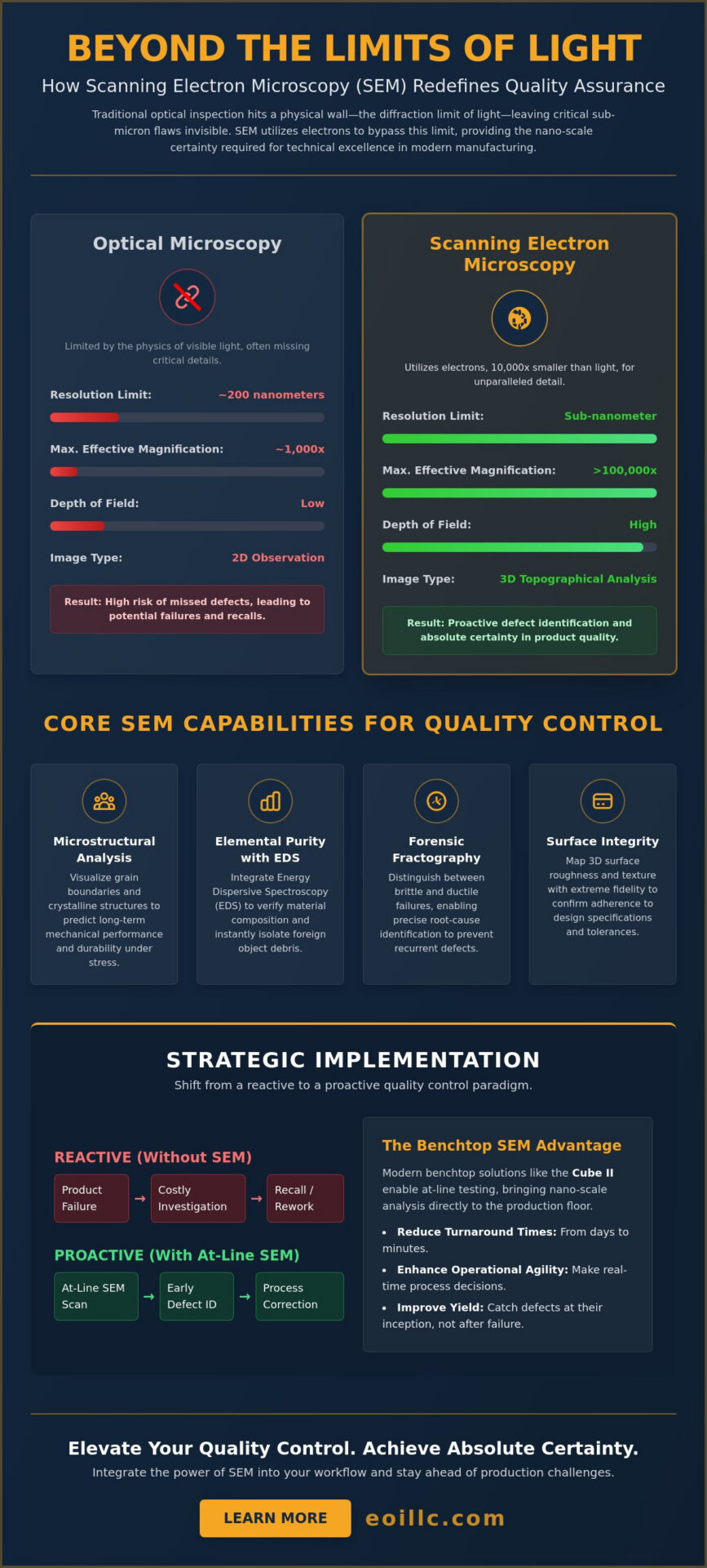
The fundamental limitation of traditional optical inspection lies in the physics of light itself. Visible light photons possess wavelengths ranging from approximately 400 to 700 nanometers, a physical constraint that dictates the maximum resolution achievable by even the most sophisticated lens systems. When industrial requirements demand the detection of defects smaller than half the wavelength of light, optical solutions inevitably fail. This is where the Scanning electron microscope (SEM) becomes indispensable. By utilizing a focused electron beam instead of photons, engineers bypass the diffraction limit, achieving resolutions that were previously unattainable. Understanding exactly how an sem improves product quality requires a shift in perspective from macro-scale viewing to nano-scale analysis. This transition from 2D observation to 3D morphological understanding is pivotal for modern quality assurance.
Resolution and Magnification: Seeing the Invisible
The primary mechanism behind how an sem improves product quality is its utilization of electron wavelengths, which are roughly 10,000 times shorter than those of visible light. This drastic reduction in wavelength allows for sub-micron resolution, enabling the identification of latent micro-cracks and structural discontinuities before they propagate into catastrophic failures. In high-performance manufacturing, verifying the integrity of surface finishes and thin-film coatings requires this level of precision. A minor adhesion failure at the nanoscale can compromise an entire component’s longevity. While optical tools struggle at 1,000x magnification, a desktop SEM maintains exceptional clarity at 100,000x. It’s this resolution gap that allows manufacturers to move beyond guesswork and achieve absolute certainty in their inspection protocols. It doesn’t just provide a larger image; it provides a more accurate representation of the material’s physical reality.
Topographical Analysis and Surface Integrity
Beyond simple magnification, the SEM provides a transformative advantage in depth of field. Traditional microscopes often struggle with 3D surfaces because only a narrow plane remains in focus at any given time. This makes it difficult to inspect components with significant vertical relief or complex textures. In contrast, SEM technology utilizes secondary electron imaging to create high-contrast maps of three-dimensional geometries. This capability is essential for inspecting machined parts or injection-molded components where manufacturing tolerances are measured in microns. Topographical analysis is defined as the systematic study of surface features and spatial arrangements to ensure strict adherence to manufacturing tolerances and design specifications. By mapping surface roughness and texture with extreme fidelity, engineers can confirm that every component meets the rigorous standards required for international distribution. It’s not just about seeing the surface; it’s about understanding the structural integrity of the material itself. This level of detail ensures that even the most minute deviations from the design intent are identified and corrected.
Microstructural Analysis: Detecting Sub-Micron Defects and Variability
Achieving superior industrial standards requires more than surface-level inspection; it necessitates a deep understanding of internal material architecture. This is precisely how an sem improves product quality by exposing the microstructural characteristics that dictate mechanical performance and long-term durability. In modern production quality control, the ability to visualize grain boundaries and crystalline orientations allows engineers to predict how a component will behave under high-stress conditions. Whether analyzing the complex lattices of a semiconductor wafer or the polymer chains in advanced composites, microstructural analysis provides a level of certainty that standard testing cannot match.
Grain Boundary and Crystalline Structure
The internal architecture of metals and ceramics isn’t uniform; it’s a complex network of crystalline grains whose size and orientation directly influence yield strength and fatigue resistance. An SEM allows for the precise characterization of these boundaries, revealing how thermal history and mechanical working have shaped the material. For instance, identifying heat treatment inconsistencies becomes a data-driven process when microstructural changes, such as unintended grain growth or phase precipitation, are clearly visible. By linking these crystalline orientations to macro-scale performance, manufacturers can optimize their processing parameters to ensure that every batch meets specific engineering requirements. It’s a level of meticulousness that transforms raw material verification into a strategic advantage.
Porosity and Inclusion Detection
Hidden defects like porosity and non-metallic inclusions are often the primary drivers of unexpected material failure. In cast components or parts produced through additive manufacturing, microscopic voids can act as stress concentrators, significantly reducing the part’s fatigue life. Detecting these sub-micron anomalies requires an understanding of the fundamental principles of scanning electron microscopy (SEM) in 2026, specifically how electron interactions with the sample volume reveal density variations. Non-metallic inclusions, which might be introduced during the melting or alloying process, are equally problematic. The SEM doesn’t just find these inclusions; it allows for the analysis of their morphology and distribution, providing the necessary data to refine upstream production processes.
Maintaining morphological consistency across raw material batches is a cornerstone of reliable large-scale production. When variability in particle size or shape is detected early in the supply chain, it prevents downstream assembly issues and reduces the risk of expensive product recalls. Technical teams looking to institutionalize these rigorous standards often evaluate advanced hardware like the Veritas Pro SEM to ensure consistent data across global facilities. By implementing these high-resolution analytical tools directly into the quality workflow, organizations move away from reactive troubleshooting and toward a visionary model of proactive reliability. This transition ensures that even the smallest microstructural deviation is addressed before it impacts the final product’s integrity.
Elemental Certainty: Leveraging EDS for Chemical and Purity Control
While topographical and microstructural analysis provide essential physical insights, achieving total quality assurance requires a rigorous evaluation of the chemical composition of the material. The integration of EDS (Energy Dispersive Spectroscopy) Systems into the inspection workflow represents a primary mechanism for how an sem improves product quality by providing real-time, quantitative elemental data. This spectroscopic capability allows for the instantaneous identification of atomic constituents within a sample, effectively transforming the SEM from a high-resolution imaging tool into a comprehensive analytical laboratory. By detecting the characteristic X-rays emitted during electron bombardment, engineers can verify that material recipes adhere strictly to design specifications, ensuring that no unauthorized substitutions or impurities have compromised the batch.
Identifying Contaminants and Impurities
Foreign object debris (FOD) and microscopic contaminants represent persistent threats to assembly line integrity, particularly in sectors where precision is non-negotiable. EDS distinguishes between intended materials and microscopic pollutants with exceptional clarity; for instance, it can differentiate between a stainless steel particle from a worn machine component and a silica grain introduced via the facility’s ventilation system. Tracing the source of contamination becomes a methodical process of identifying specific elemental signatures and comparing them against known environmental or process-related materials. This level of analytical rigor is vital for ensuring compliance with strict purity standards in the aerospace and medical device sectors, where even a single inclusion can lead to catastrophic failure. Verifying alloy compositions and coating thicknesses with stoichiometric precision ensures that materials perform as engineered under extreme operational stressors.
Chemical Mapping and Elemental Distribution
Beyond identifying the presence of specific elements, modern SEM systems enable the visualization of how these elements are spatially distributed across a sample surface. Chemical mapping provides a color-coded overlay that reveals the dispersion of dopants in semiconductor manufacturing or the distribution of reinforcing phases in a composite material. This spatial data is critical for verifying that chemical treatments, such as surface hardening or corrosion-resistant coatings, have been applied uniformly across the entire component geometry. EDS analysis provides a chemical “fingerprint” of the sample surface. By confirming the homogeneity of a material at the sub-micron level, manufacturers can guarantee consistent performance across large production volumes. This proactive approach to chemical verification reduces the reliance on destructive testing and reinforces the brand’s commitment to international standards of excellence. Data drives reliability; therefore, integrating chemical mapping into the standard QC protocol is a visionary step for any organization prioritizing technical authority.
Failure Analysis: Identifying Root Causes to Prevent Recurrent Defects
Systematic failure analysis represents the transition from reactive troubleshooting to proactive industrial evolution. By employing forensic engineering methodologies, organizations can transform a singular component failure into a comprehensive blueprint for structural optimization. This diagnostic rigor is a cornerstone of how an sem improves product quality, as it provides the empirical evidence required to bridge the gap between theoretical design and real-world performance. Rather than merely documenting a defect, high-resolution microscopy allows engineers to dissect the exact sequence of events that led to a material compromise. Data drives reliability. This proactive assessment is a primary example of how an sem improves product quality by identifying latent threats before they manifest in the field.
Fractography and Stress Analysis
Fractography serves as the primary tool for determining whether a failure resulted from a fundamental design flaw or an isolated manufacturing deviation. By examining fracture surfaces at high magnification, specialists can identify “beach marks” and microscopic striations that characterize fatigue failure over time. Distinguishing between brittle and ductile failure modes is essential for recalibrating production parameters. High-resolution imaging that pinpoints the exact site of crack initiation allows for the targeted reinforcement of high-stress zones. Utilizing failure analysis SEM techniques ensures that these insights are integrated back into the iterative product design cycle, preventing the recurrence of known vulnerabilities. It’s a methodical approach that ensures every failure contributes to a more robust future product.
Corrosion and Degradation Studies
Material degradation often begins at the sub-micron level, where localized chemical triggers initiate oxidation layers and microscopic pits. An SEM facilitates the detailed evaluation of these degradation sites, allowing quality teams to assess the effectiveness of protective coatings and chemical inhibitors. By analyzing the morphology of corrosion products, engineers can identify the specific environmental stressors responsible for the failure. This data-driven approach enables the selection of more resilient material grades, ensuring that products maintain their integrity in challenging operational environments. It’s a visionary strategy that prioritizes long-term reliability over short-term production speed. Identifying these triggers early prevents the widespread distribution of compromised hardware.
The ultimate goal of forensic analysis is the institutionalization of reliability across the entire manufacturing ecosystem. When every failure is treated as a learning opportunity supported by high-fidelity data, the brand’s reputation for excellence is reinforced. To implement these sophisticated diagnostic protocols within your own facility, explore the Veritas Series SEM for professional-grade failure analysis and root-cause identification.
Strategic Implementation: Improving Quality with Benchtop SEM Solutions
The historical paradigm of centralized laboratory testing is rapidly evolving into a model of decentralized, “at-line” inspection. This strategic shift is fundamental to how an sem improves product quality within modern high-throughput environments, as it eliminates the logistical delays associated with transporting samples to external facilities. By integrating advanced imaging directly into the production workflow, manufacturers achieve a rapid feedback loop that enables instantaneous process adjustments. The Cube II Benchtop SEM exemplifies this transition, offering a compact architecture that rivals the resolution of traditional floor-standing units while maintaining superior resistance to industrial vibrations. Reducing time-to-market through on-site sample characterization is no longer a luxury; it’s a competitive necessity for global innovators who prioritize technical agility.
The Advantages of Benchtop SEM in Production
Implementing a desktop SEM provides a significant return on investment by drastically reducing the costs of outsourced analysis and specialized laboratory infrastructure. These systems are engineered for ease of use, allowing skilled technicians to perform sophisticated sub-micron inspections without the extensive academic training traditionally required for electron optics. Their small footprint allows for seamless integration into existing quality control stations, ensuring that high-level analytical capabilities are always within reach of the assembly line. This accessibility ensures that how an sem improves product quality is through the democratization of high-precision data across the entire manufacturing team. The ability to verify tolerances in real-time ensures that deviations are corrected before they impact large production batches.
Ensuring Repeatability and Data Integrity
Data integrity is the anchor of any successful quality assurance program. Standardizing SEM operation ensures that measurements remain consistent across different shifts and operators, providing a stable baseline for longitudinal quality studies. Modern software suites further enhance this stability through automated routines for particle counting and defect recognition, which remove the subjectivity inherent in manual observation. This automation allows for the rapid generation of statistical reports that document compliance with international standards. However, the longevity of these precision instruments depends on a rigorous schedule of SEM maintenance. Preventative care ensures that instrument calibration remains within tolerance, guaranteeing that every data point generated is both accurate and repeatable. Reliability is not a static achievement but a continuous process of technical stewardship. By committing to regular preventative maintenance visits, organizations protect their analytical assets and ensure that their quality data remains beyond reproach.
Advancing Industrial Standards through Analytical Precision
The integration of scanning electron microscopy marks a definitive shift from visual estimation to empirical certainty. By bypassing the diffraction limits of visible light and utilizing energy-dispersive spectroscopy, organizations can now identify elemental contaminants and sub-micron structural defects with unprecedented accuracy. Understanding how an sem improves product quality is essential for maintaining global competitiveness in an era defined by stringent regulatory standards and complex material requirements. Whether through detailed fractography or at-line benchtop inspection, the transition to high-resolution analysis ensures that manufacturing tolerances are met and recurrent failures are eliminated.
While SEM provides the raw analytical data, managing this information across the entire product lifecycle is essential for true digital transformation. To understand how specialized consultancy can optimize your manufacturing data strategy, find out more.
As a seasoned innovator with over 30 years of electron microscopy expertise, we provide the technical infrastructure necessary to institutionalize these rigorous standards. As the authorized US distributor for EmCraft SEM systems, we offer comprehensive on-site training and robust service contracts to ensure your instrumentation delivers repeatable, high-fidelity data. Explore the Cube II Benchtop SEM for your Quality Control Lab to elevate your facility’s diagnostic capabilities. Embracing these advanced hardware solutions positions your organization at the forefront of industrial reliability and technical excellence.
Frequently Asked Questions
How does an SEM differ from an optical microscope in quality control?
SEM utilizes electron beams rather than visible light, which enables it to bypass the diffraction constraints that limit optical systems. This fundamental difference allows for significantly higher resolution and an expanded depth of field. Consequently, technicians can inspect complex topographical features and sub-micron defects that remain undetectable or blurred under standard light-based magnification.
Can a benchtop SEM provide enough resolution for advanced failure analysis?
Modern benchtop instruments, such as the Cube II, deliver high-resolution imaging that is entirely sufficient for the majority of industrial failure analysis requirements. These systems provide the clarity needed to identify fatigue striations and crystalline inclusions. While traditional floor-standing models offer higher peak magnifications, benchtop solutions provide an optimal balance of precision and accessibility for root-cause investigations.
What is the role of EDS in product quality assurance?
EDS integration is a primary factor in how an sem improves product quality by providing real-time elemental characterization of the sample surface. This capability allows quality teams to verify alloy stoichiometry and identify the specific chemical signatures of foreign object debris. By transforming a visual image into a quantitative chemical map, EDS ensures that material purity meets strict design specifications.
How much time can an on-site SEM save in a typical manufacturing workflow?
Integrating an SEM directly into the manufacturing workflow can reduce analysis lead times from several days to under an hour. By eliminating the logistical delays associated with third-party testing laboratories, technical teams can perform “at-line” inspections. This rapid feedback loop allows for immediate corrections to production parameters, significantly reducing the risk of manufacturing large volumes of defective hardware.
Is specialized training required to operate a modern benchtop SEM like the Cube II?
Modern benchtop SEMs are engineered for operational efficiency, featuring streamlined interfaces that don’t require an advanced degree for standard use. While foundational training is necessary to optimize image quality and sample preparation, automated software routines handle many complex alignment tasks. Most technicians can become proficient in routine quality checks following a comprehensive on-site training program.
What industries benefit most from integrating SEM into their QC process?
High-stakes industrial sectors, including aerospace, semiconductor manufacturing, and medical device production, derive the greatest strategic value from SEM integration. These industries operate under rigorous tolerances where microscopic inclusions or coating delamination can lead to catastrophic failure. Metallurgy and polymer science also rely heavily on electron microscopy to characterize grain structures and verify material homogeneity across global supply chains.
How does SEM help in meeting international quality standards like ISO or ASTM?
The implementation of electron microscopy is a fundamental way how an sem improves product quality by generating the empirical data required for ISO and ASTM compliance. SEM technology provides the high-fidelity measurements necessary to satisfy the documentation requirements of ISO 16700 and various metallurgical protocols. This level of analytical rigor is often mandatory for organizations seeking to maintain professional certifications in specialized technical fields.
Can SEM be used to analyze non-conductive materials for quality issues?
Non-conductive samples, such as polymers and ceramics, can be successfully analyzed using specialized techniques like low-vacuum imaging or sputter coating. Applying a nanometer-thin layer of a conductive material like gold prevents the accumulation of static charge on the sample surface. This ensures that the electron beam can resolve fine details without the image distortion typically associated with non-metallic materials.