

Relying on factory-default settings for high-precision metrology is a gamble that compromises the integrity of an entire analytical workflow. Many laboratory managers struggle with persistent image drift and the increasing complexity of meeting ISO 16700:2016 or internal audit requirements. Mastering how to calibrate a scanning electron microscope is no longer a peripheral skill; it’s a fundamental necessity for ensuring traceable magnification accuracy. You’ve likely encountered the confusion between routine stigmation correction and formal calibration protocols, yet these processes remain distinct pillars of instrument performance.
This technical guide outlines the rigorous methodology required to achieve peak analytical performance and extend the intervals between professional service visits. We’ll explore the integration of the latest NIST DTSA-II software, codenamed Kelvin, alongside established ASTM E766-14e1 standards. By the end of this article, you’ll possess a repeatable protocol that provides absolute confidence in your measurement data. This systematic approach transforms your SEM from a simple imaging tool into a robust, metrologically sound system capable of meeting the sophisticated demands of 2026 industrial standards.
Key Takeaways
- Establish a clear distinction between magnification verification and full system calibration to maintain the highest standards of metrological traceability in your laboratory.
- Identify the most effective calibration standards, from pitch to particle size, and learn to select the optimal tool for your specific magnification range.
- Implement a rigorous step-by-step protocol for how to calibrate a scanning electron microscope, focusing on the meticulous alignment of electron optics for superior data integrity.
- Recognize the early indicators of calibration drift to proactively maintain compliance with ISO requirements and internal quality audits.
- Leverage advanced automated routines within systems like the Cube II and Genesis series to streamline calibration workflows and minimize the necessity for manual intervention.
The Fundamentals of SEM Calibration and Metrological Traceability
The operation of a Scanning Electron Microscope (SEM) relies on the precise correlation between the electronic scan signal and the physical dimensions of the specimen surface. Calibration is the rigorous process of establishing this correlation to ensure that the digital representation on the monitor accurately reflects the actual scale of the microstructures being analyzed. It’s a common misconception that high-resolution imaging alone suffices for technical reporting. In reality, the integrity of your data depends on how to calibrate a scanning electron microscope through a systematic comparison against a known physical standard.
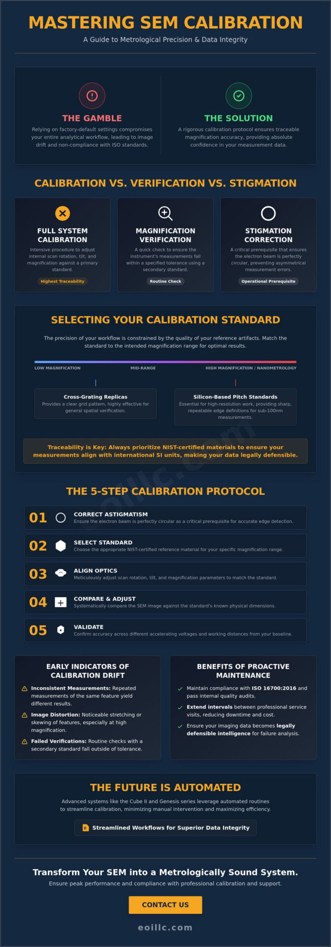
Distinguishing between magnification verification and full system calibration is vital for laboratory compliance. Verification involves a cursory check to ensure the instrument’s measurements fall within a specified tolerance, often using a secondary standard. Full calibration is a more intensive procedure that adjusts the internal scan rotation, tilt, and magnification parameters to align the instrument with primary reference data. This process is sensitive to fluctuations in accelerating voltage and working distance. Even minor deviations in the electromagnetic lens current can alter the beam’s landing position, necessitating a recalibration if the operational parameters shift significantly from the calibrated baseline.
Why Traceability Matters in 2026
In modern industrial sectors, the chain of comparison back to international SI units is the only way to guarantee measurement confidence. Using NIST-certified materials provides a transparent lineage of accuracy that is indispensable for semiconductor manufacturing and advanced materials science. This alignment represents a transformation of raw imaging data into legally defensible intelligence. Without this traceability, industrial failure analysis lacks the evidentiary weight required for legal or regulatory scrutiny. Accurate calibration prevents the costly errors that occur when subtle structural deviations are misidentified, supporting the synergy between ecological responsibility through waste reduction and superior industrial precision.
Calibration vs. Stigmation Correction
Technical operators often confuse stigmation correction with the broader scope of instrument calibration. Correcting astigmatism is a critical prerequisite, as it ensures the electron beam maintains a circular symmetry. If the beam is distorted into an ellipse, the precision of edge detection during the calibration process is compromised, leading to asymmetrical measurement errors. While users can often manage stigmation and basic magnification checks, a comprehensive protocol for how to calibrate a scanning electron microscope often reveals when a system requires the expertise of a professional field service engineer to resolve deeper hardware instabilities or electronic noise issues.
Essential Tools and Standards for Accurate Calibration
The precision of a metrological workflow is fundamentally constrained by the quality of the physical artifacts employed as references. Achieving a high degree of accuracy when learning how to calibrate a scanning electron microscope involves selecting standards that are appropriate for the specific magnification regime of the analysis. These standards, which include pitch, grid, and particle size references, act as the physical anchor for the electronic scan system. Without a traceable artifact, any measurement remains a relative estimation rather than an absolute value. Industrial leaders prioritize standards that come with a certificate of traceability, ensuring that every micron measured in the lab aligns with international benchmarks.
Selecting Your Calibration Reference Material
Understanding how to calibrate a scanning electron microscope effectively requires matching the reference standard to the intended magnification range. Cross-grating replicas are highly effective for low to mid-range magnification calibration, providing a clear grid pattern for general spatial verification. For high-resolution nanometrology, silicon-based pitch standards are essential. These standards utilize the crystalline structure of silicon to provide extremely sharp, repeatable edge definitions required for sub-100nm measurements. The NIST procedure for SEM calibration highlights that the uncertainty of the reference material is a primary component of the total measurement uncertainty. For resolution testing and stigmation correction, gold-on-carbon standards are the preferred choice. The high-contrast gold islands on a dark carbon background allow for the precise beam shaping necessary before any formal calibration begins.
Environmental and Hardware Pre-requisites
Hardware stability is a prerequisite for any meaningful calibration. Standards must be mounted on specialized low-outgassing stubs to prevent hydrocarbon contamination from accumulating under the electron beam. Such contamination can cause charging or physical buildup that alters the perceived dimensions of the standard. Environmental factors are equally critical. Vibration isolation systems must be active, and electromagnetic interference shielding should be verified to prevent beam deflection. Before beginning the procedure, ensure the electron gun is fully saturated and the beam is centered. Stage stability must also be confirmed; even a few nanometers of mechanical drift during the capture cycle will result in skewed data. For laboratories that demand absolute reliability, scheduling regular preventative maintenance visits ensures that the vacuum systems and electronic components remain within peak operational tolerances, providing a stable foundation for all subsequent metrological tasks.
Step-by-Step Procedure for SEM Magnification Calibration
Executing a precise calibration requires more than just high-quality artifacts; it demands a methodical approach to instrument stabilization and optical alignment. While modern software interfaces often promise simplified solutions, true metrological integrity is only achieved through a unified procedural checklist that validates every stage of the imaging chain. Understanding how to calibrate a scanning electron microscope involves a deep familiarity with the interplay between the electron beam and the digital-to-analog converters that drive the scan coils. A disciplined workflow ensures that spatial measurements remain consistent across various operational shifts and user groups.
Primary Calibration Workflow
The procedure begins by loading the NIST-traceable standard into the vacuum chamber and achieving the optimal working distance, which is typically specified by the manufacturer to minimize lens aberrations. Once the vacuum levels stabilize, you must saturate the electron gun and perform fine focus and stigmation correction at a magnification significantly higher than the target calibration point. For example, if you’re calibrating at 10,000x, you should refine the beam at 50,000x to ensure the probe size is optimized. Capture high-contrast images at specific intervals, such as 1,000x, 10,000x, and 50,000x. This multi-scale approach allows you to check the linearity of the scan amplifiers and ensures that the magnification remains accurate across the instrument’s entire operational range.
Calculating and Applying Correction Factors
After capturing the reference images, use the integrated measurement software to correlate the pixel counts with the known physical dimensions of the standard. It’s critical to measure features in both the X and Y axes to identify potential scan distortion or non-orthogonality. These distortions often arise from electronic drift or minor instabilities in the electromagnetic scan coils. Input the measured values into the SEM software’s calibration utility to update the internal scaling factors. This step directly adjusts the scale bar displayed on all future micrographs. You must then re-verify the measurements against the standard to confirm that the correction was successful and falls within the required tolerance levels.
Finalizing the process requires meticulous documentation for the laboratory’s quality management system. Every calibration event should be recorded with the date, accelerating voltage, working distance, and the specific serial number of the NIST-traceable standard used. This creates a transparent audit trail that is essential for maintaining ISO compliance and providing measurement confidence in industrial failure analysis. By following this systematic protocol for how to calibrate a scanning electron microscope, laboratories can ensure that their data is not only visually impressive but also metrologically sound and legally defensible.
The necessity for such legally defensible data is not limited to the lab; in the world of property management, professionals often learn more about 1ESX Roof & Wall Reports to obtain the same level of certified accuracy for structural measurements.
Maintaining Compliance: Frequency and Troubleshooting
The cadence of metrological verification is not a static variable but a function of instrument duty cycles and the stringency of the regulatory environment. High-utilization laboratories in specialized industrial sectors often implement quarterly or even monthly checks to ensure that their data remains beyond reproach. Establishing a recommended calibration schedule requires a balance between operational efficiency and the necessity for absolute measurement confidence. While modern systems are designed for stability, the intersection of mechanical wear and electronic drift necessitates a disciplined approach to monitoring how to calibrate a scanning electron microscope within a formalized quality management system.
Signs of Calibration Drift
Subtle erosions in measurement accuracy often manifest as image stretching, where the scaling factors in the X and Y axes diverge over time. This non-linear scaling across the field of view is a primary indicator that the scan amplifiers or the digital-to-analog converters require adjustment. Operators must also remain vigilant for inconsistencies between secondary electron imaging and EDS mapping; a spatial mismatch between a morphological feature and its elemental signature typically points to a loss of calibration integrity. Additionally, every filament change or aperture adjustment disrupts the electron optical column’s equilibrium. These routine events should trigger a review of the system’s alignment to determine if a full recalibration is required to restore the baseline performance standards established during the previous certification cycle.
Regulatory Standards and Documentation
Passing a technical laboratory audit, such as those governed by ISO 17025, requires more than just accurate hardware. It demands a meticulous audit trail consisting of calibration certificates, uncertainty budgets, and detailed SEM maintenance records. These logs act as the foundational evidence of a laboratory’s commitment to metrological stability and international capability. In the context of industrial failure analysis, the legal and safety implications of inaccurate measurements are profound. A single miscalibrated micron could lead to the misidentification of a structural defect or a material impurity, potentially resulting in catastrophic system failure. Interpreting calibration certificates for these audits involves a detailed analysis of the reported uncertainty and the environmental conditions present during the testing phase, ensuring the chain of comparison to SI units remains unbroken.
Preventative maintenance acts as a proactive safeguard, extending the longevity of calibration settings by addressing mechanical instabilities in the stage and potential electronic noise in the scan generators before they degrade the signal quality. To ensure your instrumentation remains compliant with these rigorous international standards and continues to deliver peak analytical performance, you can book a professional preventative maintenance visit to secure your system’s long-term stability and precision.
Professional Calibration and Advanced SEM Support
Distinguishing between routine user-level adjustments and the specialized expertise of professional field service engineering is essential for maintaining an elite analytical infrastructure. While laboratory staff can master how to calibrate a scanning electron microscope for daily verification, certain deep-system optimizations require the diagnostic tools and technical authority of a seasoned engineer. The integration of EDS Systems calibration with standard magnification protocols represents a critical synergy, ensuring that morphological data and elemental mapping are perfectly synchronized. This alignment is a prerequisite for advanced failure analysis where the accuracy of chemical distribution is as vital as the precision of the physical dimensions. Relying on professional support ensures that your instrument’s internal scan rotation, tilt, and magnification parameters are aligned with the highest international standards.
The Role of Modern Benchtop SEM Software
The Cube II Benchtop SEM and the Genesis Tabletop SEM represent a significant evolution in how to calibrate a scanning electron microscope through the use of sophisticated automated software routines. These systems utilize intuitive user interfaces that reduce the complexity of metrological tasks, allowing for rapid verification tools that maintain traceable accuracy between formal service intervals. For more demanding environments, the Veritas Series SEM, specifically the Veritas HR SEM and Veritas FE SEM models, offers enhanced stability and high-resolution calibration capabilities that push the boundaries of what’s possible in a compact footprint. These automated routines don’t just save time; they eliminate the variability inherent in manual pixel counting, providing a steady, expert-driven narrative of data integrity that’s essential for B2B partners who value depth and expertise.
When to Seek Expert Field Service
Identifying the threshold where internal adjustments fail is a hallmark of an expert operator. Critical hardware failures, such as aperture degradation or electromagnetic coil drift, often manifest as persistent calibration errors that require physical intervention. Even the most advanced Veritas Pro or Veritas Ultra SEM units require the meticulous attention of a specialist to resolve underlying electronic noise or vacuum instabilities. Investing in comprehensive SEM operation training empowers your team to recognize these early indicators, maximizing equipment uptime and long-term accuracy. An annual service contract ensures that your instrument receives the rigorous maintenance required for guaranteed metrological precision. This proactive approach to system health reinforces your laboratory’s status as a reliable partner in global industrial production, ensuring that your internal processes are as rigorous as the international standards you aim to uphold.
Ultimately, the goal of professional calibration is to transform your hardware from a standalone imaging device into a metrologically sound component of a larger corporate strategy. By combining high-end consumables, such as specialized filaments, with regular preventative maintenance visits, you ensure that the system’s performance remains consistent over years of heavy use. This methodical approach to technical integration provides the stability and thoroughness required for large-scale production and logistical excellence, keeping your laboratory at the intersection of innovation and reliability.
Advancing Metrological Excellence in Scanning Electron Microscopy
The transition from qualitative imaging to quantitative metrology requires a steadfast commitment to traceability and systematic protocol. We’ve explored how the integration of NIST-certified standards and rigorous alignment procedures ensures that your laboratory data stands up to the most demanding industrial audits. Mastering how to calibrate a scanning electron microscope is the first step in establishing a stable analytical environment where measurement confidence is guaranteed. While user-level verification is essential for daily operations, long-term precision relies on the intersection of advanced software routines and professional hardware maintenance.
Electron Optics Instruments leverages over 30 years of industry expertise to support your technical objectives, serving as the sole US distributor for EmCraft SEMs while providing comprehensive service for all major SEM brands. This depth of experience ensures that your equipment remains a reliable anchor for industrial innovation and failure analysis. Ensure your SEM precision with expert training and service from Electron Optics Instruments. By aligning your internal workflows with these high standards, you’ll secure the accuracy required for the next generation of materials science.
Frequently Asked Questions
How often should a scanning electron microscope be calibrated?
Calibration frequency is dictated by the specific duty cycle of the instrument and the stringency of the laboratory’s internal quality standards. While high-utilization industrial facilities often mandate quarterly metrological assessments, many research environments find semi-annual schedules sufficient to maintain compliance. It’s critical to perform a full calibration after any major hardware modification, such as a filament replacement or lens cleaning, to ensure the imaging system remains within documented tolerances.
What is the difference between calibration and verification in SEM?
Calibration is the formal process of adjusting the instrument’s internal scan parameters to align with a traceable physical standard. Verification, conversely, involves a periodic check to confirm that the SEM’s current performance remains within specified operational limits without making permanent adjustments to the software scaling. Verification acts as a proactive safeguard between scheduled calibration events to ensure ongoing data integrity and metrological stability.
Do benchtop SEMs like the Cube II require different calibration tools than floor models?
Benchtop systems like the Cube II Benchtop SEM utilize the same fundamental NIST-traceable artifacts, such as silicon-based pitch standards or cross-grating replicas, as their floor-standing counterparts. The primary difference lies in the integration of automated software routines that simplify the user-level verification process. Regardless of the instrument’s footprint, the necessity for a high-quality physical reference remains constant to achieve traceable magnification accuracy and peak analytical performance.
Can I use any grid for SEM magnification calibration?
Utilizing a non-traceable grid for formal calibration is insufficient for industrial compliance or peer-reviewed publication. While a standard copper mesh might assist in cursory magnification checks, it lacks the certified dimensional accuracy required for metrological traceability. Effective protocols for how to calibrate a scanning electron microscope demand the use of artifacts with a documented chain of comparison to international SI units, ensuring that every measurement is legally and scientifically defensible.
What environmental factors most commonly cause an SEM to lose calibration?
Thermal fluctuations and mechanical vibrations are the most frequent catalysts for calibration drift in high-resolution systems. Significant changes in ambient laboratory temperature can cause the electromagnetic lenses to expand or contract slightly, altering the focal length and magnification. Additionally, stray electromagnetic interference (EMI) from nearby heavy machinery or unshielded power cables can deflect the electron beam, introducing subtle scan distortions that compromise the precision of the calibrated scale bar.
Is NIST traceability required for all SEM applications?
NIST traceability is not a universal requirement for every imaging task, yet it’s mandatory for regulated industries like semiconductor manufacturing and forensic failure analysis. For general morphological surveys where absolute dimensional accuracy is secondary to visual detail, a non-traceable standard may suffice. However, establishing traceability is a hallmark of professional metrology and provides a layer of institutional security that protects the integrity of long-term research and industrial production.
How does stigmation affect the accuracy of my SEM measurements?
Proper stigmation correction is a vital prerequisite because an astigmatic beam creates an elliptical probe that distorts the edges of the features being measured. If the beam is not perfectly circular, the pixel counts in the X and Y axes will reflect a distorted geometry rather than the actual physical dimensions of the specimen. Ensuring beam symmetry through meticulous stigmation is essential for the precise edge detection required when learning how to calibrate a scanning electron microscope accurately.
What should I do if my SEM fails to hold its calibration settings?
Persistent failure to maintain calibration often indicates an underlying hardware instability, such as a degrading aperture or a failing scan generator. You should first verify the vacuum levels and ensure the environmental shielding remains intact to rule out external interference. If the drift persists despite these checks, it’s necessary to consult a professional field service engineer to diagnose deeper electronic noise or mechanical wear within the electron optical column.