The persistent glow or unpredictable streaking across a high-resolution micrograph is rarely a sign of hardware failure; instead, it’s a fundamental breakdown in the delicate equilibrium of electron flux. For researchers and quality control engineers, these artifacts represent more than just aesthetic flaws. They are a significant barrier to reliable data acquisition that can derail critical project timelines. If you’ve ever questioned whether your sample preparation or your vacuum system is at fault, you’re grappling with a common but complex technical challenge. Understanding how to fix sem charging issues requires a shift from trial-and-error adjustments toward a methodical mastery of beam physics and surface conductivity.
This guide provides a professional framework for mitigating electron accumulation by integrating established coating protocols with modern 2026 hardware capabilities. You’ll learn how to leverage precise accelerating voltage reductions and advanced detector settings to restore absolute image clarity. We will examine a multi-layered mitigation strategy that spans from the initial deposition of 2 to 10 nm conductive layers to the sophisticated use of variable pressure modes found in high-performance systems like the Veritas Series or Cube II. By the end of this analysis, you’ll possess the technical authority to eliminate artifacts and ensure your scanning electron microscopy workflows remain both rigorous and efficient.
Key Takeaways
- Analyze the “Charge Balance” equation to determine the precise physical cause of electron accumulation on non-conductive surfaces.
- Execute immediate operational adjustments, including the reduction of accelerating voltage and beam current, to learn how to fix sem charging issues at the source.
- Apply professional-grade sputter coating and conductive grounding techniques to ensure a reliable path for electron dissipation.
- Utilize Variable Pressure and Low Vacuum hardware modes to neutralize surface charges through controlled gas ionization within the chamber.
- Identify how regular preventative maintenance and aperture calibration prevent systemic beam instability and persistent imaging artifacts.
Understanding the Mechanism of SEM Charging
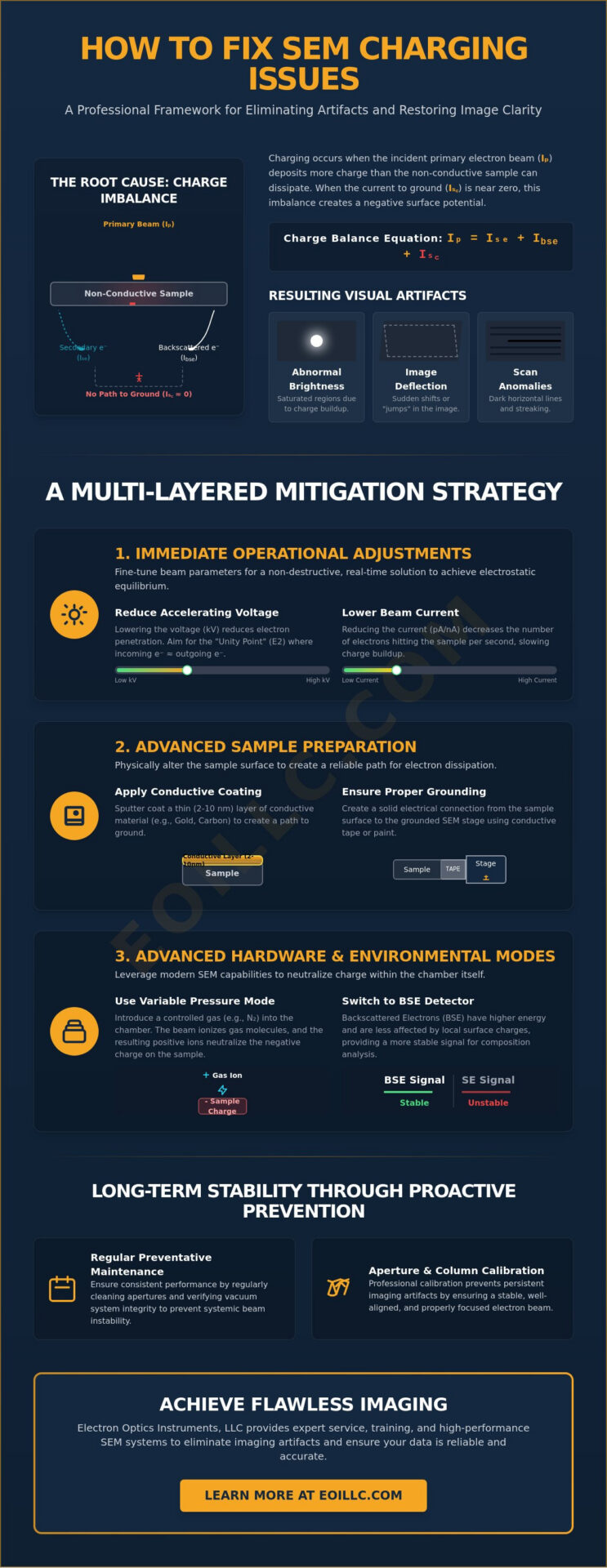
Specimen charging within a scanning electron microscope is a fundamental physical phenomenon where the incident primary electron beam deposits more charge than the sample can effectively dissipate. This localized accumulation of negative electrostatic potential occurs primarily when the specimen lacks sufficient electrical conductivity to facilitate a path to ground. For researchers and laboratory managers seeking how to fix sem charging issues, it’s essential to recognize that this is not a hardware malfunction but a dynamic imbalance of electron flux. When the rate of incoming electrons exceeds the combined rate of secondary electron emission, backscattered electron emission, and specimen current to ground, the surface potential begins to shift unpredictably.
The “Charge Balance” equation provides the mathematical framework for this interaction, defined as Ip = Ise + Ibse + Isc. In this relationship, Ip represents the primary beam current, while Ise and Ibse denote the current from secondary and backscattered electrons, respectively. The variable Isc signifies the specimen current flowing to ground. In conductive materials, this system maintains equilibrium effortlessly. However, in insulating specimens, Isc approaches zero, causing the sample to act as a capacitor. This storage of electrons results in several distinctive visual artifacts that compromise data integrity:
- Abnormal Brightness: Intense, saturated regions where the negative surface potential accelerates secondary electrons toward the detector.
- Image Deflection: Sudden shifts or “jumps” in the field of view as the accumulated charge repels the primary beam.
- Scanning Anomalies: Dark horizontal lines or “streaking” caused by unstable emission during the raster process.
Achieving technical proficiency in how to fix sem charging issues starts with distinguishing between surface charging and internal “trapped” charge. While surface charging affects immediate topographical resolution, trapped charges often occur within porous ceramics or complex polymers. These electrons migrate into the sub-surface matrix, creating a persistent internal electric field that can influence the beam even after surface-level mitigation has been attempted.
The Role of Secondary and Backscattered Electrons
Secondary electron (SE) yield is highly sensitive to the accelerating voltage of the primary beam. At a specific energy known as the “Unity Point” or E2, the total number of outgoing electrons exactly equals the number of incident electrons, resulting in a net charge of zero. Operating near this equilibrium point is a sophisticated strategy for imaging non-conductive surfaces. In contrast, backscattered electrons (BSE) possess higher kinetic energy and are significantly less influenced by the localized electric fields generated by surface charging, making BSE detectors a reliable alternative for compositional analysis on challenging samples.
Why Insulating Materials Pose the Greatest Challenge
Polymers, high-purity ceramics, and biological specimens lack the free electrons necessary for rapid charge dissipation. When the electron beam strikes these insulating surfaces, it creates a localized negative field that acts as a virtual electrode. This field doesn’t just distort the current scan; it actively deflects subsequent electrons in the raster pattern. Without a deliberate intervention, such as sputter coating or environmental vacuum control, the resulting image artifacts render the data unusable for professional engineering or forensic applications.
Immediate Operational Adjustments to Mitigate Charging
When immediate intervention is required to stabilize a micrograph, the operator must prioritize a systematic hierarchy of beam parameter adjustments. This technical sequence provides a non-destructive method for achieving electrostatic equilibrium without altering the specimen’s physical state. Mastering how to fix sem charging issues requires a granular understanding of how electron flux interacts with the sample surface in real-time. By manipulating the primary beam’s energy and delivery rate, professionals can often mitigate artifacts before resorting to more intensive sample preparation or hardware modifications.
Optimizing Accelerating Voltage (kV)
For uncoated, non-conductive specimens, reducing the accelerating voltage to a range of 1-5 kV is often the most effective initial step. This reduction aims to reach the E2 unity point, where the total secondary and backscattered electron yield equals the primary beam current. While lower voltages significantly reduce charge accumulation, they present a known trade-off with spatial resolution due to increased chromatic aberration and a larger interaction volume at the surface. Most industrial polymers achieve charge stability within the 0.8 to 2.0 kV range. Professional systems, such as the Veritas FE SEM, offer the precision control necessary to navigate these low-voltage regimes while maintaining superior imaging standards.
Strategic Scan Rate Selection
The temporal distribution of electrons is as critical as their energy levels. Increasing the scan speed to a TV rate or faster prevents the electron beam from dwelling on a single coordinate long enough to establish a localized electric field. This high-speed raster pattern allows the accumulated charge to dissipate across a wider area, reducing the severity of Image artefacts and trouble-shooting challenges. To ensure data integrity, the following operational modes should be utilized:
- Reduced Area Mode: Use this function to focus and align the beam on a localized region, minimizing the total electron dose to the surrounding field of view before capturing the final image.
- Spot Mode: High-precision focusing should be performed rapidly to avoid “burning” or permanently charging the specific area of interest.
- Frame Averaging and Integration: To compensate for the reduced signal-to-noise ratio inherent in high-speed, low-current imaging, utilize frame averaging. This process mathematically combines multiple fast scans to produce a single, clear image without the artifacts associated with slow-scan dwell times.
Lowering the beam current, often referred to as adjusting the spot size, is the final pillar of this operational triad. By decreasing the number of electrons arriving at the surface per unit of time, the rate of charge buildup is drastically slowed. When combined with methodical scan rate adjustments and frame integration, these parameters form a robust protocol for any laboratory seeking how to fix sem charging issues during critical research or quality control cycles.
Advanced Sample Preparation and Grounding Techniques
While operational adjustments provide a non-destructive first line of defense, achieving long-term stability on highly insulating materials often requires physical modification of the specimen’s electrical properties. Advanced sample preparation techniques represent the most reliable methodology for researchers seeking how to fix sem charging issues in high-resolution workflows. By establishing a robust conductive network across the specimen surface, you can ensure that incident electrons find a rapid path to ground, effectively neutralizing the electrostatic potential before it compromises image clarity.
Sputter Coating Best Practices
Sputter coating is the deposition of a nanometer-scale conductive layer via plasma discharge. This process involves bombarding a target material, such as gold or platinum, with ionized gas to release atoms that settle uniformly on the sample surface. For general imaging applications, a gold coating provides excellent secondary electron emission, though its grain size can occasionally obscure sub-nanometer features at extreme magnifications. Platinum or palladium are preferred for high-resolution applications due to their significantly finer grain structure. Operators must maintain a precise coating thickness between 5 and 20 nm; layers thinner than 5 nm may fail to provide a continuous conductive path, while layers exceeding 20 nm risk masking delicate topographical details and altering the specimen’s authentic morphology.
Ensuring a Solid Path to Ground
Even a perfectly coated sample will exhibit artifacts if the interface between the specimen and the mounting stub is compromised. Utilizing conductive adhesives, such as double-sided carbon tape or silver dag, is essential for creating a low-resistance connection. The “Carbon Bridge” technique is particularly effective for complex specimens; it involves applying a small strip of conductive tape or a drop of silver paint from the top of the sample directly to the aluminum stub. This bypasses the bulk resistance of the material and provides a direct exit for accumulated electrons. Adhering to SEM operation best practices also includes the meticulous cleaning of sample holders and the SEM stage. Residual insulating oils from handling can act as dielectric barriers, frustrating even the most rigorous grounding efforts.
Sample geometry plays a decisive role in charge distribution. Flat, planar surfaces allow for uniform coating and predictable electron emission, whereas complex 3D structures often contain recessed features or “shadowed” areas that remain uncoated during the sputtering process. These internal cavities act as charge traps, creating localized electric fields that distort the primary beam. When analyzing high-aspect-ratio samples, it’s often necessary to utilize rotational sputtering or tilt the sample during preparation to ensure every surface is integrated into the conductive network. By addressing these physical variables, you can eliminate the root cause of image artifacts and ensure consistent data acquisition across diverse material types.
Hardware Solutions: Variable Pressure and Environmental Control
Advanced hardware integration offers a decisive alternative to physical specimen modification by manipulating the imaging environment itself. Variable Pressure (VP) or Low Vacuum (LV) modes represent a pinnacle of technical innovation for laboratories seeking how to fix sem charging issues without the need for conductive coatings. This approach is particularly advantageous for forensic analysis, polymer research, and biological studies where maintaining the sample’s pristine state is paramount. By introducing a controlled amount of gas into the specimen chamber, the system creates a self-neutralizing environment that stabilizes the electrostatic potential in real-time, allowing for high-fidelity data acquisition on specimens that would otherwise remain unusable.
The Physics of Low-Vacuum Imaging
The mechanism of charge neutralization in a low-vacuum environment relies on the interaction between the primary electron beam and residual gas molecules. As the beam passes through the chamber, it ionizes the gas, creating a cloud of positive ions. These ions are naturally attracted to the negative surface charge accumulating on the specimen, effectively canceling the charge before it can distort the beam. Achieving this equilibrium typically requires pressure ranges between 10 and 100 Pa, depending on the material’s dielectric properties. The Cube II Benchtop SEM stands as a leader in this category, providing a streamlined interface for managing these complex pressure variables while maintaining the resolution typically reserved for larger floor-model systems. It’s a system designed for rapid deployment in industrial settings where speed and accuracy are non-negotiable.
Specialized Detectors for Charging Samples
Standard Secondary Electron (SE) detectors often struggle in high-pressure or charging environments because the localized electric fields easily deflect low-energy electrons. To overcome this, professional workflows prioritize specialized detection hardware:
- Backscattered Electron (BSE) Detectors: Because backscattered electrons possess significantly higher kinetic energy, they’re less susceptible to the influence of surface charging. This makes them superior for compositional analysis on insulating materials.
- Gaseous Secondary Electron Detectors (GSED): Specifically engineered for environmental SEM (ESEM) applications, these detectors utilize the gas ionization process to amplify the signal, providing clear topographical data even on wet or outgassing samples.
- In-Lens Detectors: These are critical for low-voltage imaging, capturing electrons within the column to minimize the impact of external surface potentials.
The transition toward these hardware-centric solutions reflects a broader industry movement toward efficiency and technical synergy. If your current workflows are limited by persistent artifacts, you can explore the Veritas Series SEM to see how integrated environmental controls revolutionize imaging precision. By shifting the burden of charge mitigation from the operator to the instrument’s internal systems, you ensure a more reliable and repeatable analytical process. Understanding how to fix sem charging issues through hardware automation doesn’t just improve image quality; it fundamentally transforms the throughput of your specialized industrial operations.
Eliminating Charging Through Professional Service and Training
The resolution of persistent image artifacts extends beyond the immediate manipulation of beam physics or specimen preparation. While the operator’s skill in adjusting kV and scan rates is vital, the physical condition of the electron column itself plays a silent but decisive role in image stability. Determining how to fix sem charging issues often necessitates a critical evaluation of the instrument’s internal cleanliness and vacuum integrity. When a system’s internal components are compromised, even the most rigorous sample preparation cannot compensate for the resulting beam instability. Achieving a truly artifact-free environment requires a holistic commitment to hardware excellence and standardized operational protocols.
Preventative Maintenance and System Cleanliness
Hydrocarbon contamination within the vacuum chamber is a primary, yet frequently overlooked, catalyst for pseudo-charging artifacts. These organic residues often originate from improper sample handling or the gradual breakdown of vacuum pump oils. When the electron beam interacts with these molecules, they polymerize on the surfaces of the final aperture and the lower pole piece. This creates a thin insulating layer that accumulates charge just like a non-conductive specimen would. This “column charging” deflects the primary beam, causing drift and astigmatism that mimics the appearance of specimen-level charging. Regular aperture cleaning and the replacement of consumables are fundamental to maintaining a “clean” beam path. For a comprehensive overview of these protocols, refer to our definitive guide to SEM maintenance to ensure your system operates at peak theoretical performance.
Standardizing Lab Workflows
Technical authority in microscopy is built upon the foundation of repeatable processes. Individual variation in how operators approach challenging samples can lead to inconsistent data and delayed project timelines. Establishing rigorous Standard Operating Procedures (SOPs) for non-conductive materials ensures that every team member utilizes the most effective mitigation strategies. On-site professional training bridges the gap between theoretical beam physics and the practical realities of industrial imaging. These sessions empower staff to identify whether a specific artifact is a result of sample preparation, operational settings, or a systemic hardware failure.
Aperture health is paramount. If your laboratory continues to struggle with unpredictable image shifts despite following established protocols, the issue likely resides within the column’s internal geometry. Establishing a structured maintenance schedule is the most effective way to address these persistent hardware-related imaging issues before they result in significant downtime. You can explore our SEM service contracts to ensure your lab maintains peak imaging performance through regular preventative maintenance visits. By integrating professional service with advanced operator training, you create a robust analytical environment where the primary focus remains on discovery and quality control rather than troubleshooting technical failures. Mastering how to fix sem charging issues is ultimately a synergy of meticulous hardware care and expert-driven methodology.
Advancing Imaging Precision Through Technical Mastery
Mastering the complexities of electron-specimen interactions is essential for maintaining the integrity of specialized industrial research. This guide has detailed various methodologies on how to fix sem charging issues through a multi-faceted approach, ranging from the immediate optimization of beam parameters to the implementation of advanced environmental controls. By balancing surface conductivity with environmental vacuum pressures, laboratories can transcend the limitations of insulating materials and achieve consistent, high-resolution results. These strategies ensure that data acquisition remains precise, even when dealing with the most challenging non-conductive specimens in 2026.
Ensuring your instrumentation remains at peak performance requires more than just operational knowledge; it demands a partnership with seasoned industry experts. Electron Optics Instruments, LLC brings over 30 years of industry expertise as the sole US distributor for EmCraft SEMs and a provider of comprehensive service for all major SEM brands. We invite you to request a technical consultation or SEM service quote to secure the long-term reliability of your analytical workflows. With the right combination of technical rigor and hardware excellence, your micrographs will consistently reflect the superior standards your projects demand.
Frequently Asked Questions
What is the fastest way to stop an SEM image from charging?
The most immediate method to arrest active charging is a simultaneous reduction in accelerating voltage and beam current. By decreasing the energy and volume of incident electrons, you allow the specimen to reach a state of electrostatic equilibrium more rapidly. Increasing the scan speed to a TV rate further assists by preventing the beam from dwelling on a single coordinate for an extended duration, which minimizes localized charge buildup.
Can I image non-conductive samples without sputter coating?
Non-conductive specimens can be imaged without metallic coatings by utilizing variable pressure modes or operating at the E2 unity point. These techniques are essential for researchers seeking how to fix sem charging issues when the sample’s surface chemistry must remain unaltered for Energy Dispersive Spectroscopy (EDS) or forensic validation. Utilizing low-voltage settings below 2 kV often allows for stable imaging of polymers and biological tissues without physical modification.
How does accelerating voltage affect charging in SEM?
Accelerating voltage determines the depth of electron penetration and the ratio of emitted secondary electrons to incident primary electrons. At high voltages, electrons are deposited deep within the specimen’s interaction volume, making dissipation difficult for insulators. Conversely, low voltages encourage emission from the near-surface region, which helps stabilize the charge balance and reduces the negative potential that causes image artifacts.
Why does my SEM image move or ‘jump’ during high-magnification scans?
Image instability at high magnifications is typically caused by the primary beam being repelled by a localized negative electric field on the sample surface. As electrons accumulate, they create a virtual electrode that deflects the incoming beam, resulting in sudden shifts or jumps in the field of view. This phenomenon is a clear indicator of insufficient surface conductivity or a lack of a proper path to ground.
What is the difference between surface charging and beam damage?
Surface charging is a transient accumulation of electrons that distorts the signal, whereas beam damage involves the permanent physical or chemical alteration of the specimen. While charging can often be mitigated by adjusting operational parameters, beam damage results in melting, cracking, or bubbling of sensitive materials due to thermal energy. Distinguishing between the two is vital for preserving the integrity of delicate specimens during high-resolution analysis.
Is variable pressure SEM the same as low vacuum SEM?
Variable Pressure (VP) and Low Vacuum (LV) SEM are technically synonymous terms that describe the introduction of gas molecules into the specimen chamber. This gas ionizes under the beam to create positive ions that neutralize negative surface charges. This hardware solution is a standard feature on advanced systems like the Cube II or Veritas Series, facilitating the imaging of uncoated insulators without compromising resolution.
How do I know if my sputter coater is working correctly?
Verification of sputter coater performance involves monitoring the plasma discharge and observing the resulting metallic sheen on the specimen. A stable, violet or blue glow indicates proper ionization of the process gas, while a lack of glow or inconsistent discharge suggests a vacuum leak or a contaminated target. Measuring the sample’s resistance with a multimeter after coating provides final confirmation of a continuous conductive path.
Can poor grounding of the SEM stage cause charging issues?
Improper grounding of the SEM stage or the sample stub is a frequent root cause of systemic charging artifacts. If the electrical path from the specimen to the instrument’s ground is interrupted by insulating oils or loose mounting, electrons will accumulate regardless of the sample’s inherent conductivity. Mastering how to fix sem charging issues requires ensuring that all interfaces, from the carbon tape to the stage assembly, maintain low electrical resistance.