

The pursuit of a definitive micrograph is frequently compromised by the fundamental physics of electron interaction, where the distinction between a breakthrough observation and a discarded sample rests on a razor-thin margin of clarity. You likely recognize the persistent frustration of identifying a critical structural defect at high magnification, only to find the fine detail obscured by stochastic noise or distorted by the charging effects of an extended acquisition cycle. Inconsistent data quality across different operators often complicates the path toward reliable industrial failure analysis and academic publication.
Mastering the technical parameters of your instrument is the only viable path toward improving signal to noise ratio in sem while maintaining high throughput. This 2026 guide provides a rigorous framework for optimizing hardware adjustments and scanning protocols to achieve ultra-high-resolution, noise-free imagery. We will analyze the specific intersections of beam current, detector geometry, and vacuum stability required to transform systems like the Veritas HR or Cube II into engines of precision. By the conclusion of this technical deep dive, your laboratory will possess the standardized protocols necessary to ensure every scan yields a crisp, authoritative result.
Key Takeaways
- Develop a comprehensive understanding of the physical principles governing electron interaction, specifically the critical balance between stochastic shot noise and useful secondary electron signals.
- Master the technical calibration of primary beam parameters, including the interplay between accelerating voltage and probe current, to achieve the ultimate objective of improving signal to noise ratio in sem.
- Identify precise scanning protocols by adjusting detector bias and dwell times to eliminate the grainy artifacts that frequently compromise high-magnification industrial failure analysis.
- Establish a standardized laboratory workflow that integrates meticulous sample preparation with regular preventative maintenance to ensure peak performance from advanced systems like the Veritas Series or Cube II.
The Physics of Signal-to-Noise Ratio (SNR) in Scanning Electron Microscopy
In the technical environment of high-resolution characterization, the signal-to-noise ratio (SNR) acts as the primary determinant of image fidelity. It is defined as the mathematical ratio between the “useful” signal, comprising secondary or backscattered electrons, and the background noise that inevitably accompanies any electronic measurement. Within a scanning electron microscope, this ratio dictates the clarity of topographical contrast and the precision of edge definition. As the primary electron beam penetrates the specimen, the volume of the interaction zone determines the density of signal generation. A larger interaction volume may yield higher signal intensity, yet it often compromises spatial resolution, creating a strategic challenge for operators focused on improving signal to noise ratio in sem without losing critical structural detail.
Statistical Variations and Shot Noise
The most pervasive obstacle to ultra-high-resolution imaging is shot noise, which originates from the inherent statistical fluctuations of the electron beam. Because electrons are discrete particles, their arrival at the detector follows a Poisson distribution. At lower probe currents, these fluctuations become more pronounced relative to the total signal, leading to a degraded image. Achieving a stable, high-intensity signal requires an electron source with exceptional brightness and stability. While systems like the Veritas FE or Veritas HR utilize advanced field emission technology to minimize these variations, the fundamental barrier remains: high-speed imaging often forces a reduction in dwell time, which limits the number of electrons collected per pixel and heightens the impact of shot noise on the final micrograph.
The Visual Impact of Low SNR
A low signal-to-noise ratio manifests physically as a “grainy” or “snowy” texture that permeates the image, particularly at high magnifications where the signal levels are naturally attenuated. This interference is not merely an aesthetic concern; it actively obscures the fine topographical features essential for rigorous industrial failure analysis. In semiconductor inspection, for instance, a poor SNR can mask sub-micron fractures or elemental inclusions, leading to inaccurate diagnostic conclusions. It’s vital to distinguish between electronic noise, which stems from the detector’s pre-amplifier circuits, and beam-induced noise caused by sample charging or source instability. Recognizing these artifacts is the first step toward implementing the hardware adjustments and scanning protocols necessary for improving signal to noise ratio in sem and ensuring publication-quality results.
Primary Beam Optimization: Balancing Current, Voltage, and Spot Size
The optimization of an electron optical system requires a rigorous calibration of the primary beam’s fundamental variables. Professionals recognize the “Holy Trinity” of microscopy: accelerating voltage, probe current, and spot size. Each parameter exists in a state of mutual dependency; a modification in one necessarily impacts the performance of the others. This creates a sophisticated operational landscape for those focused on improving signal to noise ratio in sem. Mastering these SEM operating parameters and detection strategies is vital for ensuring the reliability of high-magnification data across industrial applications.
Accelerating Voltage and Signal Yield
Accelerating voltage, measured in kilovolts (kV), dictates the kinetic energy of the incident electrons and the resulting penetration depth into the specimen. Higher voltage levels typically facilitate a robust signal yield, enhancing the SNR by generating a greater density of secondary and backscattered electrons. This energy level is indispensable for heavy metal specimens or dense ceramics. However, it presents a risk of beam damage for sensitive polymers or biological tissues. Low-voltage imaging offers a visionary alternative for surface-sensitive analysis, though it requires a methodical approach to mitigate the inherent noise associated with lower electron flux. It’s a delicate balance that defines the limits of high-resolution characterization.
Probe Current and Spot Size Dynamics
Probe current serves as the primary mechanism for increasing signal density at the sample interface. By selecting a broader aperture or modulating the condenser lens, an operator can increase the electron flux. While this is the most efficient path toward improving signal to noise ratio in sem, it results in an increased spot size. This expansion of the probe diameter inevitably degrades spatial resolution, as the interaction volume per pixel grows. The trade-off is absolute. For organizations deploying the Cube II Benchtop SEM, achieving this balance is paramount for maintaining throughput in industrial failure analysis.
Managing the charging of non-conductive materials adds another layer of complexity to this dynamic. When the electron arrival rate exceeds the sample’s dissipation capacity, topographical artifacts and beam deflection occur. In these scenarios, you’ll need to reduce the probe current, even if it means accepting a higher noise floor. If your laboratory struggles to synchronize these technical parameters for consistent results, specialized on-site training can provide the meticulous guidance required to stabilize your imaging protocols and ensure publication-quality micrographs every time.
Detection Strategies and Scan Parameters for Noise Reduction
While the primary beam determines the density of electron interaction, the detection system and scan parameters dictate how effectively that raw data is translated into a high-fidelity micrograph. Precision in optimizing detector bias and gain settings is essential for maximizing sensitivity. Incorrect gain levels can amplify electronic background noise alongside the useful signal, negating the benefits of a well-aligned beam. In the context of improving signal to noise ratio in sem, operators must distinguish between the high-resolution topographical data provided by secondary electrons (SE) and the compositional information yielded by backscattered electrons (BSE). Each signal type requires a specific detector configuration and thresholding strategy to ensure that structural details remain distinct from stochastic interference.
Dwell Time and Image Integration
The temporal aspect of scanning, specifically dwell time, directly influences the number of electrons collected at each pixel coordinate. Increasing the dwell time allows for a higher cumulative signal, which mathematically reduces the impact of random shot noise. However, excessively long dwell times often introduce sample drift or localized charging, particularly on non-conductive materials. Modern systems like the Veritas Series utilize advanced integration techniques to circumvent these limitations. Frame averaging, which involves capturing multiple rapid scans and mathematically combining them, is often more effective than a single slow scan. This method “averages out” electronic noise while preserving the integrity of the specimen, providing a more stable path toward publication-quality imagery without the risks of thermal damage or beam-induced deposition.
Detector Selection and Positioning
Collection efficiency is heavily dependent on the geometric relationship between the sample and the detector. The working distance (WD) plays a decisive role here; reducing the WD typically increases the solid angle of signal collection for secondary electrons, thereby improving the SNR. For topographical analysis, the Everhart-Thornley detector remains the industry standard, but its performance relies on precise bias voltage adjustments to pull low-energy electrons toward the scintillator. When compositional contrast is the priority, utilizing high-sensitivity backscattered electron detectors is necessary. These detectors require meticulous positioning to capture the high-angle electrons that define elemental variations. If your laboratory’s current configuration fails to produce the required clarity, on-site technical training can help standardize these detection strategies across your team, ensuring that every operator can achieve peak performance from instruments such as the Genesis Tabletop SEM.
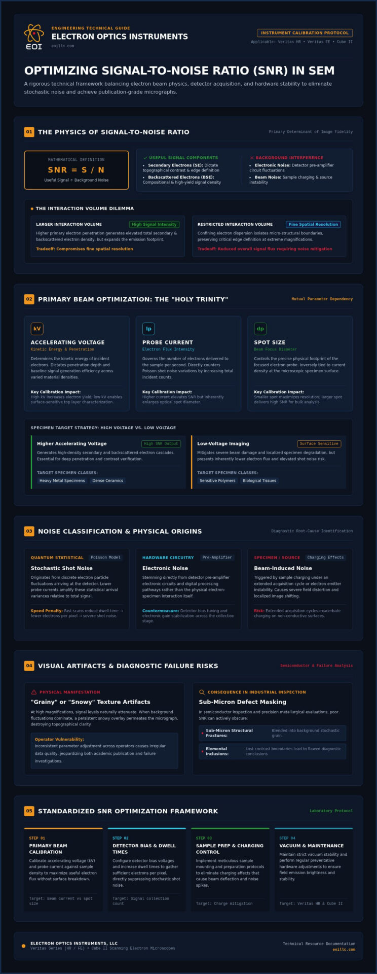
Improving SNR in SEM: A 5-Step Workflow
Achieving high-fidelity micrographs requires more than just high-end hardware; it demands a methodical operational cadence. While post-processing software offers some relief, the foundation of improving signal to noise ratio in sem lies in meticulous hardware calibration and environmental management. This five-step workflow provides a structured approach for laboratory professionals to eliminate grainy artifacts and ensure data integrity across all scanning cycles.
- Step 1: Begin with meticulous SEM sample preparation to ensure maximum conductivity. Non-conductive surfaces lead to localized charging, which creates massive noise spikes and topographical distortions.
- Step 2: Perform precise column alignment. Aperture centering ensures the electron path is stable and free from stray reflections that contribute to background interference.
- Step 3: Select the optimal accelerating voltage for your material density. Heavy metals allow for higher energy penetration, whereas polymers require lower voltage to prevent beam damage and maintain a clean signal.
- Step 4: Incrementally adjust the probe current while monitoring the live resolution. Increasing the current directly boosts the signal density, but it’s vital to stop before the spot size expands enough to blur fine structural details.
- Step 5: Apply frame averaging to finalize the high-resolution capture. This mathematical approach averages out random electronic fluctuations without the thermal risks or charging effects associated with a single, slow acquisition scan.
Preliminary Alignment and Stigmation
Poor stigmation often mimics image noise by creating subtle directional blurring that masks fine structural detail. Stigmation is the correction of beam asymmetry to ensure a circular focal point. Correcting this requires careful adjustment of the X and Y stigmators while observing the specimen at high magnification. Precise alignment of the final aperture is equally critical; an off-center aperture introduces aberrations that degrade the signal before it even reaches the specimen. If you’re utilizing advanced systems like the Veritas Series, these alignments must be verified daily to maintain consistent data quality.
Environmental and External Noise Control
External factors frequently introduce artifacts that operators mistake for internal instrument noise. Vibrational interference from nearby industrial machinery or electromagnetic fields from power lines can disrupt the electron path, leading to jagged edges in the micrograph. The integrity of the vacuum system is another pillar of stability. A degraded vacuum increases beam scattering, which raises the background noise floor and obscures compositional contrast. Ensuring your lab environment meets the rigorous specifications for advanced SEM techniques is a prerequisite for achieving sub-nanometer resolution. To ensure your instrument is operating at peak efficiency, you should schedule Preventative Maintenance Visits to verify your hardware’s baseline performance.
The Role of Instrument Maintenance in Maintaining High SNR
While beam physics and scan parameters provide the operational framework for high-resolution imaging, the physical integrity of the electron optical column remains the ultimate ceiling for performance. Hardware degradation often introduces subtle, compounding artifacts that no amount of software filtering can fully rectify. Meticulous attention to SEM maintenance is therefore the prerequisite for any laboratory focused on improving signal to noise ratio in sem. Contaminated apertures, in particular, act as a primary source of beam instability; carbon buildup from previous samples can cause erratic beam deflection and increased scattering, which raises the background noise floor and obscures fine topographical detail. Maintaining an established baseline of performance requires a visionary approach to hardware health that extends beyond the daily scan.
Filament Health and Source Brightness
A stable electron source is essential for a consistent probe. Whether your system utilizes a tungsten filament or a CeB6 cathode, end-of-life symptoms often manifest as a decrease in source brightness and an increase in beam current fluctuations. As the source weakens, operators often compensate by increasing the detector gain, which inadvertently amplifies electronic noise alongside the signal. Achieving source saturation is critical. A sub-optimal flux leads to the grainy textures that compromise industrial failure analysis. Utilizing high-quality SEM Filaments and Consumables ensures that the thermionic emission remains stable, allowing for the high-intensity signal required for ultra-high-resolution characterization without the penalty of increased electronic gain.
Professional Service and Preventive Maintenance
Vacuum integrity is another critical factor that dictates the baseline noise level of an instrument. Minor vacuum leaks introduce gas molecules into the column, leading to increased beam scattering and a reduction in signal collection efficiency. Regular Preventative Maintenance Visits are necessary to verify vacuum seals and ensure that the ion pumps are operating at peak capacity. For industrial labs, annual service contracts provide a reliable path toward repeatability, ensuring that systems like the Genesis Tabletop SEM or Veritas Plus perform at their original factory specifications. This professional oversight is the most effective strategy for improving signal to noise ratio in sem over the long term. On-site technical training further empowers your team to troubleshoot SNR issues at the hardware level before they impact your lab’s throughput or data accuracy.
Achieving Operational Excellence in Electron Optics
The pursuit of sub-nanometer resolution requires a rigorous commitment to technical meticulousness across every stage of the imaging process. As established, the foundation of clarity rests upon the synergy between primary beam optimization and the physical integrity of the electron optical column. By implementing standardized scanning protocols and prioritizing the health of critical hardware components, laboratories can successfully navigate the complexities of improving signal to noise ratio in sem. This methodical approach ensures that every micrograph meets the authoritative standards required for industrial failure analysis and academic publication.
Electron Optics Instruments, LLC brings over 30 years of industry experience to your facility, serving as the sole US distributor for the EmCraft Cube II and Genesis models. We provide national technical training and comprehensive service contracts designed to keep your Veritas Series or benchtop systems performing at peak factory specifications. Explore our Benchtop SEM solutions and professional service contracts at eoillc.com to stabilize your imaging environment and achieve the precision your research demands. With the correct integration of advanced hardware and expert-driven protocols, your lab is well-positioned to redefine the limits of what’s possible in modern microscopy.
Frequently Asked Questions
What is a good signal-to-noise ratio for SEM imaging?
A definitive signal-to-noise ratio is generally achieved when the useful signal is at least three to five times higher than the background noise floor. In high-resolution industrial failure analysis, a much higher ratio is required to distinguish sub-micron defects from stochastic fluctuations. Achieving this benchmark requires meticulous calibration of systems like the Veritas HR to ensure that topographical details remain distinct and authoritative across all magnification levels.
Does increasing the accelerating voltage always improve SNR?
Increasing accelerating voltage typically enhances signal yield due to deeper electron penetration and higher secondary electron generation, but it isn’t a universal solution. While it improves raw signal density, high voltage levels can induce beam damage in sensitive polymers or cause excessive charging in non-conductive specimens. Operators must balance voltage with material density to maintain structural integrity while improving signal to noise ratio in sem for reliable data acquisition.
How does working distance affect the signal-to-noise ratio?
Reducing the working distance generally improves the signal-to-noise ratio by increasing the solid angle of electron collection at the detector. A shorter distance between the specimen and the final lens allows the Everhart-Thornley detector to capture a higher percentage of secondary electrons. However, this adjustment limits the depth of field. Precise geometric positioning is essential for systems like the Genesis Tabletop SEM to maximize collection efficiency without risking hardware collisions.
What is the difference between image integration and frame averaging?
Image integration involves a single slow scan where the signal is accumulated over a prolonged dwell time, whereas frame averaging captures multiple rapid scans and mathematically combines them. Frame averaging is often preferred for non-conductive samples as it mitigates the localized charging effects associated with slow-speed scanning. Both techniques are vital for improving signal to noise ratio in sem, providing the stability required for publication-quality micrographs in demanding research environments.
Can software filters fix a low SNR image effectively?
Software filters can reduce the visual appearance of graininess, but they can’t replace the data lost to a poor initial signal. Post-processing algorithms often introduce blurring or artifacts that mask fine structural details essential for rigorous analysis. Relying on software is a secondary measure; primary focus should always remain on hardware optimization and meticulous column alignment to capture high-fidelity raw data from the outset of the scanning process.
Why does my SEM image look grainier at higher magnifications?
Graininess at high magnification occurs because the electron beam scans a smaller area, which naturally reduces the number of electrons interacting with the specimen per pixel. This reduction in signal density makes the underlying shot noise more prominent relative to the useful data. To counteract this, operators must increase the probe current or extend the acquisition time, ensuring that the signal remains robust enough to define sub-nanometer features clearly.
How often should I clean my SEM apertures to maintain signal quality?
Cleaning or replacing apertures should occur during every scheduled Preventative Maintenance Visit or whenever beam instability is observed. Contaminated apertures accumulate carbon deposits that cause erratic beam deflection and increased background scattering, directly degrading the signal quality. In high-throughput industrial settings, a quarterly inspection of the electron optical column is recommended to ensure that instruments like the Cube II maintain their peak resolution and operational reliability.
Does sample charging affect the signal-to-noise ratio?
Sample charging significantly degrades the signal-to-noise ratio by creating unstable electrostatic fields that deflect the primary beam and distort secondary electron emission. This phenomenon manifests as bright streaks or topographical shifts that obscure the true surface morphology. Meticulous sample preparation, including the application of conductive coatings, is essential to stabilize the specimen interface and ensure that the detected signal reflects actual structural data rather than charging artifacts.