

The assumption that modern automated software can independently resolve complex spectral interferences is a precarious foundation for high-precision materials characterization. While recent hardware advancements, such as the Bruker XFlash 7 series, now achieve throughput rates of up to 1,000,000 counts per second, the fundamental challenges in eds elemental mapping remain rooted in the intricate physical interactions between the electron beam and the specimen. Relying solely on default algorithms often leads to the misidentification of trace elements or the presence of phantom signals where none exist.
You likely recognize that even with sophisticated tools like the Oxford Instruments AZtec Suite 6.3, the presence of significant peak overlaps or geometric shadowing can quickly compromise the integrity of your elemental distribution data. It’s a persistent concern when extended acquisition times intended to improve signal-to-noise ratios instead result in irreversible beam damage to sensitive samples. This article provides the technical framework necessary to master these complexities, ensuring that your chemical characterization remains both accurate and free from common mapping artifacts. We’ll examine the strategic integration of hardware stability and sophisticated spectral deconvolution, alongside the practical application of new standards like ASTM E3501-25, to achieve the crisp, high-contrast results required in the current industrial landscape.
Key Takeaways
- Understand how Silicon Drift Detector (SDD) technology enables high-speed acquisition while maintaining the precision required for spatially resolved chemical analysis.
- Identify and mitigate geometric shadowing and suboptimal take-off angles that frequently impede accurate X-ray signal collection on complex topographical samples.
- Implement rigorous hardware stability protocols to overcome core challenges in eds elemental mapping, such as beam drift and environmental vibration during long-duration acquisitions.
- Distinguish between genuine elemental distributions and electronic artifacts, including sum peaks and the notorious Lead-Sulfur spectral overlap.
- Optimize your analytical workflow by leveraging the inherent stability of the Cube II Benchtop SEM to ensure reliable, high-contrast characterization of sensitive materials.
Understanding the Mechanism and Accuracy of EDS Elemental Mapping
Energy dispersive spectroscopy mapping represents a sophisticated fusion of high-resolution imaging and rigorous chemical quantification. It’s a spatially resolved technique that correlates X-ray emission data with specific pixel coordinates across a defined region of interest. This process relies on the fundamental principles of Energy-dispersive X-ray spectroscopy to identify elements based on their characteristic energy signatures. As we move through 2026, the demand for precision in microstructural analysis has moved beyond simple visualization. Modern Silicon Drift Detectors (SDDs) have revolutionized this field by providing high-speed acquisition rates without sacrificing the energy resolution required to distinguish between adjacent peaks in the periodic table. These detectors allow for the collection of millions of counts in minutes, a feat that was once a multi-hour endeavor.
Traditional “dot maps” merely record raw counts within a specific energy window, which often leads to misleading results due to background noise or overlapping signals. In contrast, quantitative net intensity mapping utilizes advanced algorithms to perform spectral deconvolution at every pixel. This distinction is vital when addressing the challenges in eds elemental mapping, particularly when analyzing complex multi-component alloys where minor peaks can be obscured by the bremsstrahlung background. The rigorous industry standards of 2026 demand this level of meticulousness to ensure that data reflects actual material composition rather than electronic artifacts. Reliable characterization now requires a synergy between hardware stability and sophisticated software capable of real-time background subtraction.
The Role of X-ray Generation Volume
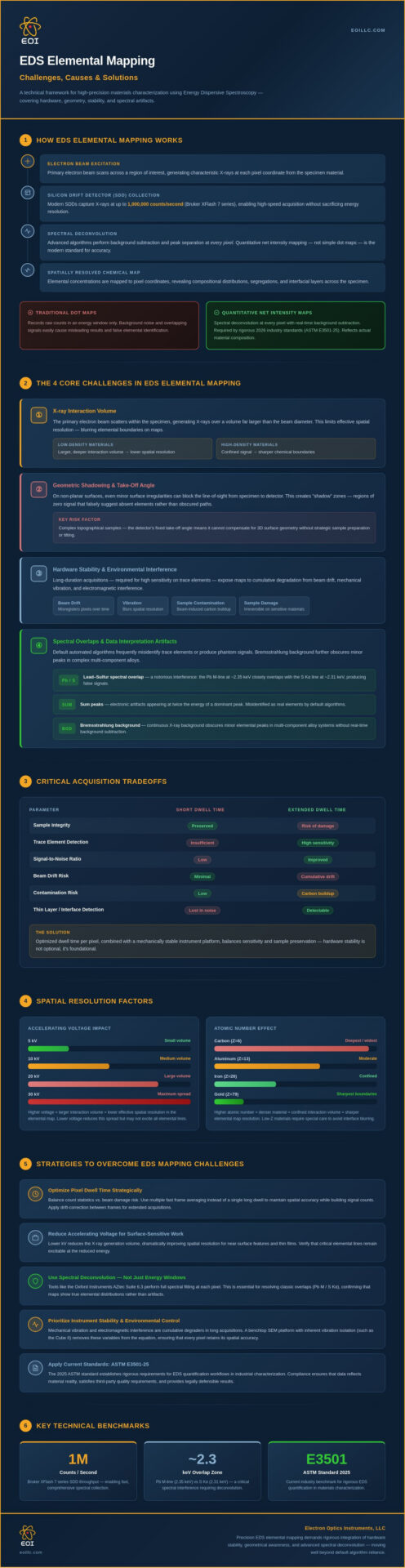
The interaction volume is the specific region within the specimen where the primary electron beam scatters and generates characteristic X-rays, and its dimensions are fundamentally determined by the accelerating voltage and the sample’s average atomic number. While a fine electron probe suggests high resolution, the lateral spread of X-rays often exceeds the beam diameter by several orders of magnitude. This phenomenon limits the effective spatial resolution of an elemental map. In low-density materials, the signal originates from a larger, deeper volume, whereas high-density specimens confine the signal, allowing for sharper chemical boundaries. Managing this volume is a critical step in ensuring that maps don’t suffer from blurred interfaces.
Spatial Resolution vs. Analytical Sensitivity
Achieving the ideal map requires a delicate balance between pixel dwell time and the total duration of the scan. Short dwell times might preserve sample integrity but often fail to provide enough counts for the reliable quantification of trace elements. Conversely, extended scans increase analytical sensitivity at the risk of beam-induced contamination or sample drift. Utilizing advanced SEM techniques allows operators to optimize these parameters, ensuring that high-resolution imagery doesn’t come at the cost of chemical accuracy. This synergy is essential for identifying localized segregations or thin interfacial layers that would otherwise be lost in the noise of a rapid, low-sensitivity scan.
Physical and Geometrical Challenges in X-ray Signal Acquisition
The physical geometry of the specimen-detector interface often presents the most significant hurdles in achieving accurate chemical characterization. Even with modern high-speed detectors, the line-of-sight requirement for X-ray collection remains absolute, creating inherent challenges in eds elemental mapping when analyzing non-planar surfaces. If the detector is positioned at a specific take-off angle, even minor surface irregularities can cast “shadows,” resulting in regions of zero signal that don’t reflect actual material composition but rather the absence of a clear path to the sensor. This geometric obstruction is particularly problematic in fractured specimens or additive manufacturing components where complex topographies are the norm rather than the exception.
Low-energy X-ray lines, such as those for Nitrogen and Oxygen, are particularly vulnerable to these geometric constraints because their escape depth is significantly shallower than higher-energy emissions. At low accelerating voltages, these limitations of EDS become a primary concern, as the matrix itself can absorb these signals before they ever exit the sample surface. This absorption isn’t uniform; it varies based on the local atomic number and the path length of the X-ray through the material. Achieving the precision required to overcome these artifacts necessitates a combination of meticulous sample preparation and robust hardware, such as the Cube II Benchtop SEM, which provides the stability needed for high-resolution analytical tasks.
Topographic Effects and Shadowing
Identifying “dark zones” in a map is a critical skill for any microscopist. These regions appear depleted of specific elements not due to chemical heterogeneity, but because the local surface tilt prevents X-rays from reaching the detector. Shadows mask truth. To mitigate these artifacts, practitioners often employ sample rotation or multi-detector systems to fill in missing data. However, flat, polished samples remain the gold standard for quantitative mapping, as they ensure a constant take-off angle across the entire field of view, eliminating the variables of local absorption and shadowing that otherwise skew net intensity calculations.
Matrix Effects: ZAF Corrections in Mapping
Quantitative accuracy in mapping relies on the ZAF correction model, which accounts for Atomic Number (Z), Absorption (A), and Fluorescence (F) effects within the sample matrix. These interactions can lead to the misinterpretation of elemental boundaries, especially at the interface of two distinct phases. Fluorescence occurs when a primary X-ray from a heavy element excites a secondary X-ray in a neighboring phase, effectively creating “ghost” signals that suggest the presence of an element in a region where it’s physically absent. Without rigorous spectral processing, these matrix effects can lead to overestimating the diffusion of elements across grain boundaries or phase transitions.
Hardware Stability and Environmental Interference
Precision in microanalysis is fundamentally dependent on the mechanical and electronic stability of the scanning electron microscope. While the previous sections explored physical geometry and detector mechanisms, the external environment and internal column health present a different set of challenges in eds elemental mapping. Even the most advanced Silicon Drift Detector can’t compensate for a primary electron beam that wanders during a ten-minute acquisition. Beam drift, often a result of thermal fluctuations within the column or electromagnetic interference, causes a spatial mismatch between the intended pixel coordinate and the actual X-ray generation site. This misalignment leads to blurred elemental boundaries and inaccurate phase identification, undermining the meticulousness required for rigorous industrial characterization.
Environmental factors, particularly low-frequency vibrations and acoustic noise, can introduce periodic artifacts that manifest as jagged edges in high-magnification maps. Maintaining a high-quality vacuum is equally critical. Poor vacuum levels increase the probability of carbon contamination, which attenuates low-energy X-rays and introduces phantom signals in light-element mapping. Ensuring the long-term reliability of these analytical results necessitates regular SEM maintenance. Meticulous calibration and preventative care of the electron optics and vacuum systems are the only ways to guarantee that the hardware performs to its theoretical specifications over years of high-stakes industrial operation.
The Impact of Beam Stability
Field emission sources provide inherently superior stability and brightness compared to thermionic sources, making them the preferred choice for long-duration mapping. Managing beam current fluctuations is essential. If the probe current varies during the scan, the resulting X-ray counts per pixel will fluctuate independently of the sample’s chemistry, distorting the final quantification. Thermal drift in the SEM column, often exacerbated by inconsistent laboratory temperatures, can shift the scan area by several nanometers. This shift effectively decouples the chemical data from the morphological image, a failure that no amount of post-processing can truly rectify.
Detector Dead Time and Pulse Processing
Optimizing the relationship between the input count rate and detector dead time is a balancing act that defines the throughput of an EDS system. When the detector is overwhelmed by an excessive count rate, it becomes “dead” to new incoming X-rays while processing previous pulses, leading to significant data loss and spectral distortion. This phenomenon can artificially suppress the signal from minor elements. To maximize signal capture without saturating the sensor, operators must optimize the solid angle by adjusting the detector’s proximity to the sample. This ensures the pulse processor can accurately resolve each individual X-ray event without introducing electronic noise or compromising the integrity of the spectral data.
Overcoming Spectral Overlaps and Data Interpretation Artifacts
The reliability of chemical mapping is often jeopardized not by hardware failure, but by the inherent physics of X-ray emission. One of the most pervasive challenges in eds elemental mapping is the presence of spectral overlaps, where characteristic X-rays from different elements occur at nearly identical energy levels. The classic conflict between the Lead (Pb) M-line and the Sulfur (S) K-line serves as a primary example; without sophisticated peak deconvolution, these two distinct elements are indistinguishable in a standard spectrum. Modern EDS systems must employ advanced mathematical models to strip these overlapping signals apart, ensuring that a map of a lead-acid battery or a sulfide ore reflects the true distribution of each species rather than a blurred composite of both.
Beyond physical overlaps, electronic artifacts like sum peaks and escape peaks introduce “phantom” elements into the data, potentially leading to costly misinterpretations. A Silicon escape peak occurs when an incoming X-ray excites a Silicon K-alpha photon within the detector crystal, which then escapes the sensor volume, leaving behind a signal at an energy level exactly 1.74 keV lower than the original line. Similarly, the Bremsstrahlung background radiation, a continuous X-ray spectrum caused by the deceleration of electrons within the sample, creates a “noise floor” that complicates the mapping of trace elements. This background radiation reduces the peak-to-background ratio, making it difficult to discern subtle chemical variations from stochastic noise, especially when dealing with elements present at concentrations below one weight percent.
Deconvolution vs. Window-Based Mapping
Traditional window-based mapping, which simply integrates counts within a fixed energy range, is increasingly viewed as insufficient for high-stakes industrial analysis in 2026. This method fails to account for background contributions or neighboring peak tails, often leading to false positives in automated element identification software. Net-intensity mapping, powered by full spectral imaging, allows for the subtraction of the Bremsstrahlung continuum and the deconvolution of overlapping peaks at every individual pixel. This rigorous approach is essential for identifying localized segregations in complex superalloys where minor constituents might otherwise be masked by the dominant matrix peaks. Relying on basic automated outputs without these corrections can compromise the entire narrative of a failure analysis or material characterization report.
Artifact Identification Checklist
To maintain analytical integrity, microscopists must systematically verify their mapping results against the original point spectra collected from the same region. A sum peak is an electronic artifact that occurs when two X-ray photons arrive at the detector at nearly the same instant, causing the pulse processor to record them as a single event with an energy value equal to the sum of the two individual photons. These artifacts are most prevalent during high-count-rate acquisitions where detector dead time is elevated. Distinguishing these from real elements requires a thorough understanding of the sample’s expected chemistry and the detector’s physical response. If you’re looking to upgrade your analytical capabilities and minimize these errors, exploring high-performance EDS Systems can provide the spectral resolution necessary to navigate these complexities with confidence.
Optimizing EDS Mapping with Cube II and Professional Support
Resolving the multifaceted challenges in eds elemental mapping necessitates a decisive shift from identifying theoretical hurdles to implementing robust, integrated solutions. While understanding the physics of X-ray generation and spectral deconvolution is foundational, the practical realization of accurate data depends on the synergy between high-performance hardware and expert operator proficiency. The Cube II Benchtop SEM is engineered to bridge this gap, providing a stabilized platform that minimizes the mechanical and thermal instabilities that frequently compromise long-duration acquisitions. By integrating advanced EDS systems directly into the primary software environment, researchers can transition seamlessly from morphological imaging to chemical characterization, significantly reducing the likelihood of spatial registration errors and data fragmentation.
Technical mastery of the equipment remains as critical as the hardware itself. User-induced artifacts, such as improper background subtraction or incorrect peak identification, can be mitigated through professional SEM operation training. This specialized education empowers operators to recognize the subtle nuances of sum peaks and escape peaks detailed in previous sections, ensuring that every map reflects genuine material chemistry. Beyond operator skill, the long-term accuracy of any analytical system relies on rigorous preventative maintenance visits. EOI’s field service team ensures that every component, from the electron source to the detector crystal, meets original manufacturer specifications, preserving the energy resolution required for 2026 industrial standards.
Strategic Hardware Integration
The Cube II Benchtop SEM is specifically designed for high-throughput industrial environments where reliability and speed are paramount. Its architecture optimizes the detector-sample geometry to achieve a superior solid angle, which maximizes X-ray collection efficiency even at lower accelerating voltages. This geometric precision is essential for mitigating the shadowing effects and absorption artifacts that often plague topographical samples. This tailored hardware integration ensures that the system adapts to the sample’s unique physical properties, allowing for customized EDS configurations across diverse material classes, from sensitive polymers to complex metallurgical alloys.
Professional Calibration and Maintenance
Maintaining a competitive edge in specialized sectors requires a commitment to meticulousness and international capability. Organizations facing particularly complex failure analysis often benefit from requesting a technical consultation to refine their analytical workflows. These high-level engagements, supported by comprehensive service contracts, act as a safeguard for your capital investment. Regular calibration of the pulse processor and vacuum system ensures that the hardware performs at its peak, providing the stability needed to resolve trace elements and maintain the integrity of your microstructural narrative.
Advancing Analytical Standards through Integrated Precision
Mastering the intricacies of microanalysis requires more than just high-speed detectors; it demands a rigorous commitment to hardware stability and sophisticated spectral deconvolution. By systematically addressing the challenges in eds elemental mapping, such as geometric shadowing and electronic artifacts, industrial professionals can ensure that their chemical characterization remains both accurate and defensible. The transition from qualitative visualization to quantitative net-intensity mapping is no longer optional, as the complexity of modern alloys necessitates a higher degree of meticulousness in data interpretation.
As an authorized US distributor for EmCraft SEMs with over 30 years of electron optics expertise, EOI provides the technical foundation required for these high-stakes applications. Our comprehensive national service and preventative maintenance support guarantee that your instrumentation consistently operates at peak performance. We invite you to Explore our Cube II Benchtop SEM and Integrated EDS Solutions to see how optimized geometry and superior beam stability can transform your analytical outcomes. We look forward to supporting your progress toward unprecedented levels of microstructural clarity.
Frequently Asked Questions
What is the most common cause of noise in EDS elemental maps?
The primary cause of noise in elemental maps is a statistically insufficient X-ray count rate at each individual pixel coordinate. This phenomenon typically occurs when the dwell time is too short to accumulate enough signal relative to the stochastic fluctuations of the background Bremsstrahlung radiation. To resolve this, operators must increase the total acquisition duration or optimize the beam current, though they must remain vigilant regarding sample stability and potential beam damage.
How does accelerating voltage (kV) affect the quality of an EDS map?
Accelerating voltage dictates the dimensions of the interaction volume and the efficiency of X-ray excitation for specific elements. While higher voltages are necessary to excite high-energy K-lines, they simultaneously increase the lateral spread of the signal, which often degrades the spatial resolution of the map. Conversely, lower voltages improve surface sensitivity but can introduce significant challenges in eds elemental mapping by failing to provide sufficient overvoltage for heavier elements.
Can I perform EDS mapping on non-conductive samples without coating?
Performing EDS on non-conductive, uncoated samples is achievable through the utilization of low-vacuum SEM modes or by operating at the charge-neutral point at low accelerating voltages. These techniques effectively dissipate surface charge by using residual gas ions or by balancing electron emission. However, these methods often necessitate a compromise in spatial resolution and can increase the background noise due to gas-path scattering of the primary electron beam.
What is spectral deconvolution and why is it necessary for mapping?
Spectral deconvolution is a sophisticated mathematical process used to separate overlapping X-ray peaks that occupy the same energy range. It’s necessary because standard ROI mapping cannot distinguish between elements with nearly identical energy signatures, such as the classic Lead and Sulfur overlap. By applying deconvolution at every pixel, modern software ensures that the resulting map represents the true chemical distribution rather than an inaccurate composite of interfering signals.
How do I distinguish between a real elemental signal and a sum peak?
Distinguishing between a real signal and a sum peak involves verifying the energy position against the major peaks present in the spectrum. A sum peak is an electronic artifact found at an energy level equal to the sum of two high-intensity peaks, such as two Silicon K-alpha photons. It’s most prevalent at high count rates; therefore, reducing the beam current or increasing the detector distance should cause the artifact to diminish if it isn’t a real element.
What is the optimal dead time for high-accuracy EDS mapping?
For high-accuracy analytical mapping, an optimal detector dead time typically ranges between 20% and 40%. This specific range provides a balance between high throughput and the precision of the pulse-processing electronics. Operating beyond 50% dead time significantly increases the risk of data loss and spectral distortion, while maintaining a very low dead time often results in inefficiently long acquisition periods that can exacerbate beam drift issues.
Why does my EDS map look “shadowed” on one side of a particle?
Shadowing artifacts occur when the local topography of a sample physically obstructs the line-of-sight path between the X-ray generation site and the detector. Because X-rays travel in straight lines, any protrusion on the specimen surface can cast a chemical shadow where no signal is recorded. This is a fundamental geometric constraint that requires careful sample orientation or the use of multiple detectors to ensure uniform signal collection across complex surfaces.
How often should I calibrate my EDS detector for elemental mapping?
Calibrating the EDS detector should occur at regular intervals to maintain the integrity of the energy scale and resolution. While modern Silicon Drift Detectors are remarkably stable, performing a quick gain calibration with a known standard like Copper is recommended at the start of each analytical session. A more comprehensive calibration should be integrated into a monthly preventative maintenance schedule to address the persistent challenges in eds elemental mapping and ensure long-term data consistency.