

The fundamental limitations of optical physics have reached a critical threshold in contemporary manufacturing, where the inability to resolve sub-micron features represents a significant barrier to industrial progress. You likely recognize that traditional light microscopy fails to provide the depth of field required for complex topographical assessment, often leaving engineers unable to identify the precise elemental nature of microscopic contaminants. This analytical gap is especially pronounced when implementing sem for semiconductor analysis, as the industry’s 2026 transition toward High-NA EUV lithography and modular chiplet architectures necessitates unprecedented levels of structural verification.
This comprehensive guide details how advanced Scanning Electron Microscopy (SEM) drives innovation across material science, electronics, and the life sciences through superior high-resolution imaging. By reading further, you’ll gain a clear understanding of the distinction between topographical and compositional analysis, alongside a methodical framework for hardware selection. We will evaluate the specific utility of systems ranging from the rapid diagnostic capabilities of the Cube II benchtop SEM to the high-end research potential of the Veritas FE series, ensuring your laboratory infrastructure aligns with your specific operational requirements.
Key Takeaways
- Understand the technical advantages of Scanning Electron Microscopy over traditional optical systems, particularly regarding superior depth of field and the precision of elemental composition analysis.
- Explore the critical utility of sem for semiconductor analysis in navigating the complexities of defect inspection and sub-micron circuit visualization within modern electronic architectures.
- Examine the strategic application of SEM in material science for conducting grain boundary analysis and identifying the fundamental mechanisms behind mechanical failures.
- Identify the specific forensic and biological use cases for high-resolution imaging, ranging from trace evidence examination to the detailed characterization of cellular structures.
- Establish a rigorous framework for hardware procurement, balancing sample throughput requirements against the specialized resolution capabilities of benchtop and full-sized systems.
The Versatility of Scanning Electron Microscope (SEM) Applications
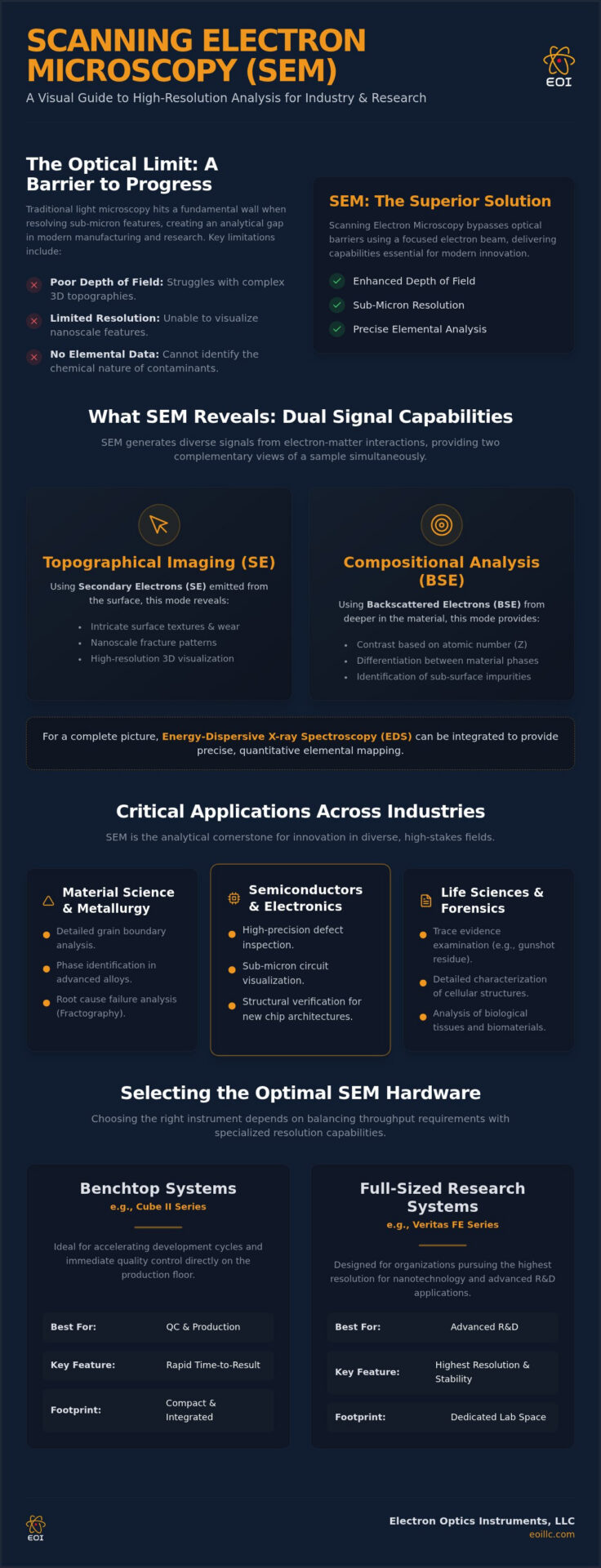
The fundamental constraints of visible light microscopy have historically limited the precision of microstructural characterization, necessitating a shift toward the superior capabilities of electron-based systems. A Scanning Electron Microscope (SEM) bypasses these optical barriers by utilizing a focused beam of accelerated electrons to achieve resolutions far beyond the sub-micron threshold. This transition provides a significantly enhanced depth of field, allowing for the clear visualization of complex three-dimensional topographies that traditional lenses cannot resolve. Modern SEM applications act as the critical bridge between raw analytical data and actionable industrial problem-solving.
The utility of these instruments arises from the interpretation of diverse signals generated by electron-matter interactions. Secondary Electrons (SE) are primarily emitted from the specimen surface, providing high-resolution topographical data that reveals intricate textures and fracture patterns. Conversely, Backscattered Electrons (BSE) originate from deeper within the material and offer contrast based on the atomic number of the elements present. This dual-signal capability is a cornerstone of modern material science, particularly when implementing sem for semiconductor analysis to identify surface-level defects and sub-surface impurities simultaneously.
Topographical Imaging vs. Elemental Analysis
SE imaging allows engineers to observe nanoscale surface wear and fracture modes with exceptional clarity, which is essential for conducting rigorous failure analysis on high-precision components. When paired with BSE detectors, the instrument can differentiate between materials based on chemical density, effectively mapping the distribution of different phases across a sample. For a comprehensive assessment, the integration of EDS Systems enables precise chemical mapping, transforming a visual image into a detailed elemental report. This synergy is vital for distinguishing between benign surface artifacts and critical material contaminants.
Why Industrial Labs Are Adopting SEM
The industrial landscape is moving away from reliance on centralized core facilities, choosing instead to integrate in-house hardware to accelerate development cycles. Benchtop units like the Cube II Benchtop SEM offer a compact footprint and rapid time-to-result, making them ideal for immediate quality control on the production floor. Organizations seeking higher resolution for nanotechnology applications often turn to the Veritas series, which provides the stability needed for advanced research. By consulting with Electron Optics Instruments, LLC, labs can effectively reduce logistical delays and gain a competitive edge in product reliability through meticulous technical integration and on-site training.
Material Science and Metallurgy: Characterizing the Microstructure
Precision in modern metallurgy requires more than surface-level observation; it demands a rigorous understanding of a material’s internal architecture. Scanning Electron Microscopy offers a definitive pathway to this understanding by enabling detailed grain boundary analysis and phase identification. These elements are critical when developing advanced alloys or high-performance composites intended for extreme environments. Quantitative analysis of inclusions and precipitates within metal matrices allows engineers to predict material behavior under mechanical stress with high accuracy. While metallurgy often focuses on bulk metals, these characterization principles are essential when utilizing sem for semiconductor analysis to inspect the structural integrity of lead frames and wide-bandgap materials like Silicon Carbide.
Failure Analysis and Fractography
Fractography remains a cornerstone of mechanical failure investigation in industrial laboratories. By utilizing high-resolution imaging, specialists can distinguish between fatigue, cleavage, and ductile fracture modes. Identifying these specific modes is the first step in determining the root cause of a component’s failure. Researchers often employ advanced SEM techniques to map stress points and analyze oxidation layers at the micro-level. This meticulous approach is equally vital in semiconductor failure analysis, where the chemical degradation of multi-layer interconnects can lead to system-wide instability. Detailed corrosion studies further reveal how oxidation and chemical exposure compromise the microstructural stability of critical hardware over time.
Powder Metallurgy and Additive Manufacturing
The global shift toward additive manufacturing has intensified the need for rigorous raw material characterization. Characterizing powder morphology and size distribution is now a prerequisite for successful 3D printing applications, as irregular particles can lead to inconsistent layer deposition. SEM imaging detects internal porosity and fusion defects in laser-sintered parts that optical systems simply cannot resolve. Ensuring the structural integrity of raw materials through SEM-based quality assurance prevents costly production errors and ensures that finished components meet international safety standards. This level of scrutiny is indispensable for organizations pushing the boundaries of 3D integration and advanced packaging.
Organizations looking to implement these rigorous protocols can explore how the Veritas Series provides the high-resolution research capabilities needed for advanced material characterization. Maintaining a competitive edge in manufacturing requires a partner that understands the synergy between industrial performance and meticulous technical integration. By adopting in-house SEM solutions, labs don’t just see their materials; they master the microstructural variables that define product success.
SEM for Semiconductor Analysis and Electronics Manufacturing
The semiconductor industry’s progression toward sub-5nm nodes and advanced 3D packaging requires analytical tools that surpass the physical limits of visible light. Scanning Electron Microscopy plays a critical role throughout the entire lifecycle, providing the precision necessary for high-resolution defect inspection and structural validation. By utilizing sem for semiconductor analysis, engineers can visualize sub-micron circuit paths and multi-layer interconnects with exceptional clarity, ensuring that complex architectures meet rigorous performance standards. This methodology is indispensable for non-destructive testing, as it allows for the examination of sensitive components without compromising their functional integrity during the diagnostic process.
The integration of benchtop systems, such as the Cube II, has revolutionized at-line inspection within cleanroom environments. These compact units provide rapid feedback loops, allowing technicians to identify processing errors immediately rather than waiting for results from a centralized laboratory. This shift toward decentralized microscopy minimizes production downtime and enhances overall yield by enabling real-time adjustments to fabrication parameters. Such agility is vital as the industry transitions toward High-NA EUV lithography and modular chiplet designs, where even minor misalignments can lead to significant yield loss.
Integrated Circuit (IC) Inspection
Integrated Circuit (IC) Inspection involves meticulous cross-sectional analysis of silicon wafers to verify layer thickness and alignment. This process is vital for identifying structural anomalies that stem from thermal cycling or mechanical stress. As noted in research regarding SEM in semiconductor device analysis, the ability to observe these devices at a micro-scale is fundamental to modern diagnostics. Key inspection protocols include:
- Identifying wire bond failures and solder joint fatigue in microelectronics.
- Detecting trace contaminants via EDS to prevent electrical shorts or leakage.
- Verifying multi-layer interconnect alignment in 3D IC stacking and advanced packaging.
Nano-Electronics and MEMS
The development of Micro-Electro-Mechanical Systems (MEMS) requires functional verification through high-magnification imaging to ensure moving parts operate as intended. Prototyping these sophisticated sensors relies heavily on high-performance benchtop microscopy to maintain rapid developmental cycles. Beyond traditional silicon, SEM is essential for characterizing carbon nanotubes and 2D materials that define the next generation of sensor technologies. Utilizing sem for semiconductor analysis at this level allows researchers to navigate the complexities of nanoscale engineering with absolute certainty, ensuring that emerging computing paradigms like neuromorphic computing are grounded in structural reality.
Life Sciences and Forensic Investigation: Exploring Biological Complexity
The application of Scanning Electron Microscopy extends far beyond the rigid structures of metallurgy and electronics, providing essential insights into the fluid complexity of biological systems. In the life sciences, SEM serves as a definitive tool for characterizing the morphology of cells, tissues, and microorganisms at resolutions that reveal the fundamental mechanics of life. While the sample preparation protocols for hydrated biological specimens are distinct from those used in sem for semiconductor analysis, the requirement for high-resolution structural verification remains a constant across both disciplines. This versatility allows researchers to bridge the gap between macroscopic observation and the nanoscale realities of pharmaceutical development and forensic investigation.
Biomedical and Pharmaceutical Research
In the biomedical sector, SEM imaging is indispensable for evaluating the topographical compatibility of dental implants and the success of bone-scaffold integration. These high-resolution assessments ensure that synthetic materials interface correctly with organic tissues, reducing the risk of clinical failure. Pharmaceutical laboratories utilize electron optics for the rigorous quality control of pill coatings and the performance of time-release drug capsules. By characterizing virus-like particles and bacterial biofilms, clinical researchers gain the data necessary to develop more effective therapeutic interventions. The meticulous nature of this research demands hardware that offers both stability and precision.
Forensic Science and Trace Evidence
Forensic investigation relies on the analytical power of SEM to transform microscopic trace evidence into admissible legal data. Automated Gunshot Residue (GSR) detection, facilitated by integrated SEM-EDS workflows, allows high-throughput laboratories to process evidence with unprecedented speed and accuracy. This methodology is equally effective for the comparative analysis of paint chips and glass fragments recovered from investigative scenes. Criminalistics also utilizes SEM to analyze the distinct morphology of pollen, fibers, and hair, providing a level of detail that optical systems cannot achieve.
Document verification represents another critical forensic application. By analyzing ink layers and paper fibers, specialists can detect sophisticated forgeries that are invisible to the naked eye. The stability required for these forensic protocols is often found in advanced hardware systems designed for international capability. For organizations seeking to enhance their investigative or research throughput, you can explore our full range of Veritas and Cube II SEM systems to find the ideal balance of resolution and sample capacity. Whether you’re investigating a crime scene or conducting sem for semiconductor analysis, the right electron optics infrastructure is the foundation of reliable data.
Selecting the Optimal SEM Hardware for Your Application
Choosing the right hardware requires a strategic assessment of your laboratory’s throughput objectives and the specific resolution thresholds of your target materials. While previous sections explored the diverse applications of electron optics, the procurement decision hinges on balancing immediate diagnostic needs with long-term research goals. When configuring sem for semiconductor analysis, for instance, you must decide if the priority is rapid defect screening or the extreme resolution required for next-generation gate characterization. High-precision industries don’t just need images; they need reliable uptime, which is why a commitment to preventative maintenance is a critical factor in the final selection process.
Benchtop vs. Floor-Model SEM
The Cube II Benchtop SEM is engineered for environments where footprint and speed are the primary drivers of industrial performance. It’s particularly effective for failure analysis where samples are small and results are needed in minutes to keep production lines moving. However, as the complexity of your research increases, the Veritas Series provides the necessary stability and higher accelerating voltages for sub-nanometer imaging. The nuances of SEM operation also vary significantly between these platforms, with benchtop units offering streamlined workflows for non-specialist operators. It’s vital to weigh the initial investment against the potential for future-proofing your analytical capabilities as international standards evolve.
The Role of Integrated EDS and Training
Chemical characterization is a non-negotiable requirement for approximately 90% of industrial SEM applications. Without integrated EDS, a lab is often left with visual data that lacks the elemental context needed for definitive root-cause identification. Maximizing the utility of this sophisticated hardware requires more than just high-spec detectors; it demands professional on-site technical training to ensure your staff can navigate complex sample preparation and imaging protocols. By consulting with Electron Optics Instruments, LLC, you can align your hardware procurement with specific industrial standards. This expert-driven approach ensures that your chosen system doesn’t just meet current requirements but serves as a reliable anchor for your facility’s ongoing technological advancement and logistical excellence.
Advancing Industrial Precision through Electron Optics
The mastery of electron optics has fundamentally redefined the parameters of industrial quality and research accuracy. Throughout this guide, we’ve examined how the transition from traditional light-based systems to advanced electron microscopy addresses the inherent topography and composition challenges faced by modern laboratories. Whether implementing sem for semiconductor analysis to secure supply chain integrity or conducting high-resolution metallurgical assessments, the ability to visualize the invisible is no longer a luxury but a prerequisite for global competitiveness.
Navigating the complexities of hardware integration requires a seasoned partner committed to technical meticulousness. With more than 30 years of industry experience and our position as the sole US distributor for EmCraft, Electron Optics Instruments, LLC delivers the specialized expertise required to bridge the gap between procurement and performance. Our comprehensive service and preventative maintenance plans are designed to safeguard your investment and ensure long-term operational stability. We encourage you to Request a Consultation for Your Specific SEM Application to evaluate how our Veritas and Cube II systems can transform your analytical throughput. Elevating your facility’s standards begins with a rigorous commitment to microscopic precision.
Frequently Asked Questions
What are the most common industrial applications of SEM?
SEM is utilized extensively for structural verification and defect inspection across diverse sectors. In metallurgy, it facilitates grain boundary analysis and phase identification; in electronics, it’s essential for verifying circuit integrity. Forensics labs use it for gunshot residue detection, while pharmaceutical firms analyze drug delivery systems. The technology bridges the gap between macroscopic observation and nanoscale engineering, providing the data needed for rigorous industrial quality control.
Can SEM be used for elemental analysis as well as imaging?
Yes, SEM provides comprehensive chemical data when integrated with Energy Dispersive Spectroscopy (EDS) systems. While the electron beam generates topographical images, the resulting X-ray emissions allow for precise elemental mapping. This capability is vital for identifying the composition of microscopic contaminants or verifying alloy constituents. Modern labs rely on this synergy to transform visual evidence into a detailed chemical report, ensuring every structural anomaly is fully characterized.
How does SEM application differ from light microscopy?
Scanning Electron Microscopy surpasses light microscopy by utilizing accelerated electrons rather than photons to resolve features. This fundamental shift allows for significantly higher magnification and a superior depth of field. While optical systems are limited by the wavelength of visible light, SEM achieves sub-nanometer resolution. It’s the preferred choice for inspecting complex three-dimensional topographies that appear blurred or indistinct under traditional lenses in high-precision manufacturing environments.
Is SEM suitable for imaging biological samples?
SEM is highly effective for imaging biological samples, though it requires specific preparation to withstand the vacuum environment. Researchers use it to observe the intricate morphology of cells, tissues, and microorganisms with exceptional clarity. In the pharmaceutical sector, it’s used to characterize bacterial biofilms and virus-like particles. By utilizing specialized coating techniques, labs can visualize organic structures at resolutions that reveal the fundamental mechanics of biological interaction.
What is the role of SEM in failure analysis?
SEM is the primary tool for identifying the root cause of mechanical and electrical failures. Through fractography, engineers can distinguish between fatigue, cleavage, and ductile fracture modes. In electronics, implementing sem for semiconductor analysis allows for the visualization of sub-micron circuit failures or wire bond fatigue. This meticulous diagnostic approach ensures that organizations can implement corrective actions based on concrete microstructural evidence rather than speculative theories.
What industries benefit most from benchtop SEM applications?
Manufacturing and electronics sectors gain the most from benchtop systems due to their rapid time-to-result and compact footprint. The Cube II Benchtop SEM is particularly effective for at-line inspection, allowing technicians to identify production defects immediately. Aerospace and automotive industries also utilize these units for quick quality checks of high-precision components. These systems democratize high-resolution imaging, moving it from centralized core facilities directly onto the production floor.
How do I choose between a benchtop and a full-sized SEM for my application?
Your choice depends on the required resolution and the nature of your samples. Benchtop models like the Cube II are ideal for rapid industrial failure analysis where speed is a priority. For specialized research requiring sub-nanometer resolution, including sem for semiconductor analysis, the Veritas Series is the superior option. Evaluating sample throughput against the need for advanced field emission (FE) capabilities will define the most cost-effective hardware strategy.
What are the limitations of SEM applications for non-conductive samples?
Non-conductive samples can accumulate surface charge, which often leads to image distortion or charging artifacts. To mitigate this, labs typically apply a thin conductive coating of gold or carbon to the specimen. Alternatively, some systems offer low-vacuum modes that neutralize charge through ionized gas molecules. While these steps add to the preparation timeline, they’re necessary for achieving the high-resolution data required for accurate material characterization in industrial and research settings.