

Does the structural integrity of your sample truly withstand the invasive nature of mechanical preparation, or are you inadvertently documenting artifacts instead of authentic morphology? For many industry professionals, preparing cross-sections for sem analysis represents a persistent challenge where mechanical smearing and non-conductive charging frequently obscure the delicate interfaces of thin-film architectures. You’ve likely experienced the frustration of deformation in soft materials or the prohibitive costs associated with specialized equipment that fails to deliver repeatable results. This technical guide empowers you to master the rigorous methodologies and sophisticated workflows required to generate artifact-free cross-sections for high-resolution microscopy. We’ll explore the strategic intersection of mechanical polishing and ion-beam techniques, providing a detailed roadmap for achieving precise measurements of layer thicknesses. By adopting these expert-driven standards, you’ll enhance the analytical capabilities of advanced systems like the Veritas Series or Cube II, ensuring your quality control processes remain both consistent and authoritative.
Key Takeaways
- Identify the critical distinctions between epoxy and conductive resins to ensure structural stability and minimize charging during the encapsulation process.
- Master the technical workflows of Argon Ion Milling and site-specific FIB lift-out to achieve the nanometer-scale precision required for modern thin-film characterization.
- Implement specialized cryogenic and sputter-coating protocols for preparing cross-sections for sem analysis when handling soft polymers or highly insulating materials.
- Optimize benchtop SEM parameters, including accelerating voltage and spot size, to leverage the full high-resolution capabilities of systems such as the Cube II and Veritas Series.
The Strategic Importance of Preparing Cross-Sections for SEM Analysis
The fundamental objective of preparing cross-sections for sem analysis is to expose the internal morphology and subsurface interfaces of a specimen with absolute fidelity. While surface topography provides critical data regarding external features, it’s often insufficient for evaluating the structural integrity of layered materials, complex coatings, or semiconductor packaging. In these high-stakes industrial applications, the critical performance metrics reside within the internal architecture. High-performance systems like the Veritas Series or the Cube II Benchtop SEM possess the resolution to resolve nanometer-scale features, yet the utility of this hardware is entirely dependent on the quality of the prepared interface. As we look toward 2026 standards, advancements in benchtop electron optics mean that sample preparation, rather than the microscope’s resolving power, has become the primary determinant of analytical success.
Core Objectives in Subsurface Characterization
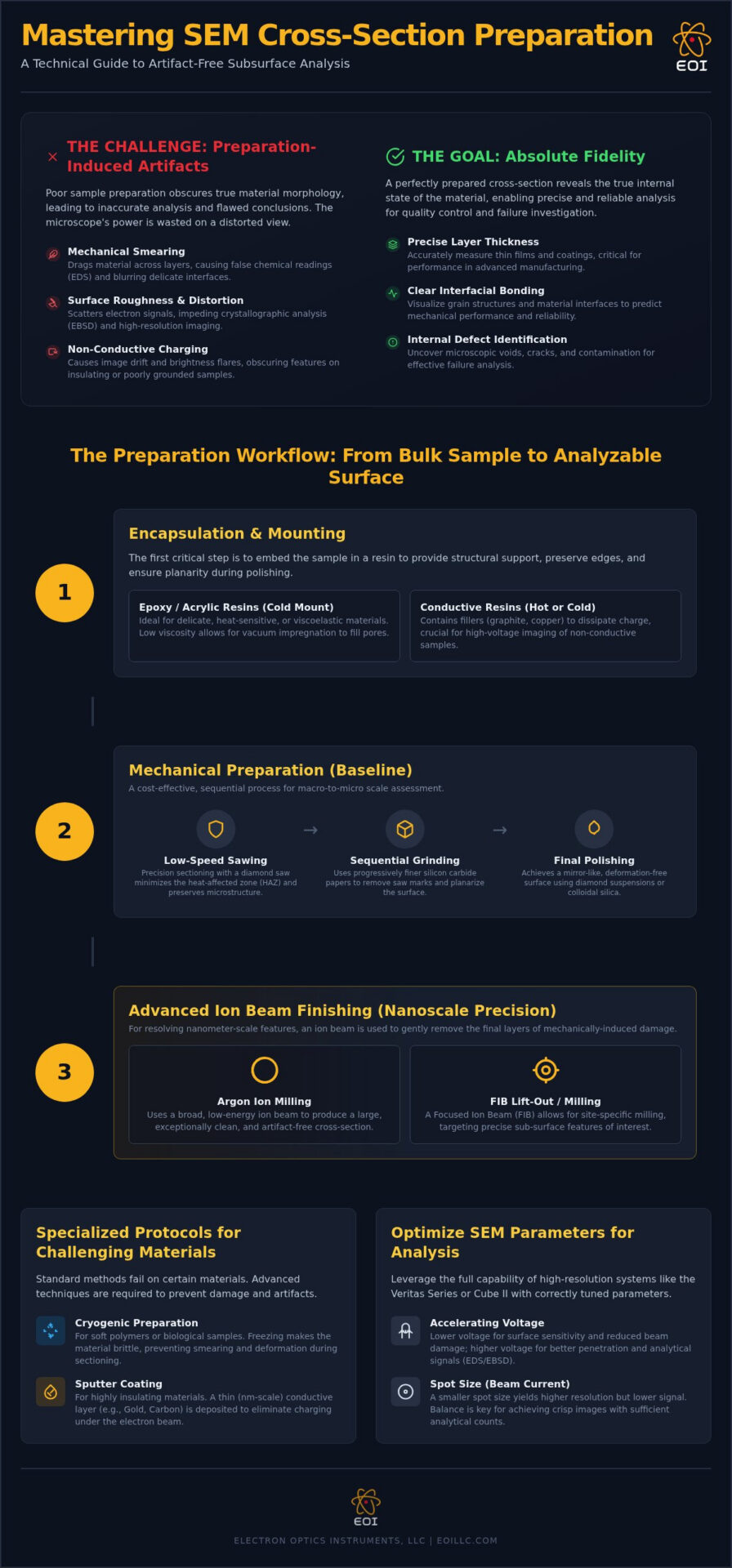
Subsurface characterization serves several strategic functions in a professional laboratory setting. Engineers must visualize grain structures and interfacial bonding to predict mechanical performance under stress. Precise measurements of thin film and coating thickness are mandatory for quality control in advanced manufacturing, where even a few nanometers of variance can lead to component failure. Without a clean cross-section, identifying internal defects such as microscopic voids, cracks, or localized contamination during failure analysis becomes impossible. These insights allow for the iterative refinement of production processes, ensuring that the final hardware meets rigorous international standards for reliability and performance.
Preparation Quality vs. Analytical Integrity
Analytical integrity is inextricably linked to the meticulousness of the preparation workflow. Mechanical smearing, a common artifact in poorly executed cuts, can drag material from one layer to another. This leads to false Energy Dispersive Spectroscopy (EDS) readings that misrepresent the sample’s chemistry. Similarly, surface roughness and lattice distortion significantly impede Electron Backscatter Diffraction (EBSD) by scattering the signal and obscuring crystallographic information. Achieving a surface that truly represents the bulk material requires a transition from rudimentary cutting to sophisticated, repeatable methodologies. Mastering these techniques ensures that the data gathered reflects the specimen’s actual state rather than preparation-induced changes, providing a stable foundation for technical innovation and logistical excellence.
Mechanical Preparation: Sawing, Grinding, and Polishing
Mechanical preparation remains the analytical baseline for most industrial laboratories, providing a cost-effective and versatile pathway to subsurface visualization. While ion-beam techniques offer superior precision at the nanoscale, the disciplined execution of sawing, grinding, and polishing is essential for macro-to-micro scale assessments. Successfully preparing cross-sections for sem analysis through mechanical means requires a rigorous adherence to sequential workflows to avoid the common pitfalls of smearing and edge rounding. This process transforms a bulk specimen into a planar interface capable of reflecting the material’s true internal state without the introduction of excessive mechanical artifacts.
Encapsulation and Mounting Techniques
The selection of a mounting medium is the first critical decision in the preparation sequence. Cold mounting, typically utilizing low-viscosity epoxies or acrylics, is the preferred route for specimens with low melting points or delicate viscoelastic properties. In contrast, hot compression mounting provides a superior bond and higher mount hardness, which is instrumental in maintaining planarity across multi-layered samples. For porous architectures or complex composites, vacuum impregnation is mandatory. This technique forces resin into internal voids, preventing the entrapment of air that would otherwise lead to catastrophic outgassing within the vacuum chamber of a Veritas Pro SEM. Incorporating conductive fillers like graphite or copper into the resin can also assist in dissipating charge during high-voltage imaging.
Precision Sectioning and Grinding
Sectioning must be performed with minimal kinetic energy to preserve the specimen’s native microstructure. Low-speed diamond sawing is the standard for minimizing the heat-affected zone (HAZ), as excessive frictional heat can induce phase changes or recrystallization in metallic samples. Once sectioned, the specimen undergoes sequential grinding using silicon carbide papers of increasing fineness. Practitioners must clean the sample thoroughly between every grit transition; a single stray particle from a 320-grit stage can compromise the results of a 1200-grit finish. This meticulousness ensures that the final surface is prepared for high-resolution characterization.
Final polishing stages utilize diamond suspensions or colloidal silica to achieve a deformation-free surface. Achieving this level of technical proficiency is often best supported through the specialized on-site technical training provided by Electron Optics Instruments, LLC, which bridges the gap between theoretical knowledge and practical laboratory excellence. By mastering these foundational steps, researchers ensure their data remains an accurate representation of the bulk material, providing the stability required for long-term industrial innovation.
Advanced Cross-Sectioning: Ion Milling and FIB
While mechanical polishing serves as a robust foundational technique, the pursuit of nanometer-scale fidelity often necessitates advanced ion-based methodologies. Argon Ion Milling, or Broad Ion Beam (BIB) processing, utilizes an inert gas stream to abrade the specimen surface at a molecular level, effectively removing the amorphous damage layer left by mechanical grinding. In contrast, Focused Ion Beam (FIB) lift-out procedures provide unparalleled site-specific preparation, allowing researchers to isolate features of interest with microscopic precision. When preparing cross-sections for sem analysis, the choice between BIB and FIB hinges on the required throughput; BIB is ideal for large-area surveys, whereas FIB is reserved for targeted, high-resolution diagnostics within systems like the Veritas Ultra or Veritas FE SEM.
Broad Ion Beam (BIB) Polishing Workflow
The BIB polishing workflow relies heavily on precise masking techniques to shield the sample surface, ensuring that only the cross-sectional face is exposed to the ion stream. Operators must optimize beam voltage and incident angles based on material density to prevent curtaining or differential milling rates. Post-milling inspection is vital to confirm that all preparation-induced deformation has been eliminated, leaving a pristine interface for high-contrast imaging. Thermal management remains a critical variable during this process, as prolonged ion bombardment can generate localized heat sufficient to melt or alter the structural morphology of sensitive specimens.
Mechanical vs. Ion Beam Preparation
The decision to implement ion beam preparation involves a strategic cost-benefit analysis. While the initial investment in ion milling hardware is higher than traditional mechanical equipment, the resulting analytical accuracy often justifies the expenditure for high-consequence failure analysis. Material suitability also plays a decisive role; for instance, ceramics and hard metals respond excellently to ion beams, while certain polymers may suffer from chain scission or thermal degradation if parameters aren’t strictly controlled. The perfect cross-section is one where the lattice structure remains undisturbed by preparation forces. By integrating these advanced workflows, laboratories ensure that their Veritas Series instruments operate at peak performance, delivering data that is both repeatable and scientifically sound.
Specialized Prep for Challenging Material Classes
Heterogeneous specimens, such as metal-ceramic joints, present a unique set of preparation challenges due to the stark contrast in material hardness. When preparing cross-sections for sem analysis, the differential removal rates during grinding can lead to relief formation or significant gaps at the interface. Resin shrinkage remains a persistent technical hurdle. As the mounting medium cures, it may pull away from the specimen, creating a void that traps contaminants and polishing lubricants. Utilizing low-shrinkage epoxies and ensuring a meticulous vacuum-impregnation cleaning regimen are the first steps toward mitigating these interfacial artifacts and ensuring a stable platform for high-resolution imaging.
Conductive Prep for Insulating Materials
Insulating specimens require a robust discharge path to prevent the accumulation of surface charge. This accumulation often manifests as image distortion or brightness fluctuations that compromise analytical integrity. Carbon tape and silver paint serve as primary bridges between the sample and the mount. For high-resolution imaging, sputter coating cross-sections with iridium, gold, or carbon is often necessary. Carbon is preferred for EDS due to its low X-ray interference, while iridium provides the finest grain size for ultra-high resolution work. While Low-vacuum SEM (LV-SEM) modes on the Veritas Series can alleviate some charging, a properly prepared conductive coating remains the gold standard for high-contrast subsurface analysis.
Soft and Ductile Material Challenges
Soft metals like copper and high-purity aluminum are notoriously prone to mechanical smearing. In these cases, the material is literally dragged across the cross-section, obscuring grain boundaries and invalidating EDS data. Selecting specific non-aqueous lubricants and implementing chemical-mechanical polishing (CMP) can resolve these issues. CMP combines abrasive action with chemical etching to reveal the true microstructure without preparation-induced strain. For elastomers and soft polymers, cryogenic cross-sectioning is indispensable. By cooling the sample below its glass transition temperature, you can achieve a brittle fracture or a clean cut that avoids the plucking or pitting common at room temperature.
These specialized techniques require more than just the right hardware; they demand a deep understanding of material science and technical meticulousness. You can enhance your laboratory’s capabilities by investing in high-quality SEM filaments and consumables or scheduling a technical consultation to refine your specific preparation workflows for high-consequence failure analysis.
Optimizing the Workflow for Benchtop SEM Analysis
The transition from traditional floor-model systems to high-performance benchtop hardware requires a strategic recalibration of preparation standards. While the Cube II Benchtop SEM offers significant versatility in handling diverse cross-section mounts, the analytical output is fundamentally limited by the specimen’s initial state. Preparing cross-sections for sem analysis for these compact systems demands a focus on minimizing the interaction volume. By adjusting the accelerating voltage to lower levels, typically between 5kV and 10kV, operators can enhance surface sensitivity and resolve thin-film interfaces that would otherwise be penetrated by higher energy beams. Smaller spot sizes further refine this resolution, provided the cross-section is sufficiently planar and free of mechanical deformation.
Maximizing Image Quality on Tabletop Systems
Optimizing the working distance is essential for capturing the complex topography of a prepared cross-section. For layered materials, utilizing backscattered electron (BSE) imaging is particularly effective; it highlights Z-contrast between materials of different atomic numbers, allowing for the immediate identification of metallic inclusions within a polymer matrix or ceramic grains in a bond line. The Genesis Tabletop SEM serves as an ideal platform for these rapid quality control checks, providing the necessary throughput for industrial production lines without sacrificing the meticulousness required for failure analysis. Integrating Energy Dispersive Spectroscopy (EDS) with these prepared surfaces allows for comprehensive elemental mapping, transforming a simple image into a detailed chemical profile of the internal architecture.
Training and Long-Term Maintenance
Inadequate sample preparation is the most frequent cause of perceived poor SEM performance, often leading to unnecessary troubleshooting of the hardware itself. Beyond image quality, poorly prepared samples can actively damage the instrument. Resins that haven’t reached full cure or those with trapped volatiles will outgas in the vacuum chamber, contaminating the column and reducing the lifespan of your filaments. Protecting your investment requires a dual approach: rigorous preventative maintenance to ensure vacuum integrity and professional technical training to master advanced preparation techniques. Customized training sessions allow your team to develop repeatable workflows tailored to your specific industrial cross-sectioning needs, ensuring that your Veritas Series or Cube II systems remain reliable anchors of your analytical capability.
Advancing Analytical Precision Through Meticulous Preparation
Achieving nanometer-scale clarity in subsurface characterization requires a disciplined integration of advanced hardware and rigorous sample prep. As industrial standards evolve, the mastery of preparing cross-sections for sem analysis is the definitive factor in extracting high-fidelity data from complex thin-film architectures and multi-phase alloys. Whether you utilize traditional mechanical polishing or sophisticated ion-beam milling, the objective remains an undisturbed lattice structure that reflects the true internal morphology of your specimen.
Electron Optics Instruments, LLC brings over 30 years of industry experience to your laboratory, serving as the sole US distributor for EmCraft benchtop systems. We provide comprehensive on-site technical training and service to ensure your workflows remain artifact-free and repeatable. By prioritizing these meticulous standards, you ensure the long-term reliability of your analytical systems and the accuracy of your failure analysis protocols. We invite you to Request a Quote for Benchtop SEM Solutions and elevate your facility’s technical capabilities. You’re building a foundation for structural innovation through preparation excellence.
Frequently Asked Questions
What is the most common mistake when preparing cross-sections for SEM?
The most frequent error when preparing cross-sections for sem analysis is the application of excessive pressure during the mechanical grinding phase. This induces smearing, which drags material across layer boundaries and invalidates EDS data. Professionals must use a sequential approach with decreasing grit sizes and minimal load. This ensures the native microstructure remains visible without preparation-induced artifacts that obscure critical interface details in systems like the Veritas Series.
How do I prevent my resin from shrinking away from the sample during curing?
Mitigating resin shrinkage requires the selection of high-quality, low-shrinkage epoxy resins specifically formulated for metallographic mounting. You should avoid rapid, high-heat curing cycles that accelerate volumetric contraction. Instead, utilize a slow, room-temperature cure or a controlled vacuum impregnation process. This stabilizes the interface between the specimen and the mount, preventing the formation of gaps that trap lubricants and lead to problematic outgassing during high-vacuum imaging.
Can I use a standard diamond saw for all SEM cross-sectioning?
A standard diamond saw isn’t universal; you must match the cutting speed and blade type to the material’s hardness and thermal sensitivity. Low-speed diamond saws are essential for delicate electronic components to minimize the heat-affected zone. Conversely, high-speed saws are more efficient for bulk ceramic or metallurgical samples. Using the wrong tool can introduce subsurface cracks or recrystallization, which compromises the integrity of the subsequent polishing steps in your workflow.
Is ion milling always better than mechanical polishing for SEM analysis?
Ion milling provides superior surface fidelity by removing the amorphous damage layer, but it isn’t always the optimal choice for every application. Mechanical polishing is significantly faster and more cost-effective for large-area surveys of metallurgical specimens. Ion milling, specifically Broad Ion Beam (BIB) polishing, should be reserved for high-resolution analysis where lattice-level detail is required. The decision hinges on your specific analytical resolution requirements and the available laboratory throughput.
How do I handle a cross-section that is charging under the electron beam?
If a cross-section is charging, you must establish a reliable discharge path using carbon tape or conductive silver paint. If the specimen is highly insulating, sputter coating the surface with a thin layer of gold or iridium is often necessary. You can also utilize the low-vacuum modes available on the Cube II Benchtop SEM. These modes use residual gas molecules to neutralize surface charge, allowing for stable imaging without extensive preparation.
What is the difference between a cross-section and a plan-view sample?
The primary distinction lies in the orientation of the imaging plane relative to the sample’s surface. A plan-view sample provides a top-down perspective, which is ideal for inspecting surface morphology or grain distribution. A cross-section involves cutting the specimen vertically to expose its internal layers and subsurface interfaces. This orientation is indispensable for measuring thin-film thicknesses and identifying internal defects that aren’t visible from the exterior surface during failure analysis.
Which sputter coating material is best for cross-sectional EDS analysis?
Carbon is the superior choice for sputter coating when performing Energy Dispersive Spectroscopy (EDS) on a cross-section. Unlike metallic coatings like gold or platinum, carbon has a low atomic number and doesn’t produce overlapping X-ray peaks that could mask the elements within your sample. While iridium provides finer grain for high-resolution imaging, carbon ensures the highest elemental accuracy. This makes it the standard for quantitative chemical mapping in industrial quality control.
How long does it typically take to prepare a high-quality SEM cross-section?
The duration of preparing cross-sections for sem analysis varies significantly based on the chosen methodology and material complexity. A standard mechanical preparation, including encapsulation and sequential polishing, typically requires two to four hours of active labor. Advanced ion milling workflows can extend this to several hours or even overnight for large-area BIB polishing. Achieving a high-quality, artifact-free interface is a methodical process that shouldn’t be rushed if you require repeatable, authoritative results.