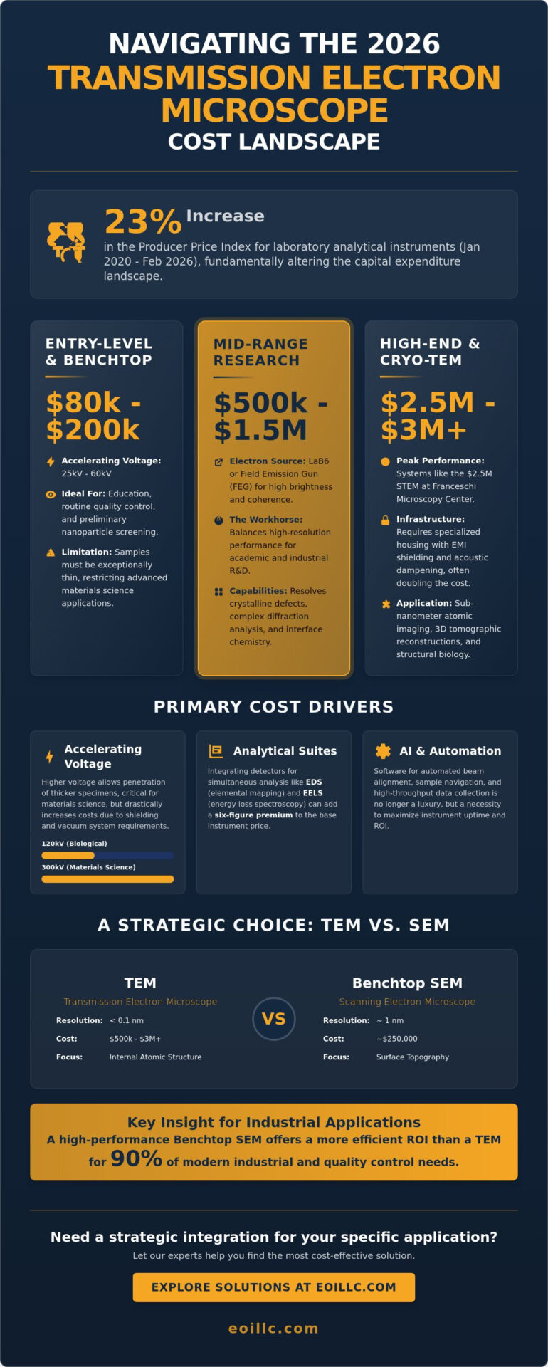
The Producer Price Index for laboratory analytical instruments increased by approximately 23% between January 2020 and February 2026, a shift that’s fundamentally altered the capital expenditure landscape for advanced imaging facilities. You’ve likely found that calculating the transmission electron microscope cost is no longer a straightforward budgetary exercise; this is particularly true when high-end systems like the scanning transmission electron microscope installed at the Franceschi Microscopy and Imaging Center in April 2026 now command a $2.5 million investment. This guide offers a comprehensive framework to navigate these volatile market tiers, ranging from $400,000 entry-level units to sophisticated cryo-TEM systems that often exceed $3 million. We’ll analyze the critical infrastructure requirements and specialized housing that frequently double the total cost of ownership. By the conclusion of this technical assessment, you’ll possess the precision tools necessary to determine if your research truly requires sub-nanometer transmission or if a high-performance $250,000 benchtop SEM represents a more strategic integration for your specific industrial applications.
Key Takeaways
- Categorize capital investments into entry-level, mid-range, and high-end tiers to align your budgetary allocation with specific sub-nanometer resolution requirements.
- Evaluate how specific technical parameters, such as accelerating voltage and electron source selection, act as primary drivers for the total transmission electron microscope cost.
- Account for essential infrastructure overheads, including electromagnetic interference shielding and acoustic dampening, to ensure the laboratory environment supports precision imaging.
- Utilize a strategic framework to determine when the 1nm resolution of a high-performance benchtop SEM offers a more efficient ROI than the 0.1nm capabilities of a traditional TEM.
- Discover how the evolution of benchtop microscopy, exemplified by the Cube II, provides a cost-effective alternative for 90% of modern industrial and quality control applications.
The 2026 Transmission Electron Microscope Price Landscape
The 2026 fiscal year has introduced unprecedented complexity into the procurement of high-end optical solutions. Transmission electron microscopy remains the definitive standard for sub-nanometer characterization, utilizing a high-energy electron beam that penetrates ultra-thin specimens to reveal internal atomic structures. Unlike scanning systems that focus on surface topography, the TEM provides a projection of the sample’s internal morphology. This capability makes it indispensable for semiconductor failure analysis and structural biology. However, the transmission electron microscope cost has been significantly influenced by a 23% increase in the Producer Price Index for laboratory analytical instruments recorded between 2020 and early 2026. This inflationary pressure, coupled with a surge in specialized, application-specific configurations, necessitates a tiered approach to capital investment. Organizations must evaluate their requirements against the broader electron microscope cost landscape to ensure technical alignment.
Entry-Level and Benchtop TEM Systems
Entry-level systems, often configured as benchtop or tabletop units, represent a strategic entry point for educational institutions and preliminary nanoparticle screening. These instruments typically command a price range between $80,000 and $200,000. While they offer significant accessibility, they operate with lower accelerating voltages, generally capped between 25kV and 60kV. This limitation dictates that samples must be exceptionally thin, often restricting their utility in advanced materials science where 200kV penetration is the baseline requirement. For organizations that don’t require atomic-scale lattice imaging, these compact units provide a reliable platform for routine quality control without the massive infrastructure overhead of floor-standing models.
Mid-Range and High-Resolution Research TEMs
Standard research-grade systems occupy the mid-range tier, with acquisition costs typically falling between $500,000 and $1.5 million. These floor-standing units are frequently equipped with Lanthanum Hexaboride (LaB6) or Field Emission Gun (FEG) sources, providing the brightness and coherence necessary for complex diffraction analysis. At this level, the transmission electron microscope cost reflects the integration of advanced analytical suites, including Energy Dispersive Spectroscopy (EDS) for elemental mapping. These systems represent the workhorse of modern academic and industrial R&D facilities. They balance high-resolution performance with versatile sample handling capabilities, allowing for the precise characterization of crystalline defects and interface chemistry that entry-level units cannot resolve.
Technical Factors Driving Transmission Electron Microscope Cost
The technical architecture of a TEM is the primary determinant of its market valuation. Accelerating voltage serves as a critical differentiator; systems operating at 200kV to 300kV require significantly more robust vacuum systems and radiation shielding than 100kV units. These high-voltage configurations allow for the penetration of thicker specimens, which is essential for 3D tomographic reconstructions and advanced materials science. Consequently, the electron microscopy market reflects a substantial price delta between standard 120kV biological models and 300kV materials science platforms. While a lower voltage might suffice for simple nanoparticle screening, the pursuit of atomic-scale resolution necessitates a higher energy beam, which fundamentally scales the total investment.
Analytical integration also drives the transmission electron microscope cost. Modern laboratories frequently require simultaneous elemental analysis through Energy Dispersive Spectroscopy (EDS) and Electron Energy Loss Spectroscopy (EELS). Integrating these dual analytical suites often adds a six-figure premium to the base instrument price. By 2026, the industry has also prioritized AI-driven automation. Software that manages automated beam alignment and high-throughput data collection is no longer a luxury but a necessity for facilities seeking to maximize instrument uptime and reproducibility. This shift toward “smart” microscopy ensures that even complex data sets can be captured with minimal manual intervention, though it adds to the initial software licensing fees.
The Impact of the Electron Gun Source
The choice of electron source dictates the instrument’s ultimate resolution and brightness. Tungsten filaments represent a legacy solution; they’re cost-effective but suffer from low brightness and require frequent replacement. In contrast, Field Emission Guns (FEG) provide the high coherence necessary for sub-nanometer characterization. The evolutionary shift toward cold-FEG technology in 2026 offers superior energy spread and stability. It’s a high-precision choice that demands more stringent ultra-high vacuum conditions and specialized maintenance protocols, which contributes to higher long-term operational expenses.
Detectors and Specialized Imaging Hardware
Imaging hardware has seen rapid advancements, particularly with the rise of Direct Electron Detectors. These sensors are vital for Cryo-EM applications where low-dose imaging is required to preserve sensitive biological structures. Adding such hardware, along with in-situ holders for observing real-time reactions under heat, liquid, or gas flow, can increase the total investment by 30% or more. For those seeking to optimize their laboratory capabilities without the extreme overhead of a full TEM installation, exploring high-performance scanning solutions may provide a more balanced investment strategy. High-speed cameras for dynamic event capturing also represent a significant capital outlay, as they’re required to process the massive data streams generated during in-situ experiments.
Hidden Infrastructure and Total Cost of Ownership (TCO)
Acquiring a high-resolution imaging system involves far more than the initial capital outlay for the instrument itself. Many organizations underestimate the secondary expenses, which frequently add 20% to 40% to the base transmission electron microscope cost. A TEM cannot function to its theoretical resolution limits in a standard laboratory environment. It requires a specialized “quiet” room that mitigates environmental interference. If these factors aren’t addressed during the planning phase, the resulting image instability can render a multi-million dollar investment ineffective. Beyond the physical housing, operational overhead including high power consumption and specialized vacuum pump maintenance creates a continuous budgetary demand that must be forecasted with precision.
Service and reliability are equally critical components of the TCO equation. Annual service agreements for these complex optical systems are mandatory to prevent catastrophic downtime. While similar in principle to standard sem maintenance, TEM support protocols are significantly more rigorous due to the higher accelerating voltages and more complex lens geometries involved. These contracts ensure the longevity of the electron source and the integrity of the vacuum seals, protecting the precision of the system over its evolutionary lifecycle.
Specialized Room Construction Requirements
The physical environment must be engineered to extreme tolerances. Thermal stability is paramount; most high-end systems require room temperatures to be maintained within a 0.1°C range to prevent thermal drift of the electron beam. Additionally, active vibration isolation systems are often necessary to decouple the instrument from floor tremors, especially in urban research hubs. Electromagnetic interference (EMI) shielding is another significant hidden expense. Specialized “quiet” rooms utilize Mu-metal or active cancellation coils to neutralize external magnetic fields that would otherwise deflect the electron path and blur atomic-scale details.
The Burden of Technical Expertise
Human capital represents a substantial ongoing investment. Operating a 200kV or 300kV TEM typically requires dedicated PhD-level staff to ensure data accuracy and instrument safety. According to 2026 service core data, unassisted scope time averages $68.74 per hour, while assisted sessions reach $99.75 per hour. Training costs are also significant; a single TEM training session in 2026 is priced at approximately $500. Sample preparation introduces further complexity and cost. Techniques like ultramicrotomy or Focused Ion Beam (FIB) milling are essential for creating the ultra-thin sections required for transmission. For instance, processing and embedding a set of 1 to 10 specimens currently commands a fee of $320.25, reflecting the specialized labor and consumables involved in the workflow.
TEM vs. SEM: A Strategic Cost-Benefit Comparison
Selecting the appropriate imaging modality requires a rigorous evaluation of both analytical requirements and capital efficiency. While the transmission electron microscope cost frequently exceeds $400,000 for entry-level units and reaches $2.5 million for advanced scanning transmission systems, the investment must be justified by the need for sub-nanometer internal characterization. In contrast, the scanning electron microscope price landscape offers a more accessible range. High-performance floor-standing SEMs typically command between $300,000 and $650,000, while benchtop alternatives provide significant utility starting at $80,000. The decision hinge point is often resolution; a TEM offers 0.1nm precision for atomic lattice imaging, but the 1nm resolution provided by modern Field Emission SEMs is sufficient for the vast majority of industrial applications.
Operational throughput further differentiates these platforms. Sample preparation for TEM is a high-precision, labor-intensive process that significantly increases billable hours. Creating the ultra-thin sections required for electron transparency often involves complex ultramicrotomy or Focused Ion Beam (FIB) milling, with specimen embedding alone costing approximately $320.25 per set. SEM preparation is comparatively streamlined, allowing for higher sample volumes and faster data acquisition. For facilities focused on surface morphology rather than internal atomic projection, the SEM provides a more favorable return on investment by reducing the total cost of ownership. To optimize your laboratory’s capital allocation, consider exploring high-resolution scanning solutions that bridge the gap between performance and price.
Industrial Failure Analysis: Choosing the Right Tool
In the semiconductor and automotive sectors, failure analysis often prioritizes surface topography and cross-sectional morphology. Modern FE-SEMs excel in these areas, providing the depth of field necessary to visualize complex 3D structures that a TEM might flatten into a 2D projection. However, when the research objective involves crystallography or the identification of crystalline defects at the atomic scale, the TEM remains an unavoidable necessity. The strategic challenge lies in identifying the specific point where the additional resolution of a TEM justifies the 400% increase in capital expenditure over a high-end benchtop SEM.
Budgetary Efficiency and Resource Allocation
Avoiding the “over-specification” trap is essential for sustainable laboratory management. Organizations often default to purchasing a TEM for tasks that a modern $250,000 benchtop SEM could handle with equal precision. By calculating the cost-per-image, facilities often find that the specialized housing and PhD-level operator requirements of a TEM make it unsustainable for routine tasks. For budget-constrained environments, refurbished floor-model SEMs or high-throughput benchtop units represent a high-value alternative, delivering near-floor-model performance without the million-dollar infrastructure burden associated with the current transmission electron microscope cost.
The Benchtop SEM: A High-Performance, Cost-Effective Alternative
The 2026 fiscal year has marked a definitive transition in the micro-characterization market. As the transmission electron microscope cost continues to escalate due to specialized optics and complex housing requirements, the desktop sem has emerged as a high-precision alternative for industrial and research workflows. Modern benchtop systems, such as the Cube II, provide a sophisticated integration of high-resolution imaging and elemental analysis within a compact footprint. This evolutionary shift allows laboratories to bypass the prohibitive capital expenditure associated with traditional TEM platforms while maintaining the analytical rigor required for advanced materials science. By eliminating the need for specialized “quiet” rooms or active vibration isolation systems, these instruments provide an immediate return on investment.
The synergy between high-resolution electron optics and integrated Energy Dispersive Spectroscopy (EDS) in a benchtop format has redefined laboratory efficiency. For organizations that don’t require the 0.1nm lattice imaging mentioned in previous sections, the Cube II offers near-floor-model performance at a fraction of the total cost of ownership. This accessibility doesn’t compromise quality; rather, it reflects a refinement in optical engineering that prioritizes practical utility and throughput. The ability to generate high-fidelity data without the million-dollar infrastructure burden of a TEM makes the benchtop SEM a logical choice for 90% of industrial quality control applications. It’s a strategic pivot that balances precision with fiscal responsibility.
Performance Evolution of Benchtop Systems
The technical capabilities of 2026 benchtop models now rival the resolution of floor-model SEMs from just ten years ago. This advancement is coupled with an intuitive user interface that reduces the reliance on high-cost, PhD-level operators. Rapid installation protocols allow these systems to be operational within hours of delivery. They offer a level of flexibility for evolving lab environments that stationary TEM installations simply cannot match. Because they don’t require liquid nitrogen or specialized high-power circuits, the ongoing operational overhead remains significantly lower than the standard transmission electron microscope cost.
The EOI Advantage in Electron Optics
EOI LLC leverages over 30 years of expertise in precision optics to assist partners in selecting the most strategic tool for their specific applications. Our commitment to excellence is reflected in the Genesis series and the Cube II, which are positioned as the benchmark for cost-conscious, high-performance research. We provide comprehensive service contracts that ensure long-term operational stability and precision. By focusing on sustainable innovation and technical authority, EOI LLC empowers global manufacturing leaders to achieve superior characterization results without the unnecessary complexity of over-engineered imaging platforms.
Strategizing Your Laboratory’s Evolutionary Path in 2026
The technical analysis presented here demonstrates that the transmission electron microscope cost is merely the foundational element of a broader total cost of ownership that encompasses specialized housing and PhD-level operational expertise. Organizations must weigh these requirements against the rising capabilities of modern benchtop systems, which now provide sufficient resolution for the majority of industrial applications. This strategic assessment ensures that your facility avoids the trap of over-specification while maintaining the precision necessary for competitive excellence. Selecting the right modality isn’t just about resolution; it’s about aligning capital expenditure with practical throughput and long-term reliability.
EOI LLC utilizes over 30 years of industry experience to assist partners in navigating these complex capital expenditure landscapes. As the exclusive US distributor for EmCraft systems and a provider of full-service support for all major electron microscope brands, we emphasize the synergy between innovation and global manufacturing capability. We invite you to consult with our experts to find the most cost-effective electron optics solution for your lab and secure a future defined by technical authority. Precision imaging is a strategic asset for success, and we’re here to ensure your investment delivers maximum value.
Frequently Asked Questions
How much does a new transmission electron microscope cost in 2026?
The transmission electron microscope cost in 2026 ranges from $400,000 for entry-level models to over $3,000,000 for high-end aberration-corrected or cryo-EM systems. A specific example of current market valuation is the scanning transmission electron microscope installed at the Franceschi Microscopy and Imaging Center in April 2026, which required a $2.5 million investment. These price points reflect a 23% increase in laboratory analytical instrument costs since January 2020.
What is the difference between TEM and SEM in terms of price?
TEM systems typically command a 300% to 500% price premium over scanning electron microscopes due to their more complex high-voltage architecture. While a high-performance benchtop SEM is priced between $80,000 and $250,000, an entry-level TEM starts at approximately $400,000. Mid-range floor-standing FE-SEMs generally peak at $650,000, whereas mid-range research TEMs often reach $1.5 million.
Why are transmission electron microscopes so expensive compared to optical ones?
The cost disparity is driven by the precision engineering required to generate and focus electron beams at accelerating voltages up to 300kV. Unlike optical microscopes that use glass lenses and ambient air, a TEM requires ultra-high vacuum chambers and sophisticated electromagnetic lenses to achieve sub-nanometer resolution. This complex internal environment is necessary to bypass the diffraction limits of visible light.
What are the hidden costs of installing a TEM?
Hidden infrastructure expenses frequently add 20% to 40% to the initial purchase price of the instrument. These include the construction of specialized “quiet” rooms featuring Mu-metal shielding for electromagnetic interference and active vibration isolation systems. You must also budget for rigorous HVAC controls capable of maintaining thermal stability within 0.1°C to prevent beam drift during high-resolution imaging.
Can a benchtop SEM replace a TEM for most research applications?
A high-performance benchtop SEM can replace a TEM for approximately 90% of industrial quality control and failure analysis tasks where 1nm resolution is sufficient. TEM technology remains an absolute necessity only when the research objective requires internal atomic lattice projection or advanced crystallography. For surface morphology and cross-sectional analysis, the benchtop SEM provides a more strategic and cost-effective integration.
How much should I budget for annual TEM maintenance?
Annual maintenance budgets should ideally represent 10% to 15% of the instrument’s original capital expenditure. This allocation covers essential service contracts, vacuum pump maintenance, and the periodic replacement of electron sources. Given that assisted staff time for microscopy services in 2026 can reach $170 per hour, a comprehensive service agreement is vital for managing long-term operational overhead.
Is it better to buy a refurbished electron microscope to save on costs?
Purchasing a refurbished system is a viable strategy for laboratories with significant budget constraints that still require high-resolution capabilities. These units often deliver near-modern performance when sourced from reputable providers like EOI LLC. It’s critical to ensure the refurbished unit includes a modern digital imaging suite and a guaranteed service contract to maintain operational stability over its remaining lifecycle.
What infrastructure is required for a high-resolution TEM?
High-resolution TEM requires an ultra-low vibration environment, often necessitating a reinforced ground-floor slab decoupled from the rest of the building. Acoustic dampening and electromagnetic shielding are mandatory to protect the electron path from external interference. Additionally, the facility must provide stable, high-capacity electrical power and specialized cooling water loops to manage the heat generated by the electromagnetic lenses.