
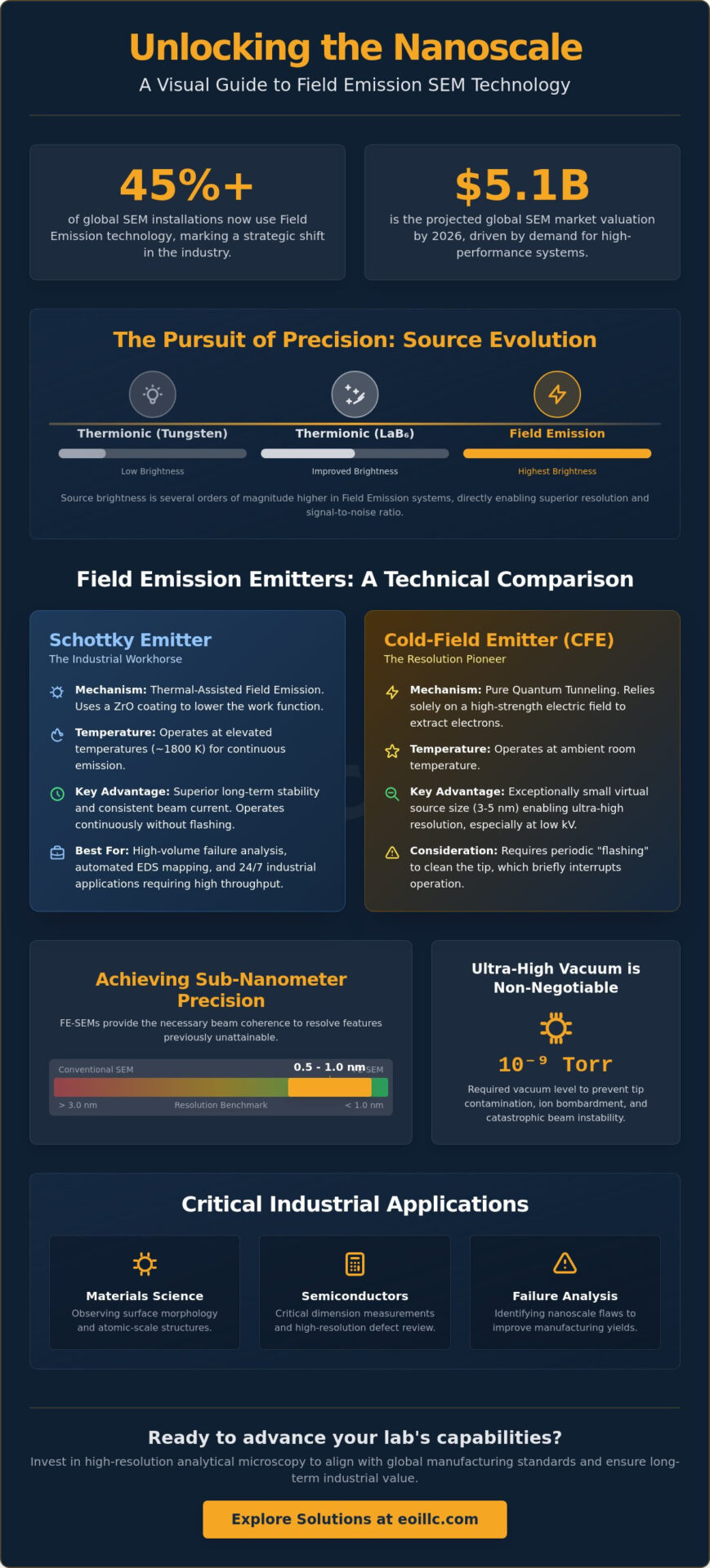
The transition from simple imaging to precision characterization is no longer a luxury but a strategic necessity in an industry where field emission technology now accounts for over 45% of global installations. As the global scanning electron microscope market accelerates toward a projected $5.10 billion valuation in 2026, the demand for a high-performance field emission scanning electron microscope has become paramount for organizations targeting sub-nanometer precision. You’ve likely experienced the limitations of insufficient resolution when documenting nanoscale features or the operational delays caused by sample damage under high beam currents. We recognize that slow throughput in failure analysis workflows represents a significant barrier to industrial excellence.
This article provides a comprehensive analysis of the mechanics and industrial advantages inherent in field emission technology. You’ll gain a technical understanding of the distinction between Schottky and Cold-Field emitters while exploring how recent advancements, such as the JEOL JSM-IT810 released in July 2024, redefine throughput standards. We’ll conclude by evaluating the strategic ROI of high-resolution analytical microscopy to ensure your laboratory’s evolutionary trajectory remains aligned with global manufacturing standards and the rigorous demands of sub-nanometer characterization.
Key Takeaways
- Differentiate between thermionic and field-based electron sources to understand the fundamental mechanics behind superior beam coherence and precision.
- Compare the physics of Schottky and Cold-Field emission to select the emitter type that best supports your laboratory’s specific stability and resolution requirements.
- Achieve imaging benchmarks between 0.5nm and 1.0nm by leveraging a field emission scanning electron microscope for your most demanding nanoscale characterization tasks.
- Explore how high-resolution imaging facilitates critical dimension measurements and defect reviews within the semiconductor and materials science industries.
- Assess strategic implementation factors like maintenance uptime and analytical integration to ensure your equipment investment delivers long-term industrial value.
Defining the Field Emission Scanning Electron Microscope (FE-SEM)
A field emission scanning electron microscope represents the current apex of electron optics, utilizing a field emission gun to generate an electron beam characterized by extreme narrowness and high spatial coherence. This technology differs fundamentally from conventional SEMs that rely on thermionic emission, where a tungsten filament is heated until electrons overcome the material’s work function. Instead, field emission utilizes a high-strength electric field to extract electrons from a sharp tungsten tip through quantum tunneling. This shift from thermal energy to field-assisted extraction is what enables the precision required for sub-nanometer characterization in 2026. Industrial excellence now demands this level of resolution as miniaturization in the semiconductor and materials science sectors reaches the atomic scale.
The operational architecture of a high-performance system integrates several critical components to achieve these results. These include the field emission source itself, a complex arrangement of electromagnetic lenses for beam focusing, and a specialized ultra-high vacuum system. By producing a probe diameter that is significantly smaller than that of a thermionic source, the field emission scanning electron microscope allows researchers to observe surface morphology with a depth of field and clarity that was previously unattainable.
The Evolution of Electron Sources
The trajectory of electron microscopy has been defined by a relentless pursuit of higher source brightness. Early systems utilized tungsten filaments, which were eventually supplemented by lanthanum hexaboride crystals to improve beam stability. However, the transition to field emission tips marked a definitive evolutionary leap in optical performance. Brightness in the context of electron optics is defined as a measure of current density per solid angle. Because field emission tips provide brightness levels several orders of magnitude higher than their predecessors, they directly dictate the ultimate resolution and signal-to-noise ratio of the final image.
Why Ultra-High Vacuum (UHV) is Non-Negotiable
Maintaining an ultra-high vacuum environment is a non-negotiable requirement for the operational integrity of a field emission source. Gas molecules present in the column can collide with the delicate tip or cause ion bombardment, leading to rapid contamination and catastrophic beam instability. To prevent these failures, modern systems utilize dedicated ion pumps to maintain vacuum levels at or below 10^-9 Torr. This rigorous environmental control ensures the long-term reliability of the electron source and the consistency of high-resolution analytical workflows across global manufacturing chains. It’s this synergy between vacuum science and electron physics that underpins the stability of the modern laboratory.
Schottky vs. Cold-Field Emission: Technical Mechanisms
The operational efficacy of a field emission scanning electron microscope is fundamentally dictated by the architecture of its electron source, with the industry bifurcated between Cold-Field Emission (CFE) and Schottky emitters. While both technologies utilize high-strength electric fields, their physical mechanisms for electron extraction diverge significantly. CFE guns operate at ambient temperatures, relying exclusively on quantum tunneling to liberate electrons from a mono-crystalline tungsten tip. This process produces an exceptionally small virtual source size, typically measuring between 3 and 5 nanometers, which is the primary driver for ultra-high-resolution imaging at low accelerating voltages.
Conversely, Schottky emitters represent a hybrid approach known as thermal-assisted field emission. These sources utilize a zirconium oxide coating on the tungsten tip to lower the material’s work function, allowing for continuous electron emission at elevated temperatures. This architectural difference has profound implications for laboratory throughput. While CFE tips require periodic flashing, which is a process of heating the tip to remove adsorbed gas molecules that disrupt the beam, Schottky sources operate continuously with superior long-term stability. For organizations managing high-volume failure analysis or automated EDS mapping, the consistent current of a system like the Veritas FE SEM provides the reliability required for 24/7 industrial operations.
Cold-Field Emission (CFE) for Ultimate Resolution
CFE technology is the preferred choice for research environments where sub-nanometer resolution is the absolute priority. By minimizing the energy spread of the emitted electrons, CFE sources reduce chromatic aberration, which is essential for characterizing delicate nanostructures. However, the trade-off involves a lower total beam current and a susceptibility to current fluctuations over time. This makes CFE ideal for specialized nanotechnology characterization where the pursuit of precision outweighs the need for high-speed analytical throughput.
Schottky Emitters: The Industrial Workhorse
Schottky systems have emerged as the industrial standard for the modern field emission scanning electron microscope because they balance high-resolution capabilities with high probe currents. This synergy is critical for analytical techniques such as Energy Dispersive Spectroscopy (EDS) and Electron Backscatter Diffraction (EBSD). As evidenced by the release of the JEOL JSM-IT810 on July 28, 2024, Schottky technology continues to dominate the market for automated observation and analysis. Because these emitters don’t require the frequent downtime associated with tip flashing, they’re perfectly suited for automated workflows and large-area mapping. This stability ensures that the integration of AI-assisted image analysis remains accurate over extended sessions, reflecting the evolutionary shift toward more autonomous manufacturing diagnostics.
FE-SEM vs. Conventional SEM: Resolution and Performance
The performance gap between a field emission scanning electron microscope and a conventional thermionic system is best illustrated through the lens of resolution and source brightness. While a standard tungsten filament system typically struggles to achieve resolutions finer than 3.0 nanometers, a high-performance FE-SEM routinely delivers benchmarks between 0.5 nanometers and 1.0 nanometers. This precision isn’t merely a marginal gain. It represents a fundamental shift in analytical capability. The field emission source provides a beam that is 100 to 1,000 times brighter than those produced by thermionic sources. This intensity allows for a smaller probe size at the sample surface, which is the primary driver for ultra-high-resolution imaging in modern industrial environments.
Beyond raw resolution, the field emission scanning electron microscope offers a superior depth of field. This is critical when capturing complex 3D topographies at magnifications exceeding 100,000x. In industrial failure analysis, where the goal is often to identify sub-micron fractures or structural anomalies, the coherence of the field emission beam ensures that the entire surface remains in focus. This visual depth provides a level of clarity that thermionic systems cannot replicate, particularly when navigating the intricate geometries of modern semiconductors or advanced composite materials that define the technological landscape of 2026.
Imaging Beam-Sensitive Materials
The capability to operate effectively at low accelerating voltages is perhaps the most significant advantage of FE-SEM technology. Conventional systems often require high kilovolt (kV) settings to maintain a stable signal, which frequently results in sample charging or the destruction of delicate specimens. By contrast, field emission systems maintain high brightness even at low kV, making them indispensable for imaging non-conductive and beam-sensitive materials like polymers, biological samples, and advanced thin films. For a detailed exploration of these specialized workflows, consult our guide on high resolution sem imaging techniques.
Analytical Capabilities and EDS Integration
High beam brightness does more than improve image quality; it fundamentally enhances chemical analysis through Energy Dispersive Spectroscopy (EDS). Because the field emission source generates a higher current density within a smaller spot, it produces a significantly improved signal-to-noise ratio. This synergy allows for faster mapping speeds and more accurate element identification without sacrificing spatial resolution. In a production environment, this translates to higher throughput. Operators can achieve detailed compositional maps in a fraction of the time required by older systems, a critical factor for maintaining supply chain excellence and rigorous quality control standards.
Critical Industrial Applications of FE-SEM Technology
Industrial leadership in 2026 relies on the ability to visualize and quantify features once considered beyond the reach of standard electron optics. The field emission scanning electron microscope has transitioned from a specialized research tool to a cornerstone of global manufacturing and quality assurance. Within the semiconductor sector, the shift toward the 5nm node and below has rendered traditional imaging methods obsolete. Engineers now utilize FE-SEM for critical dimension (CD) measurements and defect review, ensuring that lithographic patterns maintain their integrity across complex multilayer architectures. This precision is essential for maintaining high yield rates in an environment where even a single sub-micron anomaly can compromise an entire production batch.
Material science and metallurgy also benefit from this evolutionary leap in imaging capability. Characterizing carbon nanotubes, graphene, and catalyst particles requires the ultra-high resolution that field emission sources deliver. In metallurgical applications, the ability to analyze grain boundaries and precipitate morphology at the atomic scale facilitates the engineering of advanced alloys with superior thermal and mechanical properties. These capabilities allow organizations to push the boundaries of what’s possible in sustainable innovation and high-end manufacturing. Identifying the root cause of microscopic cracks or surface contamination early in the development cycle prevents catastrophic failures in the field.
Precision Failure Analysis Workflows
Identifying the root cause of microscopic cracks or surface contamination requires a methodical approach to imaging. By utilizing a field emission scanning electron microscope, failure analysis teams can perform detailed cross-sectional analysis for multilayer thin-film characterization. This level of scrutiny is vital for identifying manufacturing defects that occur at the sub-micron level. For a deeper understanding of how these techniques are applied in industrial settings, please refer to our failure analysis sem guide. Organizations looking to integrate these capabilities into their own facilities can explore our range of high-performance analytical solutions to find the optimal system for their specific requirements.
Nanotechnology and Nanofabrication
The synthesis of nanomaterials for drug delivery and energy storage relies on the constant monitoring of particle size and distribution. As nanofabrication moves toward molecular-scale engineering, the role of FE-SEM becomes increasingly central to the development process. Verifying the integrity of lithographic patterns at the 5nm node requires the beam stability and brightness discussed in previous sections. This ensures that every component, from high-capacity batteries to advanced semiconductors, meets the rigorous standards of modern excellence. It’s this synergy between imaging precision and industrial performance that defines the current technological era.
Strategic Implementation: Selecting an FE-SEM for Your Lab
Implementing a field emission scanning electron microscope requires a rigorous evaluation of both capital expenditure and long-term operational viability. With new systems currently priced between $300,000 and over $1,000,000, as seen in recent 2026 market data, the initial investment is substantial. However, the true strategic value lies in calculating the total cost of ownership over a typical seven-year lifecycle. This calculation must account for maintenance uptime, throughput efficiency, and the specific analytical requirements of your facility. In an era where the global SEM market is projected to reach $5.10 billion by the end of 2026, the cost of unplanned downtime in a high-volume manufacturing environment can quickly exceed the initial purchase price of the equipment.
The Veritas FE SEM series is engineered to act as a bridge between high-end electron optics and practical laboratory efficiency. By integrating advanced Schottky emitters with streamlined software interfaces, these systems provide the sub-nanometer precision discussed in previous sections without the prohibitive complexity often associated with field emission technology. Selecting the right configuration involves a careful balance. You must determine if your workflows demand the ultimate resolution of a cold-field emitter for pure research or the analytical stability of a Schottky source for extensive EDS integration and automated failure analysis. The Veritas FE SEM, provided by Electron Optics Instruments, LLC, serves as an evolutionary anchor for labs transitioning from thermionic systems, providing a stable platform for sustainable innovation and global manufacturing excellence.
The Role of Preventative Maintenance
Field emission systems demand a more stringent maintenance schedule than their tungsten counterparts, primarily due to the sensitivity of the ultra-high vacuum environment. Maintaining 10^-9 Torr levels requires consistent monitoring of ion pumps and frequent aperture cleaning to prevent beam drift. Neglecting these protocols can lead to premature tip degradation, which significantly increases operational costs. For a comprehensive strategy on protecting your investment, read our sem maintenance guide, which outlines the protocols necessary for maximizing precision and longevity through 2026.
On-Site Training and Technical Support
The transition to a field emission scanning electron microscope often necessitates a shift in staff expertise. The sensitivity of field emission sources to environmental vibrations and electromagnetic interference means that proper installation and ongoing training are critical for achieving rated resolution. Expert relocation and calibration services ensure that the system achieves its theoretical limits from the moment of installation. If you’re ready to enhance your facility’s analytical capabilities with a partner that values precision and reliability, contact Electron Optics Instruments, LLC for a strategic consultation on the Veritas FE SEM series and our comprehensive technical support packages.
Advancing Industrial Precision Through 2026
The integration of a field emission scanning electron microscope into your analytical framework represents a definitive commitment to sub-nanometer precision and industrial excellence. By mastering the distinctions between Schottky and cold-field emission mechanisms, organizations can align their imaging capabilities with the rigorous demands of semiconductor node transitions and advanced material characterization. Success in this high-resolution landscape depends not only on the acquisition of high-performance optics but also on the implementation of methodical maintenance and expert technical support. It’s this synergy between technical prowess and global capability that ensures long-term operational reliability.
Electron Optics Instruments, LLC leverages over 30 years of electron microscopy expertise to support your facility’s evolutionary growth. As the sole US distributor for EmCraft Scanning Electron Microscopes and a provider of comprehensive service contracts for all major SEM brands, we ensure your operations maintain maximum uptime and accuracy. We invite you to explore the Veritas FE SEM and our full range of high-resolution solutions to secure your position at the forefront of global manufacturing. Your pursuit of atomic-scale clarity deserves a partner dedicated to technical authority and visionary innovation.
Frequently Asked Questions
What is the primary difference between SEM and FE-SEM?
The fundamental distinction lies in the electron source and the mechanism used to generate the beam. While a conventional SEM utilizes thermionic emission from a heated tungsten filament, a field emission scanning electron microscope extracts electrons through a high-strength electric field. This process results in a beam that’s 100 to 1,000 times brighter than thermionic sources, allowing for significantly higher resolution and a smaller probe size at the sample surface.
How long does a field emission tip typically last?
Field emission tips offer a significantly longer operational lifespan compared to the 100 hours typical of tungsten filaments. A Schottky emitter generally maintains its performance for 1 to 3 years under continuous high-vacuum operation. Cold-field emitters can last over 5 years, provided the vacuum integrity is never compromised. This longevity reduces the frequency of source replacements and minimizes system downtime in high-throughput industrial environments.
Why does an FE-SEM require an ultra-high vacuum system?
Ultra-high vacuum is essential to protect the delicate geometry of the emission tip from contamination and ion bombardment. Gas molecules present in a lower-quality vacuum can collide with the sharp tungsten tip or cause beam scattering, which degrades image resolution and stability. Maintaining pressure levels at 10^-9 Torr ensures the electron extraction remains consistent and prevents the catastrophic failure of the field emission gun during sensitive analytical sessions.
Can an FE-SEM image non-conductive samples without coating?
Yes, these systems excel at imaging non-conductive samples by utilizing low accelerating voltages. By operating at 0.1kV to 1kV, the microscope achieves a state of charge balance where the number of incident electrons equals the number of emitted electrons. This capability allows researchers to observe polymers and biological specimens in their native state without the need for gold or carbon coatings that might obscure fine surface details.
Is a Schottky emitter better than a Cold-Field emitter for my lab?
The choice between emitter types depends on whether your priority is analytical throughput or ultimate resolution. Schottky emitters are the preferred choice for 70% of industrial applications because they provide high beam current and superior long-term stability for EDS and EBSD mapping. Cold-field emitters are better suited for specialized nanotechnology research where achieving the absolute limit of sub-nanometer resolution is more critical than high-speed chemical analysis.
What is the typical resolution limit of a modern FE-SEM in 2026?
Current benchmarks for high-performance systems now reach between 0.5nm and 0.8nm at optimal accelerating voltages. Recent releases, such as the Zeiss GeminiSEM 450 introduced in January 2026, demonstrate the industry’s ability to resolve features that were previously invisible to all but the most advanced transmission microscopes. This level of precision is vital for verifying lithographic patterns and characterizing advanced materials at the atomic scale.
How much floor space and infrastructure does an FE-SEM require?
A standard installation requires approximately 10 to 15 square meters of dedicated laboratory space to accommodate the microscope, its electronics rack, and the operator workstation. Infrastructure requirements include specialized electromagnetic interference (EMI) shielding and active vibration damping tables to prevent environmental noise from blurring high-magnification images. Proper acoustic insulation is also necessary to maintain the stability required for imaging at magnifications exceeding 500,000x.
What are the maintenance requirements for a field emission electron gun?
Maintenance focuses on preserving the vacuum environment and ensuring the integrity of the high-vacuum apertures. Unlike tungsten systems that require frequent filament changes, a field emission scanning electron microscope requires annual preventative maintenance visits to evaluate ion pump health and bake out the column. Regular cleaning of the final apertures and periodic calibration using NIST standard reference materials, such as RM 8090, ensure the system maintains its precision over its multi-year lifecycle.