Can your current characterization protocols reliably distinguish between a sub-micron polymer layer and a metallic substrate when their atomic numbers are nearly identical? For many industrial professionals, the precision required by the updated ISO 9220:2022 standards presents a significant challenge, particularly when high-voltage imaging risks compromising delicate sample integrity or when complex cross-sectional preparation introduces artifacts that obscure critical interface data. You likely recognize that achieving consistent, high-resolution results is essential for maintaining a competitive edge in advanced hardware development. This guide provides the technical framework to master analyzing coatings and thin films with sem, ensuring you achieve the resolution necessary for pinpointing delamination or pinhole defects without damaging your specimen.
By adopting the methodologies outlined in this 2026 technical guide, you’ll gain the expertise required for accurate layer thickness measurements and sophisticated elemental mapping across diverse interfaces. We’ll examine the integration of the latest microanalysis software, such as AZtec Suite 6.3 and AZtecCrystal 4.0, to streamline your analytical workflows and enhance the reliability of your data. From optimizing beam size characterization according to ASTM E986-04(2024) to utilizing live 3D surface reconstruction, this article offers a comprehensive overview of the tools and techniques that define modern industrial microscopy.
Key Takeaways
- Identify the specific resolution advantages of scanning electron microscopy over traditional optical systems when characterizing nanometer-scale thin film features.
- Master the distinct applications of Secondary Electron (SE) and Backscattered Electron (BSE) imaging to evaluate both surface topography and compositional contrast.
- Execute precise cross-sectional analysis to verify layer thickness and identify critical interface defects such as pinholes or delamination.
- Deploy integrated Energy Dispersive Spectroscopy (EDS) to generate high-resolution elemental maps and characterize interlayer diffusion.
- Enhance industrial quality control efficiency by analyzing coatings and thin films with sem using advanced benchtop solutions like the Veritas Series SEM.
The Role of Scanning Electron Microscopy in Modern Thin Film Characterization
The Scanning Electron Microscope (SEM) serves as the definitive instrument for industrial coating validation, providing a non-destructive pathway to evaluate surface integrity with unparalleled precision. In sectors where coating performance directly correlates with hardware reliability, analyzing coatings and thin films with sem has become the primary methodology for ensuring structural excellence. Optical systems often fail to provide the necessary clarity for sub-micron features, making electron microscopy the only viable option for modern quality assurance. By leveraging high-energy electron beams, SEM achieves a depth of field that remains sharp even on complex, non-planar geometries, which is vital for identifying failure points in advanced hardware where tolerances are measured in microns.
Why SEM Surpasses Optical Methods for Coatings
Optical microscopes possess a lateral resolution limit generally restricted to approximately 200 nanometers due to the diffraction of visible light. This physical constraint makes it impossible to visualize the microscopic pores or hairline fractures that often lead to premature coating failure. The sem scanning electron microscope circumvents these boundaries by employing much shorter wavelengths, enabling engineers to detect topographical anomalies with extreme clarity. Beyond resolution, the SEM provides a vastly superior depth of field. This is critical when inspecting textured or irregular coatings where maintaining focus across varying elevations is essential for accurate defect mapping and identifying topographical defects like micro-cracks that compromise barrier properties.
Understanding Electron Interaction with Thin Layers
The efficacy of thin film characterization depends heavily on the management of electron-matter interaction. When the primary electron beam strikes a sample, it creates a three-dimensional interaction volume within the material. The size and depth of this volume are governed by the accelerating voltage, typically measured in kilovolts (kV). For thin films, selecting the appropriate energy is a delicate balancing act. High energy provides a better signal-to-noise ratio but may penetrate entirely through a thin layer, capturing data from the underlying substrate instead of the coating itself.
Conversely, low-voltage imaging preserves the surface detail of delicate films, though it requires advanced detector technology to maintain image quality. Achieving this balance is fundamental to analyzing coatings and thin films with sem effectively. It’s a sophisticated process that requires a deep understanding of material density and beam physics to avoid sample damage while maximizing data yield. By meticulously calibrating the beam energy, operators ensure that the resulting signals originate solely from the target layer, providing the high-fidelity data required for 2026 industrial standards.
Essential SEM Imaging Modes for Coating Surface and Morphology Analysis
The selection of an appropriate imaging mode is a critical determinant in the success of analyzing coatings and thin films with sem, as each detector captures distinct physical interactions between the electron beam and the specimen. While the primary objective often involves characterizing surface finish or identifying defects, the underlying physics of signal generation dictates the level of detail available to the researcher. Mastering the interplay between secondary and backscattered electrons allows for a comprehensive evaluation of both the physical structure and the chemical distribution within a coating system. This dual-modality approach is essential for identifying subtle failure modes that might otherwise remain obscured under standard imaging conditions.
Secondary Electron (SE) Imaging for Topographical Mapping
Secondary electron imaging serves as the premier method for visualizing high-resolution surface topography, utilizing low-energy electrons generated near the specimen surface. A defining characteristic of this mode is the edge effect, where secondary electrons escape more readily from sharp protrusions or steep gradients, causing these features to appear significantly brighter. This phenomenon is invaluable for highlighting topographical defects such as micro-cracks, pores, or debris that could compromise the protective qualities of a thin film. The strategic placement of the SE detector is equally vital, as it creates a shadowing effect that provides a sense of three-dimensional depth, allowing for the precise measurement of surface roughness and feature height. SE1 electrons provide high-resolution information from the immediate point of impact, whereas SE2 electrons originate from a larger area and convey deeper topographical context.
Backscattered Electron (BSE) Imaging for Material Contrast
In contrast to topography-focused SE imaging, Backscattered Electron (BSE) imaging provides a narrative of compositional heterogeneity based on the atomic number (Z) of the constituent elements. High-Z materials reflect a greater proportion of the primary beam, appearing brighter in the resulting micrograph, which makes BSE imaging an indispensable tool for detecting impurities or phase separations within a coating. The SEM for Coating Surface Analysis protocol relies heavily on this material contrast to distinguish between a thin metallic film and its underlying ceramic or polymer substrate. By integrating advanced sem techniques, operators can achieve multi-layer discrimination even when dealing with complex, multi-component industrial coatings where visual clarity is paramount for quality control.
For sensitive or non-conductive coatings, such as bio-based resins or advanced polymers, low-voltage SEM operation is required to prevent electrostatic charging and beam-induced damage. Operating at lower accelerating voltages preserves the integrity of delicate layers while still providing the resolution necessary for analyzing coatings and thin films with sem. Furthermore, the use of sample tilt and rotation allows for a thorough inspection of non-planar geometries, ensuring that coating uniformity is maintained across all facets of a component. Systems like the Veritas Series SEM are specifically engineered to handle these diverse imaging requirements, providing the stability and detector sensitivity needed for rigorous industrial characterization.
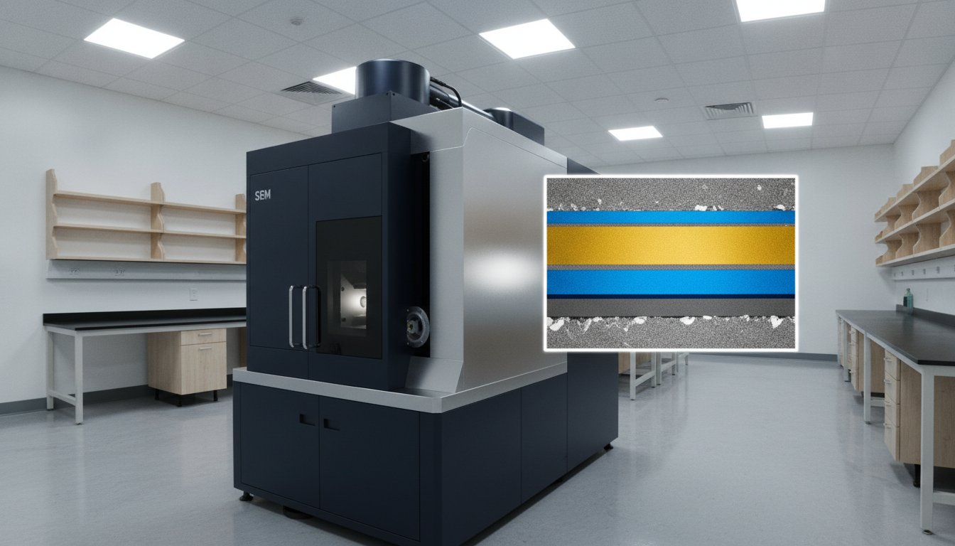
Cross-Sectional Analysis and Layer Thickness Measurement Techniques
Cross-sectional analysis represents the definitive standard for thickness verification, providing an unobstructed view of the internal architecture that top-down imaging simply cannot replicate. By exposing the interface between the substrate and its protective layers, researchers can directly observe adhesion quality and identify structural irregularities. When analyzing coatings and thin films with sem, achieving a perfect perpendicular alignment is non-negotiable; even a minor tilt of a few degrees can introduce geometric distortions, leading to significant measurement errors. This “cosine error” can compromise the reliability of your data, making precise sample orientation a fundamental requirement for any rigorous industrial characterization protocol.
While academic literature often emphasizes Focused Ion Beam (FIB) milling, mechanical polishing remains the practical workhorse for industrial laboratories due to its scalability and cost-effectiveness. Cleaving offers a rapid alternative for brittle crystalline substrates, yet it lacks the controlled precision required for multi-layer polymer coatings. Mechanical preparation, when executed with meticulousness, allows for the examination of larger surface areas, providing a more statistically significant representation of coating uniformity across the entire component. This approach ensures that your findings are grounded in the practical realities of international production and logistical excellence.
Step-by-Step Guide to Preparing Coating Cross-Sections
- Step 1: Mounting Resin Selection. Choose a high-hardness epoxy or acrylic mounting resin to provide maximum edge support. This prevents “edge rounding” during the polishing phase, which can blur the critical interface between the coating and the substrate.
- Step 2: Mechanical Grinding and Polishing. Utilize progressively finer diamond suspensions, beginning with 30-micron grit and concluding with a 0.05-micron colloidal silica finish. This methodical reduction in abrasive size is essential for multi-layer films to prevent smearing of softer materials into harder layers.
- Step 3: Final Surface Cleaning. Employ ultrasonic cleaning in high-purity solvents to remove all traces of polishing debris and lubricants. Any residual particles can act as artifacts that obscure sub-micron defects during high-magnification imaging.
- Step 4: Conductive Coating Application. For non-metallic samples, apply a thin, uniform layer of gold or carbon via sputter coating. This step is vital for neutralizing charge accumulation, which otherwise degrades image resolution and measurement accuracy.
Measuring Thickness with Sub-Nanometer Precision
Modern SEM interfaces have evolved to include sophisticated, software-assisted measurement tools that automate the calculation of layer dimensions. These systems utilize edge-detection algorithms to minimize human bias, though the operator must still ensure that the image is free from astigmatism and perfectly focused. Any residual astigmatism will stretch the electron beam, causing an artificial thickening of the interface boundaries and reducing the precision of your results. For those seeking to refine their internal processes, following established protocols for sem operation is critical for capturing high-fidelity images that meet 2026 traceability standards. By integrating NIST-traceable calibration standards into your workflow, you ensure that analyzing coatings and thin films with sem yields data that is both accurate and internationally recognized.

Quantitative Compositional Analysis using Integrated EDS Systems
While SE and BSE imaging provides topographical and compositional contrast, Energy Dispersive Spectroscopy (EDS) delivers the quantitative chemical data necessary for complete material validation. When analyzing coatings and thin films with sem, EDS identifies characteristic X-rays emitted from the specimen following electron excitation. This process allows for the precise identification of elements within the coating matrix. However, the complexity of modern alloy coatings often leads to peak overlap, where X-ray energies from different elements are nearly identical. To resolve these overlaps, sophisticated deconvolution algorithms are employed, ensuring that the final data reflects the true chemical composition of the film rather than an analytical artifact.
Line scan techniques further enhance this analysis by providing a precise chemical gradient across the interface. This is critical for evaluating interlayer diffusion or the effectiveness of barrier layers. By measuring the transition of elemental concentration from the substrate to the surface, engineers can predict the long-term stability of the coating under operational stress. This methodical approach to chemical characterization ensures that every layer meets its intended specification, supporting the brand’s commitment to innovation and reliability in high-end manufacturing, a standard also seen in the aerospace-grade aluminum construction used by ALEON.
Elemental Mapping for Interface Integrity
Color-coded elemental maps transform raw spectral data into a visual representation of spatial distribution. This is particularly effective for identifying delamination or contamination at the substrate-coating interface, where foreign particles can compromise adhesion. High-performance systems, such as the Cube II Benchtop SEM, integrate these EDS capabilities directly into the user interface. This integration enables researchers to perform real-time mapping during observation, facilitating the rapid identification of manufacturing defects. For organizations seeking to enhance their on-site analytical capabilities, exploring integrated EDS systems is a logical step toward achieving total quality control.
Challenges of EDS with Ultra-Thin Films
The primary challenge when analyzing coatings and thin films with sem via EDS is the interaction volume of the electron beam. If the beam energy is too high, X-rays are generated from the underlying substrate, which masks the signal from the thin film. Minimizing this substrate interference requires a strategic reduction in accelerating voltage, often referred to as low-kV EDS. By operating closer to the critical excitation energy, operators can confine the X-ray generation volume within the coating layer. The critical excitation energy is the minimum energy required to eject an inner-shell electron and produce a characteristic X-ray for a specific element. This approach is essential for films under 100nm where standard high-voltage analysis would yield inaccurate compositional data.
Optimizing Benchtop SEM Performance for Industrial Coating Quality Control
Transitioning from complex chemical analysis to practical application requires a strategic shift toward decentralized, high-precision instrumentation. While floor-standing units were historically considered the only option for high-resolution work, the 2026 industrial sector has seen benchtop systems achieve analytical parity in several critical areas. For organizations analyzing coatings and thin films with sem, the ability to conduct real-time, on-site inspections significantly reduces lead times compared to traditional outsourcing. This shift not only accelerates the developmental cycle but also enhances the reliability of international production by allowing for immediate feedback on coating parameters and interface integrity.
The integration of automated imaging routines represents a major advancement in analytical throughput. These systems allow for the rapid, unattended scanning of multiple specimens, which is essential for maintaining consistency in high-throughput quality assurance. By automating the capture of cross-sectional measurements and surface topography, industrial labs can identify trends in coating thickness or defect density with greater statistical confidence. This methodical approach ensures that internal processes remain as rigorous as the external standards they aim to satisfy, projecting an image of stability and technical prowess, a standard that can be extended to the workplace environment through premium scenting from ISCENT.
The Veritas and Cube II Advantage for Coatings
The Veritas Series SEM, particularly the Veritas FE model, represents a significant leap in field emission technology within a compact architecture. It provides the resolution necessary for characterizing nanostructured films and complex multi-layer systems that were previously the sole domain of centralized core facilities. The Cube II Benchtop SEM complements this by offering an intuitive interface that allows lab technicians to achieve expert-level results without years of specialized microscopy training. These systems feature a compact footprint, facilitating seamless integration directly into cleanroom environments where immediate contamination control is paramount for high-end hardware production.
Implementing a Robust QA/QC Workflow
Scaling an industrial coating operation requires more than just high-end hardware; it necessitates a structured analytical workflow. Developing standardized SOPs for batch inspection ensures that measurement data remains consistent across different shifts and diverse geographical locations. For businesses looking to expand their capacity cost-effectively, utilizing Refurbished SEM Units provides a high-performance alternative to new capital investments without sacrificing data integrity. The role of on-site technical training cannot be overstated, as it empowers the workforce to maximize equipment utility and troubleshoot minor issues before they impact production schedules.
Maintaining the precision of these analytical systems is a prerequisite for long-term operational success and measurement traceability. Regular sem maintenance is crucial for preventing drift in electron optics and ensuring that every micrograph meets the standards required for international certification. When analyzing coatings and thin films with sem, even a slight degradation in filament performance or aperture cleanliness can lead to unacceptable variances in thickness data. By combining a rigorous preventative maintenance schedule with advanced benchtop solutions, industrial partners can secure a visionary future in advanced materials manufacturing and logistical excellence.
Advancing Industrial Precision in Thin Film Characterization
The evolution of surface science in 2026 demands a meticulous approach to material validation where precision is non-negotiable. By integrating high-resolution topographical imaging with quantitative EDS mapping, industrial labs can achieve a comprehensive understanding of interlayer dynamics and adhesion quality. Mastering the technical methodologies for analyzing coatings and thin films with sem ensures that every specimen meets the rigorous standards of modern production. It’s a standard that transforms quality control from a reactive process into a visionary strategic advantage.
Achieving this level of accuracy requires a partner with deep technical authority and a proven record of reliability. We provide over 30 years of electron microscopy expertise as the sole US distributor for EmCraft SEMs, ensuring you have access to the most advanced hardware available. Our commitment to your operational excellence includes comprehensive on-site training and dedicated service contracts to maintain peak instrument performance. Explore the Cube II and Veritas SEM Series for Coating Analysis to see how our systems redefine on-site quality control. Your path to superior characterization standards starts with reliable, expert-driven technology.
Frequently Asked Questions
Can SEM measure thin film thickness without cross-sectioning the sample?
Absolute thickness verification generally requires a cross-sectional view to expose the interface directly, although non-destructive top-down estimates are possible through sample tilting or advanced software modeling. While top-down methods provide a rapid assessment of surface coverage, they’re susceptible to geometric distortions that compromise the accuracy required for international certification. Cross-sectioning remains the definitive methodology for eliminating perspective errors and observing the transition between the substrate and the coating layer.
What is the minimum coating thickness that a benchtop SEM can accurately resolve?
High-performance benchtop systems, such as the Veritas FE SEM, possess the resolution necessary to characterize features down to the single-digit nanometer range. For thickness measurements, these units can accurately resolve coatings as thin as 10 to 20 nanometers, depending on the material contrast and the accelerating voltage used. This capability allows industrial labs to maintain rigorous quality standards for advanced nanostructured films without the need for floor-standing instrumentation.
How do I prevent charging on non-conductive polymer coatings during SEM analysis?
Charging on non-conductive surfaces is effectively mitigated by applying a thin, conductive layer of gold or carbon via sputter coating before analyzing coatings and thin films with sem. Alternatively, researchers can utilize low-voltage imaging or low-vacuum modes to balance the incoming electron flux with the secondary electron yield. These techniques prevent the accumulation of static charge that would otherwise cause image shifting, brightness artifacts, or beam-induced damage to sensitive polymer matrices.
Why is EDS analysis sometimes inaccurate for films thinner than 1 micron?
Inaccuracy in EDS analysis for ultra-thin films typically occurs because the electron interaction volume penetrates entirely through the coating and excites characteristic X-rays from the underlying substrate. This substrate interference contaminates the spectral data, making it difficult to isolate the chemical signature of the film itself. To achieve accurate results, operators must reduce the accelerating voltage to confine the interaction volume within the coating layer, a process known as low-kV EDS analysis.
What are the advantages of using a Field-Emission (FE) SEM for thin film analysis?
Field-emission sources provide a much smaller and more coherent electron beam compared to traditional tungsten filaments, which is essential for analyzing coatings and thin films with sem at high magnifications. This increased brightness allows for superior resolution at low accelerating voltages, enabling the visualization of delicate surface textures without risking thermal damage. FE-SEM systems are particularly valuable for characterizing the grain structure and sub-micron defects in advanced industrial coatings.
How often should I calibrate my SEM for coating thickness measurements?
Calibration should be conducted at the start of every measurement session or daily during continuous production cycles to ensure the highest degree of data traceability. Utilizing NIST-traceable magnification standards allows the system to compensate for any minor drift in the electron optics or stage positioning. Regular calibration is a fundamental component of a robust quality assurance workflow, ensuring that every measurement remains consistent with international industrial standards.
Is sample preparation different for hard ceramic coatings versus soft metallic films?
Ceramic coatings require high-hardness mounting resins to provide sufficient edge support and prevent rounding during the mechanical grinding process. In contrast, soft metallic films are highly susceptible to smearing, which can obscure the interface and lead to inaccurate thickness readings. Polishing protocols for metallic films must utilize specific diamond suspensions and lower pressures to maintain the structural integrity of the interface without introducing mechanical artifacts.
What is the impact of the SEM vacuum system on coating image quality?
The vacuum environment is critical for maintaining a stable electron beam, as gas molecules in the chamber can scatter electrons and degrade the final image resolution. A high-vacuum system ensures that the primary beam remains focused, providing the clarity needed to identify nanometer-scale pores or cracks. For specimens that outgas or are prone to charging, a controlled low-vacuum mode allows for high-quality imaging by utilizing residual gas ions to neutralize surface charge.