
As the semiconductor industry pivots toward 3nm geometries and complex 3D architectures, the margin for error in failure analysis has effectively vanished. You’re likely contending with the persistent frustration of image artifacts on non-conductive photoresists or the slow throughput that delays critical yield improvements. Balancing the necessity of sub-nanometer resolution with the imperative of sample preservation is no longer just a technical challenge; it’s a strategic bottleneck that impacts your entire production timeline.
This article provides the technical framework to master sem for semiconductor analysis by optimizing low-voltage imaging and integrating Energy Dispersive Spectroscopy (EDS) for precise root-cause isolation. We’ll examine the methodologies for enhancing signal-to-noise ratios in sensitive environments and discuss strategic hardware selection, such as the Veritas FE SEM, to address the rigorous requirements of 2026 failure analysis nodes. By the end of this guide, you’ll understand how to bridge the gap between high-resolution imaging and actionable elemental mapping to ensure manufacturing excellence and logistical reliability.
Key Takeaways
- Identify the critical advantages of scanning electron microscopy over conventional light microscopy for isolating sub-micron defects in advanced logic and NAND architectures.
- Distinguish between Secondary Electron and Backscattered Electron imaging to optimize surface morphology characterization and phase identification through atomic number contrast.
- Master the integration of Energy Dispersive Spectroscopy to enhance sem for semiconductor analysis, enabling the precise correlation of elemental data with high-resolution topographical maps.
- Strategically manage accelerating voltage and beam current parameters to achieve an optimal signal-to-noise ratio while ensuring the preservation of sensitive semiconductor structures.
- Evaluate the technical specifications of the Cube II and Veritas FE Series to align hardware capabilities with specific failure analysis requirements, ranging from rapid fab-floor screening to sub-nanometer research.
The Role of SEM in Semiconductor Failure Analysis (FA)
The progression of integrated circuit manufacturing toward sub-7nm nodes has necessitated a fundamental transition in analytical methodologies. Traditional inspection techniques often fail to provide the spatial resolution required to isolate defects within the dense, multi-layered architectures of modern logic and memory devices. Utilizing sem for semiconductor analysis has become the definitive industry standard because it offers the precision necessary to navigate these complex technological landscapes. High-fidelity imaging depends on maintaining rigorous vacuum integrity within the chamber, which prevents electron scattering and ensures that the primary beam interacts precisely with the specimen surface without atmospheric interference.
In the high-stakes environment of semiconductor fabrication, the ability to observe sub-micron anomalies is the difference between a successful production run and a costly yield loss. This analytical rigour is applied across various stages of the product lifecycle, from initial research and development to final quality control. The following factors define why electron optics are indispensable in modern FA:
- Sub-nanometer resolution: The capability to resolve features that are invisible to light-based systems, often reaching 1-10 nm depending on the system configuration.
- Topographical fidelity: Accurate mapping of surface textures and vertical structures in high-density chips.
- Material differentiation: Distinguishing between conductive and non-conductive layers through precise electron interaction.
Beyond the Optical Limit: Resolution and Depth of Field
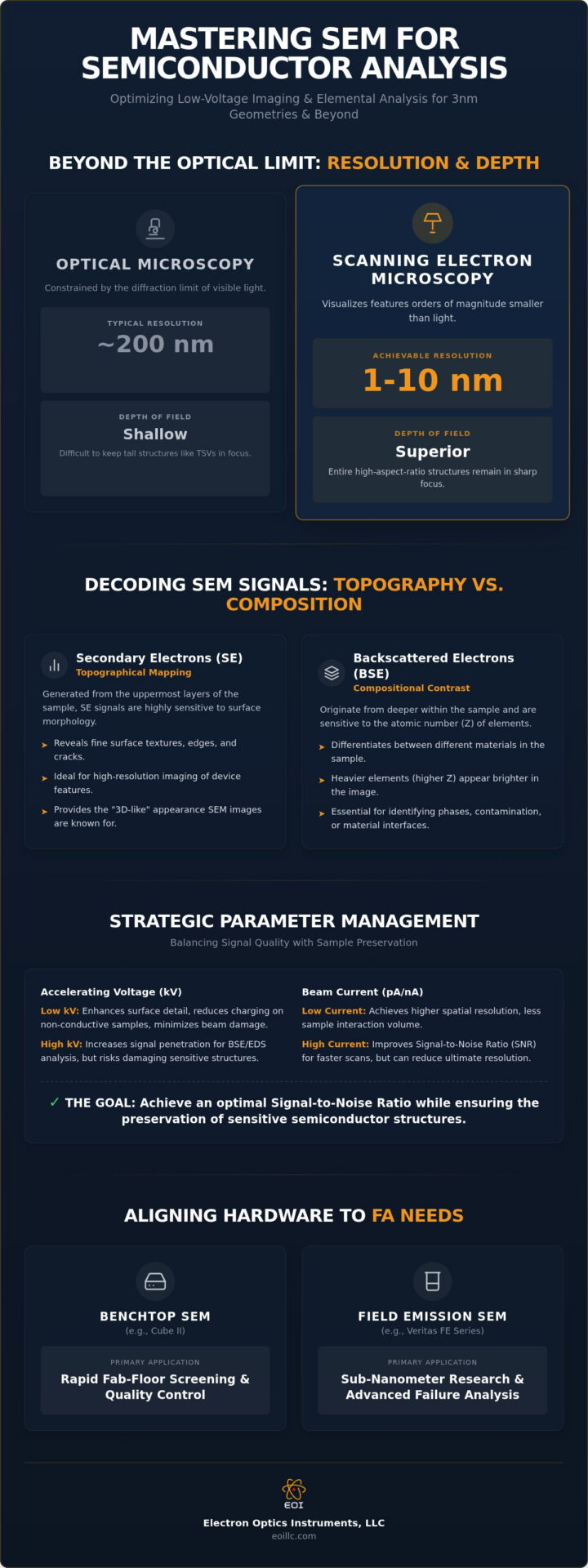
Optical systems are fundamentally constrained by the diffraction limit of visible light, typically capped at approximately 200nm. In contrast, a modern Scanning Electron Microscope (SEM) achieves nanometer-scale resolution, allowing engineers to visualize features that are orders of magnitude smaller than the wavelength of light. This capability is vital for inspecting high-aspect-ratio structures, such as Through-Silicon Vias (TSVs) and deep trenches in 3D NAND. The superior depth of field provided by electron optics ensures that both the top surface and the bottom of these deep features remain in sharp focus simultaneously, a feat that’s impossible for traditional lenses. The interaction volume represents the teardrop-shaped region within the semiconductor substrate where incident electrons undergo elastic and inelastic scattering, directly influencing the spatial resolution and depth of the resulting analytical data.
Identifying Critical Failure Modes
Isolating root causes in failed components requires the ability to visualize microscopic cracks, interfacial delamination, and the subtle onset of electromigration within metallic interconnects. As 3D IC structures become more prevalent, cross-sectional analysis using SEM becomes indispensable for verifying the integrity of vertical interconnects and the bonding between stacked dies. These advanced workflows rely on the sem scanning electron microscope fundamentals of signal detection to differentiate between material phases and structural anomalies. By leveraging these principles, manufacturers can bridge the gap between initial defect detection and long-term reliability enhancements. It’s this synergy between hardware precision and analytical expertise that maintains the industry’s trajectory toward smaller, more powerful electronic systems.
Contrast Mechanisms: SE vs. BSE in Device Inspection
The efficacy of sem for semiconductor analysis is fundamentally predicated on the sophisticated interpretation of distinct electron-sample interactions. As the primary beam scans the specimen, it generates various signals that reveal topographical and compositional data. Understanding the nuances between Secondary Electrons (SE) and Backscattered Electrons (BSE) allows failure analysis engineers to isolate specific anomalies within the intricate layers of a device. This differentiation is essential for maintaining the meticulous standards required in modern industrial sectors.
Topographical Mapping with Secondary Electrons
Secondary electrons originate from the uppermost layers of the sample, typically within the first few nanometers of the surface. This shallow escape depth makes SE imaging exceptionally sensitive to surface morphology, which is critical for identifying gate-level defects and structural irregularities. Standard Everhart-Thornley detectors provide excellent topographical contrast by capturing low-energy electrons from various angles, whereas In-lens detectors prioritize high-resolution, line-of-sight imaging. These tools are vital for improving SEM measurement accuracy in modern chip manufacturing. By utilizing low-voltage SE imaging, operators can visualize sensitive photoresists without causing beam-induced damage or excessive charging. This technique enhances edge contrast, making it easier to pinpoint microscopic fractures or delamination in complex circuitry.
Compositional Analysis via Backscattered Electrons
Backscattered electrons are high-energy electrons that are reflected back after elastic collisions with the sample’s atomic nuclei. The intensity of the BSE signal is directly proportional to the atomic number (Z) of the target material, a phenomenon known as Z-contrast. This mechanism is indispensable for identifying heavy metal contaminants, such as tungsten or copper residues, which appear significantly brighter than the surrounding silicon or dielectric matrices. Mapping these material density variations across a wafer ensures that alloy inclusions in interconnects are identified before they lead to catastrophic failure. For those seeking deeper insights into these methodologies, exploring advanced sem techniques can provide the technical foundation for high-resolution BSE mapping.
Optimizing the detector geometry is equally important for achieving directional contrast, especially when inspecting multi-layered architectures with high-aspect-ratio features. Mitigating the effects of charging on non-conductive dielectrics remains a primary concern; however, strategic parameter management and the use of specialized detectors can neutralize these artifacts. If your facility requires high-performance hardware to implement these workflows, exploring our range of Veritas FE SEM systems can provide the necessary precision for advanced device inspection. Managing these contrast mechanisms effectively ensures that every layer of the device is scrutinized with technical authority and visionary precision.
Integrated Analytical Workflows: EDS and Elemental Mapping
In the high-precision world of semiconductor fabrication, high-resolution imaging alone is often insufficient to identify the root cause of a defect. By integrating Energy Dispersive Spectroscopy (EDS) into the workflow, sem for semiconductor analysis becomes a comprehensive diagnostic platform capable of correlating morphology with chemical composition. When the electron beam strikes the sample, it displaces inner-shell electrons, prompting an outer-shell electron to fill the vacancy and release energy as a characteristic X-ray. These X-rays are unique to each element, providing a non-destructive method for precise elemental identification within the device architecture. A systematic review of SEM for semiconductor manufacturing underscores how these integrated analytical approaches are essential for maintaining yield in an increasingly complex production environment.
The choice between line scans and area mapping is a strategic decision based on the specific failure mode under investigation. Line scans provide a high-resolution profile of elemental distribution across a specific interface, which is ideal for analyzing diffusion barriers or gate dielectric stacks. Area mapping offers a spatial overview of heterogeneous inclusions, allowing engineers to visualize the distribution of contaminants across a larger field of view. To achieve quantitative accuracy in failure analysis, operators must carefully manage the take-off angle and beam current. These parameters ensure that the X-ray signal is strong enough for statistical significance without inducing beam damage in sensitive low-k dielectrics or photoresists.
Characterizing Contaminants and Inclusions
Cleanroom environments are designed to minimize risk, yet sub-micron particles remain a persistent threat to device reliability. EDS enables the rapid identification of foreign materials, distinguishing between organic residues and metallic particles derived from fabrication equipment. By mapping elemental gradients, engineers can also verify the consistency of dopant distributions and the integrity of thin-film barriers. Optimizing EDS settings for high-throughput inspection allows facilities to maintain a rigorous quality control cadence without creating a bottleneck in the analytical lab.
Advanced Analytical Integration
While EDS is the standard for most applications, high-purity layers may require Wavelength Dispersive Spectroscopy (WDS) for trace element detection. Combining these elemental maps with high-resolution secondary electron images creates a comprehensive failure analysis report that bridges the gap between physical structure and chemical reality. Adhering to established protocols for sem operation is fundamental to ensuring that these analytical results are both accurate and reproducible across different production nodes. This synergy between imaging and spectroscopy ensures that every defect is not just seen, but fully understood.
Strategic Parameter Management for Semiconductor Structures
Precision in sem for semiconductor analysis isn’t merely a result of hardware capability; it’s a product of meticulous parameter calibration tailored to the specific architecture of the device. Engineers must navigate a complex multi-dimensional space where accelerating voltage, beam current, and working distance interact to define the limits of detection. In the pursuit of sub-nanometer resolution, the accelerating voltage (kV) acts as the primary lever for controlling beam penetration. While higher voltages are necessary for imaging through thick passivation layers, they often generate an interaction volume that’s too large for surface-sensitive defect isolation. Strategic management requires a deliberate reduction in kV to localize the signal to the uppermost gate structures and interconnects.
Working distance (WD) and scan speed further refine this analytical process. A shorter WD typically enhances resolution by reducing the focal length, though it concurrently limits the depth of field, which can be problematic when inspecting high-aspect-ratio trenches. Scan speed must be adjusted to mitigate the effects of charging on non-conductive layers; slower speeds improve the signal-to-noise ratio but increase the dwell time, potentially leading to beam-induced artifacts in high-density memory arrays. Finding the equilibrium between these settings ensures that the resulting data is both high-fidelity and representative of the true physical state of the component.
Low-Voltage Imaging for Fragile Dielectrics
Modern failure analysis nodes increasingly favor imaging at levels below 5kV to prevent irreversible damage to sensitive low-k dielectrics and ultra-thin photoresists. High-energy electrons can cause localized heating or bond breaking, which alters the very structure you’re attempting to characterize. Maintaining nanometer-scale resolution at these low voltages requires advanced field emission (FE) sources that provide high brightness and a narrow energy spread. The aperture size directly dictates the beam convergence angle, which influences the depth of focus and the final resolution of the electron probe. By leveraging these low-voltage techniques, labs can achieve the clarity needed for 3nm node inspection without compromising the sample’s structural integrity.
Balancing Resolution with Equipment Longevity
Operational excellence in a high-throughput fab environment requires an understanding of how imaging parameters impact hardware health. Utilizing high-current modes to overcome noise might seem efficient, but it significantly accelerates filament degradation and necessitates more frequent sem maintenance cycles. Meticulous attention to stigmation and alignment is far more effective for preserving imaging throughput than simply increasing the beam current. Regular preventative maintenance ensures that the vacuum system and electron optics remain within the tight tolerances required for high-precision semiconductor work. To maintain this level of precision in your own facility, it’s essential to invest in high-performance semiconductor inspection systems that are engineered for both accuracy and long-term reliability.
Hardware Selection: Mapping Benchtop and FE-SEM to FA Needs
Selecting the appropriate platform for sem for semiconductor analysis requires a strategic alignment between the physical requirements of the specific production node and the operational throughput of the facility. This decision isn’t merely about choosing the most powerful tool in isolation; rather, it involves a calculated trade-off between absolute spatial resolution and logistical agility. For many industrial partners, the challenge lies in balancing the immediate needs of the fab floor with the long-term research goals of the failure analysis laboratory. A visionary approach to hardware selection considers both the immediate defect isolation requirements and the future scalability of the manufacturing process.
The Efficiency of Benchtop SEM in Fab Environments
For routine fab-floor inspection and the rapid screening of macro-defects, the Cube II Benchtop SEM provides a highly efficient and cost-effective solution. It’s often the superior choice for high-throughput screening where the goal is to identify pass/fail criteria in real-time. By lowering the barrier to entry for advanced topographical imaging, the Cube II allows engineers to perform critical inspections directly at the point of production, which prevents defective wafers from progressing further in the manufacturing chain. For those evaluating the performance metrics of these compact systems against traditional floor-standing models, our desktop sem pillar provides comprehensive comparative data to guide your integration strategy.
Advanced Characterization with Veritas FE Systems
As the semiconductor industry pushes toward next-generation Gate-All-Around (GAA) nodes, the demand for sub-nanometer resolution becomes a non-negotiable requirement. The Veritas FE Series represents the pinnacle of high-resolution semiconductor characterization, utilizing field emission sources to resolve the most minute structural anomalies that would be invisible to lesser systems. These platforms feature integrated EDS and analytical suites designed for the most demanding failure analysis challenges. This level of precision is essential for isolating root causes in complex 3D architectures where the margin for error is measured in atoms, ensuring that your quality control remains rigorous as geometries shrink.
Maximizing the return on investment for these sophisticated systems involves more than just hardware acquisition; it requires a commitment to professional technical training and full-service support to bridge the skills gap in modern FA. For facilities looking to expand their analytical capacity while managing capital expenditure, refurbished SEM units offer a reliable and cost-effective alternative. This strategic selection of hardware, combined with EOI’s 30 plus years of electron optics experience, ensures that your laboratory is equipped to meet the rigorous standards of 2026 and beyond. Contact EOI for a consultation on the ideal SEM hardware for your semiconductor lab.
Advancing Semiconductor Reliability Through Precision Electron Optics
The evolution of integrated circuits toward sub-3nm nodes demands an analytical framework that transcends mere visualization. Mastering sem for semiconductor analysis requires a meticulous integration of low-voltage imaging parameters and high-fidelity elemental mapping to ensure that structural anomalies are identified without compromising the integrity of sensitive dielectrics. By strategically aligning hardware capabilities, such as the sub-nanometer precision of the Veritas FE series or the rapid screening efficiency of the Cube II, laboratories can maintain the technical authority required to navigate the complexities of 2026 failure analysis nodes.
EOI brings over 30 years of electron optics experience to your facility, serving as the sole US distributor for EmCraft and providing comprehensive service support for all major SEM brands. This deep industry expertise ensures that your quality control processes are as rigorous as the technologies they scrutinize. Discover EOI’s High-Performance SEM Solutions for Semiconductor Labs to elevate your analytical throughput and ensure the long-term reliability of your manufacturing workflows. The future of semiconductor innovation is built upon the clarity of today’s insights.
Frequently Asked Questions
What is the primary advantage of using SEM for semiconductor analysis?
The primary advantage lies in the ability to resolve features far below the 200nm diffraction limit of optical systems while maintaining a superior depth of field. This capability allows for the precise visualization of high-aspect-ratio trenches and complex 3D IC architectures that are otherwise invisible. It’s the definitive standard for identifying sub-micron anomalies in modern manufacturing nodes where topographical fidelity is paramount.
How do I choose between SE and BSE imaging for failure analysis?
You should choose Secondary Electron (SE) imaging when the objective is to map surface morphology and identify topographical defects like gate-level fractures. Backscattered Electron (BSE) imaging is preferred for identifying material composition and phase variations. Because BSE signals correlate with atomic number, they’re indispensable for spotting heavy metal contaminants or alloy inclusions within interconnect layers.
Can a benchtop SEM like the Cube II handle semiconductor defect inspection?
A benchtop SEM like the Cube II is highly effective for rapid screening and industrial quality control where floor-standing systems aren’t required. It lowers the barrier to entry for high-throughput inspection of macro-defects and routine topographical verification. While it doesn’t reach the sub-nanometer resolution of FE systems, its logistical agility makes it a vital tool for fab-floor reliability.
Why is low-voltage imaging critical for semiconductor samples?
Low-voltage imaging is critical because it minimizes beam-induced damage to sensitive semiconductor materials like low-k dielectrics and photoresists. By operating at levels below 5kV, you reduce the electron penetration depth and localized heating that can alter fragile structures. This technique is essential for maintaining the physical integrity of the sample during sem for semiconductor analysis.
How does EDS integration improve the failure analysis workflow?
EDS integration transforms high-resolution imaging into a comprehensive diagnostic platform by correlating physical structure with chemical composition. It allows for the rapid identification of foreign particles and the mapping of elemental gradients across dopant layers. This synergy is fundamental for isolating the root causes of failure in complex, multi-layered devices without relying on separate analytical silos.
What are the common causes of image artifacts in semiconductor SEM?
Common artifacts in semiconductor imaging often stem from surface charging on non-conductive dielectric layers or hydrocarbon contamination from previous processing steps. These issues lead to beam deflection or image blurring that obscures critical details. Managing scan speeds and implementing proper vacuum protocols are necessary steps to mitigate these artifacts and ensure the acquisition of high-fidelity data.
How often should an SEM used for semiconductor analysis undergo maintenance?
Most systems used in high-throughput semiconductor environments should undergo professional preventative maintenance every six to twelve months to ensure operational stability. Regular maintenance visits focus on vacuum integrity and electron optics alignment to preserve imaging throughput. Frequent usage of high-current modes often necessitates more regular filament replacements to prevent unexpected downtime during critical inspection cycles.
Is a field emission (FE) source necessary for semiconductor research?
A field emission (FE) source is necessary for advanced research and the inspection of next-generation gate-all-around (GAA) nodes. FE sources provide the high brightness and narrow energy spread required to maintain resolution at the low voltages needed for sem for semiconductor analysis. For facilities contending with sub-10nm geometries, the Veritas FE Series offers the sub-nanometer precision required for definitive characterization.