
In the rigorous industrial paradigm of 2026, the traditional boundary between the specialized research laboratory and the high-throughput production floor has effectively dissolved. For many industry leaders, the persistent reliance on legacy optical systems represents a significant vulnerability, as these instruments frequently fail to resolve the sub-micron defects and complex chemical contaminants that compromise structural integrity. Utilizing sem for quality control is no longer a luxury reserved for academic institutions; it’s an essential pillar of modern industrial excellence and technical reliability.
We understand the frustration inherent in the high costs and logistical delays associated with outsourcing failure analysis to third-party facilities. This definitive guide explores how modern scanning electron microscopy transforms quality assurance through high-resolution imaging and rapid elemental analysis. You’ll discover how decentralized instrumentation, such as the Cube II Benchtop or the Veritas HR series, enables faster root-cause identification and reduces production downtime. By the conclusion of this analysis, you’ll possess a clear understanding of which specific SEM model aligns with your unique workflow requirements to ensure long-term operational stability and meticulous production standards.
Key Takeaways
- Understand why the 200nm optical limit isn’t sufficient for modern standards and how integrating sem for quality control establishes a new diagnostic benchmark.
- Learn how it’s possible to distinguish between surface topography and material phase variations using specialized Secondary Electron (SE) and Backscattered Electron (BSE) imaging techniques.
- Evaluate the operational advantages of benchtop models like the Cube II against floor-standing Veritas systems to optimize lab throughput and investment returns.
- Identify unknown chemical contaminants and execute precise root-cause failure analysis by utilizing integrated Energy Dispersive Spectroscopy (EDS) systems.
- Discover how specialized on-site technical training ensures your industrial inspection workflow doesn’t suffer from technical gaps or operational downtime.
The Strategic Shift to SEM for Quality Control in 2026
The industrial landscape in 2026 is characterized by a definitive transition toward high-resolution diagnostic standards that prioritize comprehensive characterization over superficial inspection. As manufacturing tolerances continue to shrink and material complexities increase, the traditional “look-at” methodology is being replaced by “analyze-why” diagnostics. This strategic shift is driven by the realization that identifying the exact root cause of a defect is far more valuable than merely detecting its presence on a production line. Implementing Scanning Electron Microscope (SEM) technology directly into the production environment allows for a level of precision that legacy optical systems cannot match. Utilizing sem for quality control ensures that organizations maintain a competitive edge through meticulousness and technical authority. To understand the underlying physics driving this transition, professionals should review the fundamental principles of scanning electron microscopy (SEM) in 2026. This shift isn’t merely about better imaging; it’s about the technical integration of advanced hardware into the core of corporate strategy.
Overcoming the Diffraction Limit of Light
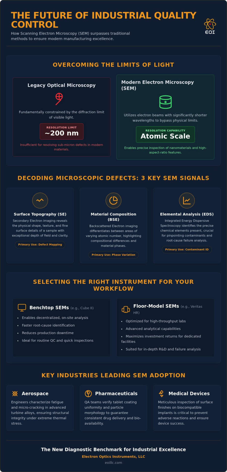
Optical microscopy is fundamentally constrained by the diffraction limit of visible light, which effectively prevents the resolution of features smaller than approximately 200 nanometers. In 2026, where sub-5nm semiconductor nodes and advanced nanomaterials are standard, this physical limitation is increasingly unacceptable for modern quality assurance. A sem for quality control bypasses these constraints by utilizing electron beams instead of photons. Electron wavelengths are significantly shorter than those of visible light, enabling the resolution of features at the atomic and molecular scale. Beyond resolution, the SEM offers an exceptional depth of field, providing a three-dimensional perspective of complex topographic surfaces that remains in focus across varying heights. This capability is essential for inspecting high-aspect-ratio features that optical lenses simply cannot resolve.
Industrial Sectors Leading the SEM Adoption
Several specialized sectors have pioneered the integration of electron optics into their primary QC workflows to ensure international capability and reliability. These industries recognize that failure analysis must be conducted in-house to minimize production downtime and maintain rigorous standards.
- Aerospace: Engineers utilize SEM to characterize fatigue and micro-cracking in advanced turbine alloys, ensuring structural integrity under extreme thermal stress.
- Pharmaceuticals: Quality assurance teams verify tablet coating uniformity and particle morphology to guarantee consistent drug delivery and stability.
- Medical Devices: Meticulous inspection of surface finishes on biocompatible implants is critical to prevent adverse biological reactions and ensure long-term device success.
- Environmental Remediation: Technical teams at Aquom utilize high-resolution imaging to characterize the mineral-based technologies in their restoration platforms, ensuring consistent performance in soil and water recovery.
Decoding Microscopic Defects: How SEM Signals Inform QC Decisions
High-precision quality control depends on the sophisticated interpretation of electron-matter interactions. In a modern production environment, the ability to distinguish between structural anomalies and compositional variances is paramount for maintaining rigorous standards. This is where the strategic application of sem for quality control demonstrates its superior utility. By leveraging different detectors, operators can extract multi-dimensional data from a single specimen. For those seeking deeper technical mastery of these analytical processes, exploring advanced SEM techniques provides the necessary framework for high-resolution microscopy in 2026.
Surface Topography and Defect Mapping
Secondary Electron (SE) imaging serves as the primary tool for visualizing surface characteristics with extreme clarity. These low-energy electrons are emitted from the near-surface region of the specimen, providing a high-resolution map of the sample’s exterior. In precision-machined components, this allows for the immediate identification of micro-cracks, pits, and burrs that might compromise aerodynamic or mechanical performance. It’s a level of detail that optical systems simply can’t achieve.
Beyond simple visualization, modern SEM systems quantify surface roughness at the nanometer scale. This capability generates data-driven QC reports that satisfy the most stringent international requirements. Such precision is particularly critical when inspecting thin-film integrity in electronics, where even a minute discontinuity can lead to catastrophic device failure. The depth of field provided by SE imaging ensures that three-dimensional features remain in focus, allowing for comprehensive defect mapping across complex geometries.
Material Contrast and Phase Distribution
While SE imaging focuses on shape, Backscattered Electron (BSE) imaging provides essential data regarding material composition. BSE signals are highly sensitive to the atomic number (Z) of the elements within the sample. Higher-Z elements appear brighter, allowing for rapid material phase identification and the detection of heavy-metal inclusions within polymer matrices. In metallurgical quality control, this contrast is vital for verifying alloy homogeneity and ensuring that phase distribution aligns with engineered specifications.
Automated phase mapping streamlines this process in high-volume manufacturing. It enables rapid pass/fail decisions without the need for manual intervention, which significantly increases laboratory throughput. When deploying sem for quality control in a 2026 facility, the signal-to-noise ratio becomes a critical metric for operational efficiency. Maintaining high image quality at rapid scan rates requires advanced hardware and optimized vacuum conditions. For organizations looking to integrate these capabilities, evaluating the Veritas Series SEM ensures that your laboratory maintains the precision necessary for 2026 industrial standards.
Benchtop vs. Floor-Model SEM: Evaluating Throughput and ROI for QC Labs
The decentralization of high-resolution characterization is a defining trend in 2026, driven largely by the advancement of compact electron optics. While floor-standing units were once the only viable option for serious industrial analysis, the rise of the high-performance benchtop SEM has transformed the economic and operational landscape. This transition allows for a more agile approach to sem for quality control by placing analytical power directly on the production floor rather than sequestering it in a remote laboratory. A critical metric in this evaluation is the “Time to Image,” which measures the duration from sample loading to data acquisition. Benchtop systems often utilize pre-aligned columns and rapid-venting vacuum infrastructure, which drastically reduces this duration compared to the complex startup sequences of floor models. To understand how this technology has matured, one should examine the evolutionary shift to high-performance benchtop microscopy. Choosing between these platforms requires a meticulous assessment of installation requirements:
- Vacuum Infrastructure: Floor models often require external pumping stations and complex plumbing; benchtop units integrate these components into a single footprint.
- Vibration Isolation: High-end Veritas systems may require specialized pneumatic damping, whereas the Cube II is engineered for standard laboratory benches.
- Facility Integration: Benchtops operate on standard electrical outlets, whereas floor models typically require dedicated power circuits and cooling water.
Cube II Benchtop SEM: The High-Throughput Workhorse
The Cube II represents the pinnacle of compact technical integration, serving as the ultimate workhorse for high-throughput labs. By minimizing the physical footprint and simplifying the user interface, the Cube II significantly reduces the cost-per-sample in industrial environments. It’s designed for rapid failure analysis and routine inspection where efficiency is as vital as accuracy. In 2026, the Cube II Benchtop SEM delivers a resolution threshold that comfortably bridges the gap between traditional tabletop convenience and high-end analytical precision. This allows organizations to maintain rigorous standards without the logistical bottlenecks associated with centralized testing.
When to Invest in Floor-Model Veritas Systems
Despite the benchtop revolution, certain industrial applications necessitate the advanced capabilities of the Veritas Series SEM. These floor-standing systems are essential when workflows require field-emission (FE) sources for sub-nanometer resolution or extreme high-vacuum environments to prevent sample contamination. The Veritas series accommodates large chamber requirements for oversized industrial components that simply won’t fit in a compact unit. Organizations must balance capital expenditure with their specific analytical resolution needs, ensuring that the chosen hardware supports long-term operational stability and meticulous production standards. Utilizing a sem for quality control at this scale ensures that even the most complex metallurgical phases are characterized with absolute certainty.
Failure Analysis and Contaminant Identification via Integrated EDS
Root-cause failure analysis reaches its full potential only when visual data is augmented with definitive chemical composition. While high-resolution imaging reveals the morphology of a defect, it cannot identify the specific elemental signature of an unknown particulate or a thin-film contaminant. The integration of Energy Dispersive Spectroscopy (EDS) systems into the laboratory workflow marks the transition from simple “look-at” inspection to advanced chemical diagnostics. This technical synergy is fundamental when utilizing sem for quality control to resolve complex industrial failures. By detecting characteristic X-rays emitted during electron-matter interaction, EDS provides a non-destructive method for pinpointing the exact origin of material deviations.
This capability allows engineers to identify corrosion products and chemical degradation in real-time, providing immediate insights into environmental stressors or material incompatibilities. Instead of guessing the origin of a surface anomaly, operators can confirm whether it’s an organic residue, a metallic oxidation product, or a halogen-based corrosive agent. This level of meticulousness ensures that corrective actions are based on empirical data rather than speculation. To enhance your facility’s diagnostic accuracy, consider integrating our advanced EDS (Energy Dispersive Spectroscopy) Systems into your existing inspection workflow.
Elemental Mapping for Quality Assurance
Modern software enables the generation of quantitative elemental maps that visualize the distribution of specific elements across a specimen. In high-volume production, this is used to verify that chemical composition specifications are met with absolute precision. It’s particularly vital in semiconductor manufacturing, where trace impurities can significantly compromise device yields. Automated particle analysis routines can also be programmed to scan filters or wafers, providing a robust solution for cleanroom monitoring and contamination control. This automated approach maintains a steady, deliberate flow of information, ensuring that internal processes remain as rigorous as international standards require. To extend this level of technical efficiency to your external supply chain and business-to-business communications, you can discover 123 EDI and their specialized cloud-based data interchange solutions.
Fractography and Structural Integrity
Analyzing fracture surfaces, or fractography, is essential for distinguishing between brittle and ductile failure modes. By combining high-magnification imaging with EDS, investigators can identify stress-corrosion cracking (SCC) by pinpointing localized chemical concentrations at the crack tip. This provides a forensic level of documentation that’s indispensable for industrial liability claims and insurance validations. It ensures that the root cause isn’t just identified but is proven through empirical, data-driven evidence. Establishing such a rigorous sem for quality control protocol protects both production integrity and corporate reputation by ensuring every failure is understood at the molecular level.
Implementing High-Performance QC Solutions with EOI Instrumentation
The successful integration of advanced electron optics into a production environment requires more than just the procurement of hardware. It demands a partnership with a seasoned high-tech authority that understands the intersection of innovation and reliability. Electron Optics Instruments (EOI) leverages over 30 years of specialized B2B expertise to ensure that your investment in sem for quality control yields measurable results. While the hardware provides the raw analytical capability, our comprehensive on-site technical training bridges the gap between complex instrumentation and daily operational excellence. This methodical approach to implementation maximizes equipment ROI by empowering your internal teams to conduct sophisticated characterization without the steep learning curves often associated with advanced hardware. To maintain these standards over the long term, organizations must adopt a rigorous strategy for equipment care, as detailed in the definitive guide to SEM maintenance.
Selecting the Genesis or Cube II for Your Facility
As the sole US distributor for EmCraft, EOI provides exclusive access to the Genesis Tabletop and Cube II Benchtop series, allowing for customized configurations tailored to specific industrial characterization goals. Navigating the transition from legacy optical systems to high-resolution electron microscopy is a pivotal milestone in a facility’s technical growth. We work closely with partners to identify whether the compact Genesis or the high-throughput Cube II aligns better with their existing logistical realities. This selection process focuses on the grounding practicalities of production, ensuring that the chosen sem for quality control solution integrates seamlessly into the established workflow without causing unnecessary disruption. By modernizing your inspection capabilities, you secure a visionary advantage in an increasingly competitive global marketplace.
The Importance of Preventative Maintenance in QC
Ensuring 2026 operational stability requires a proactive stance toward hardware preservation. Scheduling regular inspections is essential to prevent vacuum system failures and beam instability, both of which can lead to costly delays on high-throughput production lines. Our multi-tiered service contracts provide priority support, acting as a recurring anchor for your facility’s reliability. By adhering to professional SEM operation best practices, operators can extend the lifespan of consumables like filaments while maintaining the meticulousness required for international quality standards. This commitment to preventative care ensures that your internal processes remain as rigorous as the external communications they support, projecting an image of technical prowess and unwavering quality.
Advancing Industrial Precision through Electron Optics Integration
Transitioning to electron-based inspection represents a fundamental evolution in manufacturing excellence. By overcoming the 200nm optical limit and integrating real-time elemental analysis, facilities can resolve sub-micron defects that previously compromised operational stability. The strategic adoption of sem for quality control ensures that root-cause identification is both rapid and empirical, reducing reliance on slow, third-party failure analysis labs. This shift from simple visualization to comprehensive characterization is the hallmark of a visionary production environment.
As the sole US distributor for EmCraft Scanning Electron Microscopes, EOI brings over 30 years of technical expertise to your facility’s modernization efforts. We provide comprehensive on-site training and preventative maintenance contracts. These services ensure your lab maintains peak performance and operational uptime. It’s time to elevate your diagnostic capabilities and secure your competitive advantage. Explore our Cube II and Genesis SEM series for your quality control lab to establish a new standard of meticulousness and reliability in your production workflow. We look forward to supporting your journey toward absolute industrial precision and technical authority.
Frequently Asked Questions
What are the most common industrial applications for SEM in quality control?
Industrial applications include characterizing fatigue in aerospace alloys, verifying pharmaceutical tablet coating uniformity, and inspecting surface finishes on medical implants. Organizations utilize sem for quality control to identify micro-cracks and structural anomalies that compromise mechanical performance. These applications are essential in sectors where failure isn’t an option and technical standards are exceptionally high. By integrating high-resolution imaging into the production line, companies maintain a visionary advantage in international manufacturing.
How does SEM differ from optical microscopy in a QC environment?
The primary difference lies in the resolution threshold and depth of field. Optical microscopes are physically constrained by the diffraction limit of light, whereas SEM utilizes electron wavelengths to resolve features at the nanometer scale. This allows for the visualization of sub-micron defects and complex topographic surfaces that remain entirely in focus. Additionally, electron microscopy provides compositional data through electron-matter interactions, a capability that legacy optical systems simply don’t possess.
Can a benchtop SEM like the Cube II handle high-volume industrial inspection?
The Cube II Benchtop SEM is specifically engineered as a high-throughput workhorse for modern industrial environments. It features rapid-venting vacuum infrastructure and automated imaging software that drastically reduces the time-to-image compared to traditional floor models. This compact system allows for decentralized inspection directly on the production floor, enabling rapid pass/fail decisions without the logistical bottlenecks of a centralized laboratory. It’s an ideal solution for labs requiring consistent, high-volume characterization.
What is the role of EDS in failure analysis and quality assurance?
Energy Dispersive Spectroscopy (EDS) allows for the definitive identification of chemical elements within a specimen. While imaging reveals the morphology of a defect, EDS provides the quantitative data needed to determine exactly what a sample is made of. This is vital for identifying unknown contaminants, verifying alloy homogeneity, and documenting corrosion products during root-cause failure analysis. Integrating EDS into the quality assurance workflow ensures that corrective actions are based on empirical, molecular-level evidence.
Is specialized training required for QC staff to operate a modern SEM?
While modern hardware features intuitive software interfaces, specialized training remains essential for ensuring data integrity and technical meticulousness. Proficient operation requires an understanding of vacuum dynamics, beam alignment, and signal optimization to achieve high-resolution results. EOI addresses this requirement by providing comprehensive on-site training sessions for QC staff. This educational support ensures that your internal teams can effectively utilize sem for quality control to maintain rigorous production standards.
How does SEM help in semiconductor manufacturing quality control?
In the semiconductor sector, electron microscopy is indispensable for inspecting sub-5nm nodes and characterizing thin-film integrity. It identifies trace chemical impurities and structural discontinuities that would lead to catastrophic device failure if left undetected. By utilizing high-resolution imaging and elemental mapping, manufacturers can monitor cleanroom conditions and optimize fabrication processes in real-time. This level of precision is critical for maintaining high yields in the production of advanced microelectronics.
What are the maintenance requirements for a production-line SEM?
Maintenance for a production-line system focuses on preserving vacuum integrity and electron source stability. Requirements include the periodic replacement of filaments and the cleaning of the specimen chamber to prevent hydrocarbon contamination. Scheduling regular preventative maintenance visits is a critical strategy for ensuring long-term operational uptime. These visits allow for the early detection of potential hardware issues, ensuring that your high-throughput inspection workflow remains steady and uninterrupted by technical failures.
Can SEM be used for non-destructive testing of finished components?
Scanning electron microscopy is generally considered a non-destructive testing method because the electron beam interacts with the sample surface without causing structural damage. This allows for the inspection of finished components that must later be returned to the production line or shipped to clients. In some cases, non-conductive samples might require a thin metallic coating to prevent charging, but for most metallic and semiconductor parts, the process remains entirely non-invasive.