
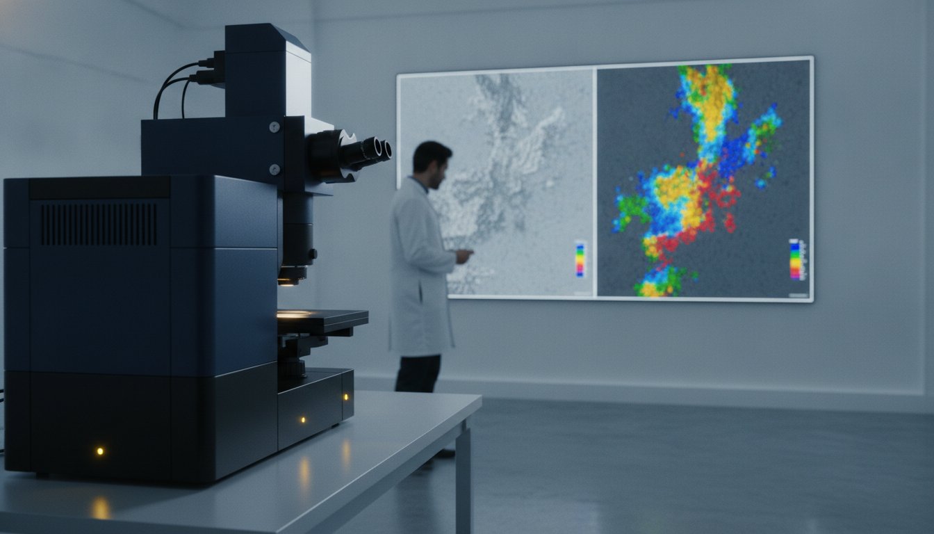
Could the precision of your microstructural analysis be compromised not by the hardware itself, but by a fundamental misalignment between electron-sample interactions and your chosen imaging parameters? While the microscopy market is projected to reach USD 6.24 billion by 2026, the efficacy of this investment for diverse benchtop sem applications relies entirely on the operator’s ability to navigate complex signal nuances. You likely recognize that achieving sub-5nm resolution requires more than just high-end equipment. It’s often a source of professional frustration when charging artifacts obscure non-conductive samples or when it becomes difficult to distinguish between topographical features and material density variations.
This comprehensive guide provides the technical framework to master core and advanced scanning electron microscopy imaging techniques, ensuring you can optimize resolution, contrast, and analytical depth for demanding industrial environments. By refining your methodology, you’ll gain a clear understanding of the interplay between Secondary Electron (SE) and Backscattered Electron (BSE) signals. We will examine how to optimize accelerating voltage and working distance for specific results, while identifying exactly when to utilize EDS integration for superior analytical clarity. This methodical overview ensures your laboratory transitions from basic observation to high-fidelity characterization using systems such as the Cube II or Veritas series.
Key Takeaways
- Learn to differentiate between Secondary Electron (SE) and Backscattered Electron (BSE) signals to interpret surface topography versus material composition with absolute precision.
- Master advanced topographic analysis by utilizing Everhart-Thornley and In-Lens detectors to capture ultra-fine nanostructures previously limited to large-scale floor systems.
- Optimize resolution and contrast for diverse benchtop sem applications by strategically balancing accelerating voltage and working distance based on specific sample density.
- Implement compositional mapping through segmented BSE detectors and directional shadowing to visualize elemental distribution and material density on complex surfaces.
- Leverage high-performance hardware like the Cube II and Veritas Series to achieve superior spatial resolution and automated analytical depth within a compact laboratory footprint.
The Fundamentals of Signal Generation: Secondary vs. Backscattered Electrons
The efficacy of modern microstructural characterization relies on the strategic manipulation of the interaction volume. When the primary electron beam of a Scanning Electron Microscope (SEM) strikes a specimen, it penetrates the surface to form a discrete, three-dimensional region of excitation. The geometry of this volume is a function of the beam’s energy and the specimen’s material properties. For those navigating diverse benchtop sem applications, understanding this penetration is crucial. It dictates whether the resulting data reflects surface-level morphology or deeper compositional truths. The choice between signal types isn’t merely a preference; it’s a calculated decision that defines the analytical depth of the microscopy session.
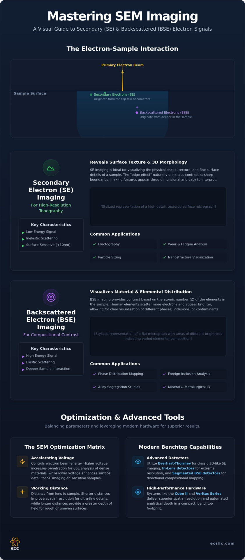
Secondary electrons and backscattered electrons represent the two pillars of signal generation. Secondary electrons (SE) are the result of inelastic scattering, where energy is transferred to the sample’s electrons, causing their ejection. Due to their low kinetic energy, only those generated within the first few nanometers of the surface can escape. In contrast, backscattered electrons (BSE) are beam electrons that have been elastically deflected by the nuclei of the sample atoms. These carry significantly higher energy and originate from much deeper within the interaction volume. By selecting the appropriate detector and signal, operators can transition from observing surface roughness to identifying the elemental distribution of a multi-component alloy. This fundamental distinction ensures that the imaging process is a tailored technical approach rather than a generic procedure.
Secondary Electron (SE) Imaging for Topographical Detail
Backscattered Electron (BSE) Imaging for Compositional Contrast
Backscattered electron imaging utilizes elastic scattering to provide compositional contrast based on atomic number sensitivity. Heavier elements scatter electrons more efficiently and appear brighter, enabling the rapid identification of phase distributions and foreign inclusions within a sample. This Z-contrast is essential for locating metallic particles in polymer matrices or identifying alloy segregations. Advanced systems like the Cube II and Veritas Series use segmented detectors to ensure precise material characterization across complex, multi-phase specimens.
Mastering Topographic Analysis: Advanced SE Imaging Techniques
High-resolution surface capture in modern benchtop sem applications requires a meticulous understanding of detector geometry and signal collection efficiency. The Everhart-Thornley detector (ETD) remains a cornerstone for general topographic imaging, utilizing a biased grid to attract low-energy secondary electrons. This creates the classic 3D look by highlighting shadows and edges across complex textures. However, for ultra-fine nanostructures, In-Lens detectors found in high-end units like the Veritas HR provide superior spatial resolution by collecting signals directly within the electron column, minimizing chromatic aberration and maximizing signal-to-noise ratios at extreme magnifications.
Imaging non-conductive specimens, such as biological tissues or advanced polymers, often presents the challenge of electron accumulation. This charging effect manifests as bright streaks or image distortion, which can compromise data integrity and obscure fine details. While traditional methods rely on heavy metallic coatings, modern strategies favor optimizing the primary beam to achieve a state of charge equilibrium, ensuring the specimen remains stable during the scan.
Low-Voltage (Low-kV) Imaging Strategies
Operating at lower accelerating voltages, typically below 5kV, is essential for observing the true surface of sensitive materials. By reducing beam penetration, operators can capture surface-most details that would otherwise be washed out by deeper interactions within the specimen. This approach is vital for soft material characterization and ensures that delicate structures remain intact during observation. To explore more sophisticated methodologies for these sensitive samples, consult our guide on Advanced SEM Techniques. Achieving charge balance at these lower energies allows for the imaging of ceramics and polymers without the immediate need for metal sputtering, preserving the specimen’s native state.
Surface Preparation and Coating Requirements
When low-kV strategies aren’t sufficient, surface modification becomes necessary to provide a conductive path for electrons. Gold sputtering is preferred for high-resolution SE imaging due to its high secondary electron yield, whereas carbon is prioritized when Energy Dispersive Spectroscopy (EDS) analysis is required to avoid X-ray interference. Understanding the Fundamental Principles of SEM helps in selecting the correct coating thickness to balance conductivity with resolution. Excessive coating can lead to the decoration effect, where the metal layer creates its own artificial texture. The critical point where coating thickness begins to obscure real topographical data occurs when the metal layer exceeds the size of the smallest features of interest. For laboratories seeking to refine these preparation protocols, our team provides specialized technical training and support for the entire Veritas and Cube II product lines.
Compositional Mapping and Material Characterization with BSE
Backscattered electron (BSE) signals provide a critical layer of analytical depth, particularly within industrial benchtop sem applications where material identification is as vital as topographic clarity. Unlike secondary electrons that primarily reveal surface features, BSE signals originate from deeper elastic scattering events within the interaction volume. Modern systems, such as the Cube II and Veritas Series, utilize high-sensitivity, multi-segmented BSE detectors that allow for the simultaneous acquisition of topographic and compositional data. By manipulating these detector segments, operators can isolate Z-contrast, which directly correlates image brightness with the atomic number of the specimen’s constituents. Heavier elements scatter electrons more efficiently, appearing brighter than lighter elements, which facilitates rapid phase identification without the immediate need for chemical mapping.
Directional BSE imaging also enables advanced shadowing techniques. By selectively activating specific detector quadrants, one can simulate directional lighting on otherwise flat surfaces, revealing subtle height variations that might be missed in a standard SE scan. This capability is indispensable during failure analysis, where identifying crack propagation across distinct material phases requires a clear distinction between the mechanical fracture path and the underlying microstructural boundaries. This allows for a more rigorous assessment of how material fatigue interacts with specific grain structures or inclusions.
Phase Identification and Grain Boundary Analysis
Mapping multi-phase alloys and complex composite materials is a cornerstone of modern industrial quality control. Within semiconductor failure analysis workflows, BSE imaging is frequently employed to detect sub-surface inclusions that disrupt electrical continuity. In corrosive studies, the high sensitivity of the BSE signal allows researchers to distinguish between thin oxidation layers and the base metal substrate. This provides a visual representation of material degradation over time, ensuring that protective coatings meet the required engineering standards for durability and performance.
Integrating BSE with EDS for Holistic Analysis
The synergy between Z-contrast imaging and X-ray microanalysis creates a comprehensive framework for chemical verification. BSE serves as a precise visual map, guiding the operator toward specific regions of interest for targeted elemental point analysis or high-resolution mapping. This integrated approach ensures that the visual brightness observed in the BSE image is accurately validated by Energy Dispersive Spectroscopy (EDS) data. To master these foundational concepts, reviewing The Fundamental Principles of SEM is essential for optimizing your analytical workflow. By aligning visual evidence with precise chemical data, professionals can achieve a higher standard of accuracy in their benchtop sem applications, ensuring that microstructural conclusions are supported by multiple analytical vectors.
The SEM Optimization Matrix: Balancing Resolution and Contrast
Achieving peak performance in benchtop sem applications requires a rigorous management of interdependent variables within the electron column. The accelerating voltage (kV) must be calibrated precisely to the specimen’s density; higher energy provides the penetration needed for Z-contrast in metallic alloys, while lower energy preserves the surface integrity of delicate polymers. Spot size and beam current also demand careful consideration. While a smaller spot size theoretically enhances spatial resolution, it simultaneously reduces the number of electrons reaching the detector, which can lead to a degraded signal-to-noise ratio. Professional operators must navigate this trade-off to ensure that high-magnification images remain crisp and interpretable. Final lens settings and aperture selection further influence beam convergence, directly impacting the sharpness of the final micrograph.
The Working Distance (WD) Trade-off
The physical gap between the final lens and the specimen, known as the working distance, dictates both the depth of field and the ultimate spatial resolution. Implementing a short WD, typically between 5mm and 10mm, is standard for high-resolution secondary electron imaging, as it minimizes the beam’s divergence. Conversely, a longer WD is preferred when imaging samples with significant height variations, such as fractured surfaces or large particles, to maintain a consistent focus across the entire field of view. The collection efficiency of BSE detectors often peaks at specific distances depending on the system’s geometry. The sweet spot for benchtop SEM topography in industrial R&D typically resides between 10mm and 15mm, providing an optimal balance of analytical signal and focus depth.
Managing Signal-to-Noise in High-Magnification Imaging
Noise reduction is a critical factor when pushing the limits of benchtop systems at high magnifications. Operators can choose between slower scan rates, which allow more dwell time per pixel to accumulate signal, or frame averaging, which overlays multiple rapid scans to cancel out random electronic noise. Beyond internal settings, external factors such as floor vibrations and electromagnetic interference can introduce artifacts that obscure nanometer-scale features. Adhering to SEM Operation Best Practices ensures that these environmental variables are mitigated before they compromise data quality. For organizations looking to upgrade their current analytical capabilities with high-stability hardware, we recommend exploring the Veritas Series for industry-leading resolution and reliability. This methodical approach to parameter optimization ensures that every session yields the maximum possible information from the specimen.
Modern Benchtop SEM Capabilities: High-Performance Imaging in a Compact Form
The progression of electron optics has fundamentally altered the landscape of industrial characterization by neutralizing the traditional trade-offs between system size and imaging capability. While floor-model systems were once deemed the only viable path for high-end research, the Cube II Benchtop SEM delivers comparable spatial resolution within a footprint designed for modern laboratory agility. This shift toward decentralized analysis represents a significant trend in benchtop sem applications for 2026, allowing for point-of-need verification directly on production floors where immediate data is required for critical decision-making. Moving beyond the limitations of traditional light microscopy, these systems provide a superior depth of field and the analytical versatility required for complex failure analysis in specialized sectors. Maintaining this level of precision over the long term necessitates a rigorous adherence to professional SEM Maintenance and Service to preserve vacuum stability and electron source longevity.
Advanced Detectors in the Cube II and Veritas Series
The Veritas Series, including the Veritas HR and Veritas FE models, incorporates sophisticated detection hardware tailored for high-throughput industrial environments. High-sensitivity 4-quadrant BSE detectors enable instantaneous material screening by providing simultaneous Z-contrast and topographic data, which streamlines the identification of phase boundaries and foreign inclusions within composite specimens. These platforms often feature integrated EDS systems that allow for real-time chemical characterization without the need for sample transfer or complex realignment procedures. By employing automated imaging workflows, laboratories analyzing high-purity research peptides from Biomod Peptides can maintain rigorous quality control standards while significantly increasing sample throughput across multiple shifts. These capabilities ensure that even the most demanding microstructural requirements are met with consistency, providing a level of technical accuracy that was previously inaccessible to compact platforms.
Technical Training: Unlocking the Full Potential of Your SEM
Acquiring state-of-the-art hardware is only the first stage in establishing a world-class microscopy workflow. Professional on-site training is the critical variable that allows operators to fully leverage the advanced features of modern benchtop sem applications. It’s this expert-led education that minimizes the risk of data misinterpretation and equipment downtime, fostering a culture of technical meticulousness that mirrors the rigorous internal processes of global industry leaders. Customized training protocols improve laboratory ROI by ensuring that technicians can navigate the optimization matrix of kV and beam current with total confidence. For organizations seeking to integrate these high-performance systems into their existing infrastructure, Contact Electron Optics Instruments, LLC for a consultation on Cube II or Veritas SEM solutions. Our team provides the strategic insight and technical support required to achieve superior characterization outcomes.
Advancing Analytical Standards in Microstructural Characterization
The evolution of electron optics has fundamentally redefined what’s achievable within a decentralized laboratory environment. By mastering the synergy between beam energy and geometric parameters, professionals can now extract maximum analytical depth from diverse benchtop sem applications. The strategic use of advanced detectors ensures that the distinction between topography and material composition is maintained with absolute clarity. This methodical approach to imaging transforms a compact system into a powerful engine for industrial innovation and research excellence.
As the sole US distributor for EmCraft, Electron Optics Instruments, LLC brings over 30 years of technical expertise to every partnership. We provide not only industry-leading hardware but also the comprehensive on-site training and support necessary to transform complex imaging theory into practical results. Whether you’re optimizing fracture analysis or conducting multi-phase material characterization, our team ensures your equipment operates at peak precision. Contact Electron Optics Instruments, LLC to Explore the Cube II and Veritas SEM Series and discover how our specialized systems can elevate your characterization capabilities. We’re ready to help you push the boundaries of what’s possible in high-resolution microscopy.
Frequently Asked Questions
What is the difference between SE and BSE imaging techniques?
Secondary electron (SE) imaging primarily captures the topographical morphology of a specimen’s surface by detecting low-energy electrons ejected from the first few nanometers. Backscattered electron (BSE) imaging utilizes high-energy electrons reflected from deeper within the interaction volume to provide compositional contrast. This Z-contrast allows for the immediate identification of different material phases based on atomic number, where heavier elements appear brighter than lighter ones, facilitating rapid microstructural screening across complex industrial samples.
When should I use low accelerating voltage (low kV) for SEM imaging?
Low accelerating voltage, typically below 5kV, is essential when imaging non-conductive, heat-sensitive, or delicate specimens such as polymers and biological tissues. This technique reduces the electron beam’s penetration depth, which enhances surface-most details and mitigates the accumulation of static charge. By achieving a state of charge equilibrium, operators can often bypass the need for conductive coatings, preserving the native state of the specimen for more accurate characterization in benchtop sem applications.
How does working distance affect SEM image quality?
Working distance (WD) represents the vertical gap between the final pole piece and the specimen surface. A shorter WD, often between 5mm and 10mm, minimizes the beam’s divergence to achieve maximum spatial resolution for high-magnification imaging. Conversely, a longer WD increases the depth of field, which is critical for maintaining focus across highly textured or fractured surfaces. Strategic WD selection ensures a balance between ultimate clarity and the three-dimensional integrity of the final micrograph.
Do I always need to coat my samples for SEM imaging?
Conductive coating is not always a requirement in modern microscopy. While gold or carbon sputtering prevents charging on non-conductive samples, advanced benchtop sem applications often utilize low-voltage imaging or low-vacuum modes to manage electron accumulation. These strategies allow for the direct observation of ceramics, plastics, and biological materials without the risk of obscuring fine topographical features with a metallic layer, ensuring the integrity of the original specimen is maintained throughout the analysis.
What is the best SEM technique for failure analysis in electronics?
Effective electronic failure analysis requires a multi-modal approach combining BSE imaging with Energy Dispersive Spectroscopy (EDS). BSE is particularly proficient at identifying metallic inclusions, whisker growth, and solder joint fractures through Z-contrast differentiation. SE imaging provides the necessary topographical detail to map mechanical fatigue or surface contamination. Integrating these techniques within a high-performance system like the Veritas Series allows for a holistic investigation into the root causes of component degradation and manufacturing defects.
Can benchtop SEMs perform high-resolution imaging comparable to floor models?
High-performance benchtop SEMs, such as the Cube II and Veritas Series, now achieve sub-5nm spatial resolution, effectively bridging the gap that once separated them from traditional floor-standing units. While floor models remain necessary for sub-nanometer research and extremely large specimens, modern benchtop systems possess the electron optics and detector sensitivity required for the vast majority of industrial quality control and research tasks. This technological convergence offers institutional-grade precision within a significantly more accessible and compact laboratory footprint.
How does spot size influence the signal-to-noise ratio in SEM?
Spot size directly influences the trade-off between spatial resolution and signal-to-noise ratio. A smaller spot size focuses the electron beam more tightly, which is necessary for resolving nanometer-scale features, but it results in a lower beam current reaching the specimen. This reduction in signal can lead to grainier images unless scan rates are slowed significantly. Finding the optimal spot size involves balancing the need for crisp detail with the requirement for a clean, noise-free analytical signal during high-magnification sessions.
What role does Energy Dispersive Spectroscopy (EDS) play in SEM imaging?
Energy Dispersive Spectroscopy (EDS) functions as the primary tool for elemental characterization within the electron microscope. By detecting characteristic X-rays emitted from the specimen during beam interaction, EDS allows operators to map the chemical composition of specific microstructures identified during imaging. This synergy between visual Z-contrast and quantitative chemical data is vital for validating material phases, identifying unknown contaminants, and ensuring that industrial production meets stringent metallurgical or chemical standards across diverse manufacturing sectors.