
The traditional boundary between high-resolution imaging and sample integrity has effectively dissolved with the advent of 2026 microscopy standards. You likely recognize the persistent frustration of managing destructive charging on non-conductive polymers or the struggle to achieve sub-nanometer resolution without compromising delicate surface topography. These technical limitations often hinder the precise correlation of chemical composition with complex physical structures, stalling critical nanomaterial characterization. This professional guide provides the expertise necessary to master the sophisticated imaging modalities and low vacuum sem techniques that transform a standard laboratory into a high-resolution, multidimensional analytical hub. By adopting these innovations, you can perform non-destructive chemical analysis while maximizing throughput via automated workflows. We will explore the strategic integration of field-emission hardware, such as the Veritas FE SEM, alongside the latest ISO 25387:2026 protocols for determining point resolution. This analysis details how modern advancements in hardware and software synthesis are redefining the capabilities of the industrial laboratory through meticulous technical integration and visionary engineering.
Key Takeaways
- Master the transition from qualitative topographical observation to precise quantitative characterization by leveraging the high-resolution capabilities of field emission hardware.
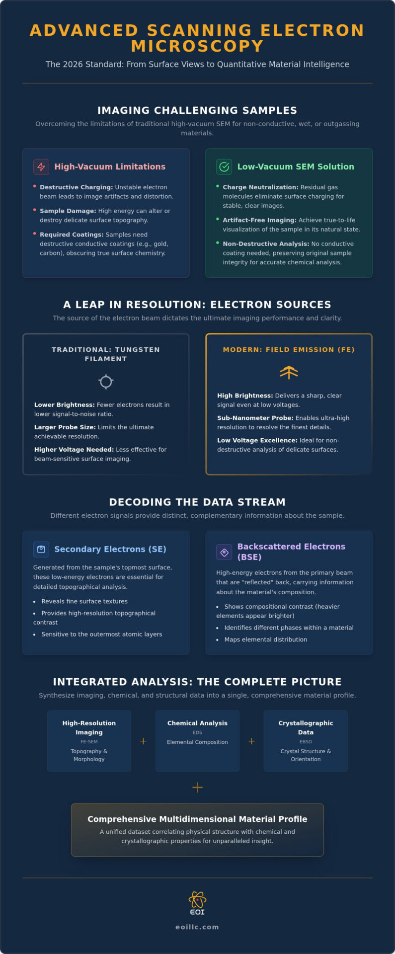
- Implement sophisticated low vacuum sem techniques to achieve artifact-free imaging of non-conductive, wet, or outgassing samples without the requirement for destructive conductive coatings.
- Integrate real-time Energy Dispersive Spectroscopy (EDS) and Electron Backscatter Diffraction (EBSD) to synthesize chemical and crystallographic data into a comprehensive multidimensional material profile.
- Evaluate the strategic importance of professional on-site technical training and rigorous preventative maintenance in maintaining the sub-nanometer resolution standards required for 2026 nanotechnology applications.
Defining Advanced SEM: Beyond Conventional Topographical Imaging
Advanced scanning electron microscopy has transitioned into a sophisticated analytical modality that integrates high-resolution imaging with precise elemental analysis and stringent environmental control. While early iterations focused primarily on qualitative surface observation, the 2026 landscape demands a transition toward rigorous quantitative material characterization across various industrial sectors. Modern laboratories increasingly integrate low vacuum sem techniques into their standard protocols to address the challenges of non-conductive and outgassing samples. This shift isn’t just about visual clarity; it’s driven by the necessity to extract multidimensional data sets from complex electron-matter interactions where every collision provides a unique data point regarding topography or chemistry. High-performance benchtop systems, exemplified by the Cube II Benchtop SEM, are now capable of delivering the precision once reserved for large-scale floor units, providing a streamlined workflow for specialized industrial applications without sacrificing the analytical depth required for modern nanotechnology. For facilities looking to procure high-quality medical and laboratory equipment on a global scale, you can check out IMT Medical Devices.
The Signal Hierarchy: Secondary vs. Backscattered Electrons
Understanding the distinction between signal types is vital for optimizing image quality and maintaining data integrity. Secondary Electron (SE) detection is refined for ultra-high surface sensitivity, capturing the fine topographical nuances of the specimen’s outermost layers by utilizing low-energy electrons emitted from the surface. In contrast, Backscattered Electrons (BSE) provide essential composition-dependent contrast, facilitating the identification of different phases within a material based on the variation in atomic number. Effective signal-to-noise ratio optimization in high-resolution imaging requires the strategic calibration of detector bias and beam current to ensure clarity without inducing sample degradation or thermal damage.
The Evolution of Electron Sources
The progression from traditional Tungsten filaments to Field Emission (FE) sources represents a significant milestone in microscopy performance and reliability. FE sources provide a much higher brightness and a smaller electron probe size, which are fundamental to achieving sub-nanometer resolution at low accelerating voltages. This capability is particularly critical when researchers utilize low vacuum sem techniques to analyze beam-sensitive or non-conductive materials that would otherwise suffer from significant surface charging in a high-vacuum environment. For a deeper technical exploration of these mechanisms, refer to the guide on The Fundamental Principles of Scanning Electron Microscopy (SEM) in 2026. By minimizing the interaction volume within the sample, modern FE-SEM systems like the Veritas FE SEM allow researchers to resolve surface details with unprecedented accuracy, ensuring that the Scanning electron microscope (SEM) remains a cornerstone of international industrial innovation and developmental excellence. Researchers don’t rely solely on raw power but rather on the synergy between advanced source technology and intelligent detector integration to push the boundaries of what’s possible in material science.
High-Resolution Imaging Modalities: Field Emission and Low-Voltage Optimization
The pursuit of sub-nanometer precision in 2026 requires a strategic shift toward low-voltage operation, particularly when analyzing beam-sensitive or non-conductive specimens. By reducing the accelerating voltage, researchers effectively diminish the interaction volume within the sample. This restriction ensures that the generated signals originate from the specimen’s uppermost surface layers, providing superior topographical detail that higher voltages would otherwise obscure. Advanced detector configurations, such as in-lens systems, are engineered to capture these low-energy electrons with high efficiency, whereas traditional Everhart-Thornley detectors remain vital for broader topographical contrast. The Veritas HR and FE series are specifically designed to maintain probe stability at these lower energies, ensuring that high-resolution data remains consistent across long analytical sessions.
Mitigating Sample Charging Without Coating
Traditional sample preparation often relied on gold or carbon sputtering to provide a conductive path for electrons, but this process frequently masks the very nanostructures under investigation. Achieving a state of ‘Charge Balance’ is the contemporary solution; this is the specific accelerating voltage where the number of incident electrons equals the total number of emitted secondary and backscattered electrons. When this equilibrium is elusive, low vacuum sem techniques provide a critical alternative by introducing a controlled gas environment into the chamber. This ionized gas effectively neutralizes surface charge, facilitating the imaging of organic and inorganic materials that would otherwise be impossible to resolve. Modern systems also utilize beam deceleration technology, which allows for high-resolution imaging at extremely low landing energies by applying a retarding bias to the sample stage.
Field Emission (FE) Microscopy for Nanotechnology
Field Emission Scanning Electron Microscopy (FE-SEM) is no longer a luxury but a mandatory requirement for semiconductor failure analysis and precise nanoparticle sizing. The synergy between high beam brightness and a minimized probe size in the Veritas Ultra SEM allows for the characterization of features that are invisible to tungsten-based systems. While cold-cathode emitters provide the highest peak brightness for specialized research, Schottky emitters offer the superior long-term stability and higher beam currents necessary for high-throughput industrial environments. This stability is essential for laboratories that prioritize technical integration and reliable data extraction over manual adjustment. If your facility requires this level of sub-nanometer precision for nanotechnology, the Veritas FE SEM serves as a robust platform for advanced hardware integration. The meticulous calibration of these electron sources ensures that the transition from qualitative imaging to quantitative analysis is seamless and repeatable.
Multidimensional Material Characterization via Analytical Integration
Advanced scanning electron microscopy in 2026 is defined by the seamless synthesis of topographical imaging and chemical quantification. While high-resolution detectors reveal the physical structure, analytical integration allows for a deeper understanding of material properties through Energy Dispersive Spectroscopy (EDS) and Electron Backscatter Diffraction (EBSD). For laboratories requiring extreme sensitivity for trace element detection, Wavelength Dispersive Spectroscopy (WDS) provides the resolution necessary to distinguish overlapping X-ray peaks that standard EDS might overlook. The Genesis Tabletop SEM and Cube II Benchtop SEM models are engineered with these integrated systems to ensure that data acquisition is both rapid and accurate. This synergy between hardware and software enables a transition from simple visualization to true multidimensional characterization, providing a comprehensive profile of the specimen’s elemental and structural composition, a level of precision also sought in neurotechnology through platforms like mindrove.com.
EDS Mapping and Quantitative Analysis
Modern EDS systems’ve evolved from basic point analysis to the generation of sophisticated hyper-maps that facilitate the identification of microscopic impurities. Operators can choose between standardless quantification for rapid screening or standards-based methods for high-precision metallurgical research. This analytical depth is particularly valuable when paired with low vacuum sem techniques, as it allows for the chemical mapping of non-conductive materials without the spectral interference often caused by heavy metal coatings. For a more detailed examination of these workflows, consult the guide on Advanced SEM Techniques: A Comprehensive Guide to High-Resolution Analytical Microscopy in 2026. The precision of these quantitative models ensures that industrial quality control remains rigorous and reliable.
Crystallographic Insights with EBSD
Electron Backscatter Diffraction provides indispensable data for the metallurgical sector, offering insights into grain boundary orientation, phase identification, and internal stress analysis. Extracting high-quality Kikuchi patterns requires meticulous sample preparation, often involving vibratory polishing to remove surface deformation layers. Low vacuum sem techniques can also be leveraged here to mitigate charging on mineralogical or ceramic samples that require crystallographic characterization. By automating large-area orientation mapping, industrial partners can achieve high-throughput quality control that identifies structural weaknesses before they lead to component failure. This level of technical integration represents the pinnacle of modern microscopy, ensuring that every analytical session contributes to the overarching goal of industrial excellence and developmental progress.
Specialized Environments: Low Vacuum SEM Techniques and In Situ Analysis
Modern industrial microscopy often encounters specimens that’re incompatible with the ultra-high vacuum environments required for standard field emission imaging. Wet, oily, or highly outgassing samples pose significant contamination risks and image degradation challenges when subjected to conventional vacuum levels. This’s where low vacuum sem techniques become indispensable for maintaining sample integrity. Unlike Environmental SEM (ESEM), which operates at higher pressure thresholds often exceeding 10 Torr, Variable Pressure (VP) modes typically occupy a range between 10 and 150 Pa. The Veritas Pro SEM excels in managing these atmospheric transitions, allowing operators to stabilize the chamber environment without compromising the structural integrity of the specimen or the longevity of the electron source. This technical integration ensures that the transition from ambient to analytical conditions is both controlled and repeatable.
Variable Pressure Strategies for Non-Conductive Samples
In Variable Pressure mode, residual gas molecules within the chamber’re ionized by the electron beam, creating a cloud of positive ions that effectively neutralizes the build-up of negative charge on non-conductive surfaces. Balancing image resolution with chamber pressure’s a delicate technical requirement; higher pressures improve charge neutralization but increase beam scattering, which can reduce sharpness. This technique’s widely utilized in forensics for analyzing untreated evidence and in food science for observing the microstructure of fats and proteins without the artifacts introduced by traditional preparation. By utilizing low vacuum sem techniques, researchers can achieve high-fidelity imaging while bypassing the need for conductive coatings that might obscure delicate surface features.
Dynamic In Situ Testing Modalities
The transition toward in situ analysis represents a visionary leap in material science, moving beyond static observation to capture dynamic material responses. Specialized stages for tensile testing, compression, and heating can be integrated directly into the Veritas Pro chamber, facilitating the observation of crack propagation or phase transformations as they occur. Real-time observation’s the definitive factor in high-fidelity failure analysis, providing a chronological record of structural changes under stress. Correlative microscopy further enhances this by linking optical snapshots with electron imaging, ensuring that macro-scale events’re accurately mapped to their micro-scale origins. If your facility requires precise environmental control for challenging specimens, you should explore the capabilities of the Veritas Pro SEM to ensure your analytical workflows remain both rigorous and reliable. This strategic convergence of hardware and environmental control allows for a deeper understanding of material behavior under realistic operational conditions.
Optimizing Advanced Workflows: Technical Training and System Longevity
The operational efficacy of advanced hardware, such as the Veritas Series or the Cube II Benchtop SEM, isn’t solely a function of its engineering specifications but is also deeply dependent on the proficiency of the operator. Extracting high-fidelity, quantitative data from complex electron-matter interactions requires a sophisticated understanding of how system parameters interact with diverse specimen types. Professional on-site training acts as the essential bridge between basic instrument operation and the mastery of highly specialized imaging modalities. Unlike static remote manuals that offer generic instructions, interactive on-site sessions allow laboratory staff to troubleshoot specific sample challenges in real-time, fostering a culture of technical meticulousness. This strategic approach ensures that an organization’s investment in high-end instrumentation translates directly into tangible industrial progress and the maintenance of superior standards of accuracy.
Customized Technical Training for Lab Staff
Mastering low vacuum sem techniques remains a primary objective for laboratories that regularly handle non-conductive, oily, or beam-sensitive materials. Specialized workshops provided by seasoned experts focus on the practical application of charge balance points and the precise optimization of gas-ionization levels within the chamber. This technical integration’s vital for achieving artifact-free imaging without the need for destructive conductive coatings. Training also extends to the nuances of advanced software integration, where automated EDS mapping and imaging scripts can be customized to significantly increase laboratory throughput. By building this internal expertise, organizations significantly reduce their reliance on external service providers and accelerate their internal developmental timelines. For a comprehensive overview of 2026 operational standards, refer to SEM Operation: The Professional Guide to Scanning Electron Microscopy in 2026.
Ensuring Precision Through Preventative Maintenance
High-resolution imaging, particularly when pushing the sub-nanometer boundaries of the Veritas FE series, is exceptionally sensitive to the cleanliness of the electron column and the stability of the vacuum system. Even microscopic contaminants on the apertures or within the liner tube can induce beam drift and astigmatism, which ultimately compromise the integrity of the analytical data. Scheduled Preventative Maintenance Visits serve as the prerequisite for system longevity, ensuring that electron optics remain aligned and detectors are precisely calibrated for quantitative analysis. These strategic service contracts, which cover both Veritas and EmCraft systems, provide a sense of stability and thoroughness that’s essential for large-scale production environments. For detailed protocols regarding the preservation of your instrument’s precision, consult The Definitive Guide to SEM Maintenance: Maximizing Precision and Longevity in 2026. Consistent maintenance doesn’t just prevent downtime; it anchors the laboratory’s reputation for reliability and technical authority.
Advancing the Frontiers of Industrial Microscopy and Material Analysis
The integration of field-emission hardware and sophisticated environmental controls marks a definitive shift in the capabilities of the modern laboratory. By prioritizing the synergy between high-resolution imaging and real-time elemental quantification, organizations can effectively transition from basic observation to comprehensive material characterization. Mastering low vacuum sem techniques remains a critical component of this evolution, as it enables the precise characterization of non-conductive and beam-sensitive samples without the risk of surface deformation or charging artifacts. Electron Optics Instruments, LLC brings over 30 years of industry experience to this landscape, serving as the exclusive US distributor for EmCraft Scanning Electron Microscopes. We provide the meticulous on-site technical training necessary to master these advanced workflows and ensure your system maintains peak performance through rigorous preventative maintenance. It’s this commitment to technical integration and visionary engineering that ensures your facility remains at the forefront of international production standards. Explore the Advanced Capabilities of the Veritas FE Series and discover how our expertise can transform your analytical potential. We’re ready to help you push the boundaries of what’s possible in advanced hardware and technical systems.
Frequently Asked Questions
What are the most common advanced SEM techniques used in failure analysis?
Failure analysis primarily utilizes high-resolution field emission imaging alongside Energy Dispersive Spectroscopy (EDS) and Electron Backscatter Diffraction (EBSD) to identify structural defects and chemical impurities. These modalities allow engineers to correlate microscopic fractures with elemental migration or crystallographic stress. By integrating these analytical tools, laboratories can pinpoint the exact origin of a component failure with a high degree of technical certainty.
How does low-voltage SEM imaging benefit the study of polymers?
Low-voltage imaging minimizes beam-induced damage and surface charging on sensitive polymeric structures by operating at the specimen’s specific charge-balance point. This approach reduces the electron interaction volume, which ensures that the resulting data reflects the true surface topography rather than subsurface artifacts. It’s an essential strategy for characterizing delicate nanostructures without the requirement for destructive conductive coatings.
Can I perform EBSD analysis on a benchtop SEM?
Modern high-performance benchtop systems, such as the Cube II Benchtop SEM, are fully capable of performing EBSD analysis when equipped with the appropriate detector hardware and stable electron optics. While traditional EBSD required large floor-standing units, advancements in 2026 hardware integration allow these compact systems to resolve Kikuchi patterns for metallurgical phase identification. This capability facilitates high-throughput crystallographic characterization within a significantly smaller laboratory footprint.
What is the difference between SE and BSE imaging in advanced microscopy?
Secondary Electron (SE) imaging captures low-energy electrons emitted from the specimen’s surface to provide detailed topographical maps of fine features. In contrast, Backscattered Electron (BSE) imaging utilizes high-energy electrons that’re sensitive to the atomic number of the material, providing composition-dependent contrast. Utilizing both signals simultaneously allows for a comprehensive understanding of a specimen’s physical structure and its chemical distribution.
How does Energy Dispersive Spectroscopy (EDS) integrate with high-resolution imaging?
EDS integration facilitates the real-time correlation of elemental data with high-resolution topographical images through sophisticated hyper-mapping software. This process allows researchers to overlay chemical concentration maps directly onto secondary electron images, ensuring that elemental variations’re precisely mapped to specific physical features. It’s a cornerstone of multidimensional material characterization that streamlines the transition from visualization to quantitative analysis.
What are the requirements for in situ mechanical testing inside an SEM?
In situ mechanical testing requires a specimen chamber with sufficient volume to accommodate specialized tensile, compression, or heating stages alongside the necessary electrical feedthroughs. The system must also possess a high degree of vibration isolation and precise software synchronization to capture image data simultaneously with mechanical stress measurements. These specialized environments enable the observation of real-time material responses to external stimuli under high-resolution conditions.
Why is field emission (FE) superior to tungsten for nanotechnology applications?
Field emission sources provide significantly higher brightness and a much smaller electron probe size than traditional tungsten filaments, which’s vital for achieving sub-nanometer resolution. This superior brightness allows for high-resolution imaging at low accelerating voltages, protecting delicate nanomaterials from thermal damage while maintaining exceptional signal-to-noise ratios. It’s the definitive standard for laboratories focused on semiconductor research and advanced nanoparticle sizing.
Is variable pressure SEM necessary for all non-conductive samples?
Variable pressure isn’t strictly necessary for all non-conductive specimens, as many can be successfully imaged at low accelerating voltages; however, low vacuum sem techniques are indispensable for highly outgassing or wet samples. These techniques utilize ionized gas molecules to neutralize surface charge, allowing for the stable imaging of specimens that would otherwise degrade in a high-vacuum environment. This flexibility ensures that the laboratory can handle a diverse range of challenging materials without compromising data integrity.