

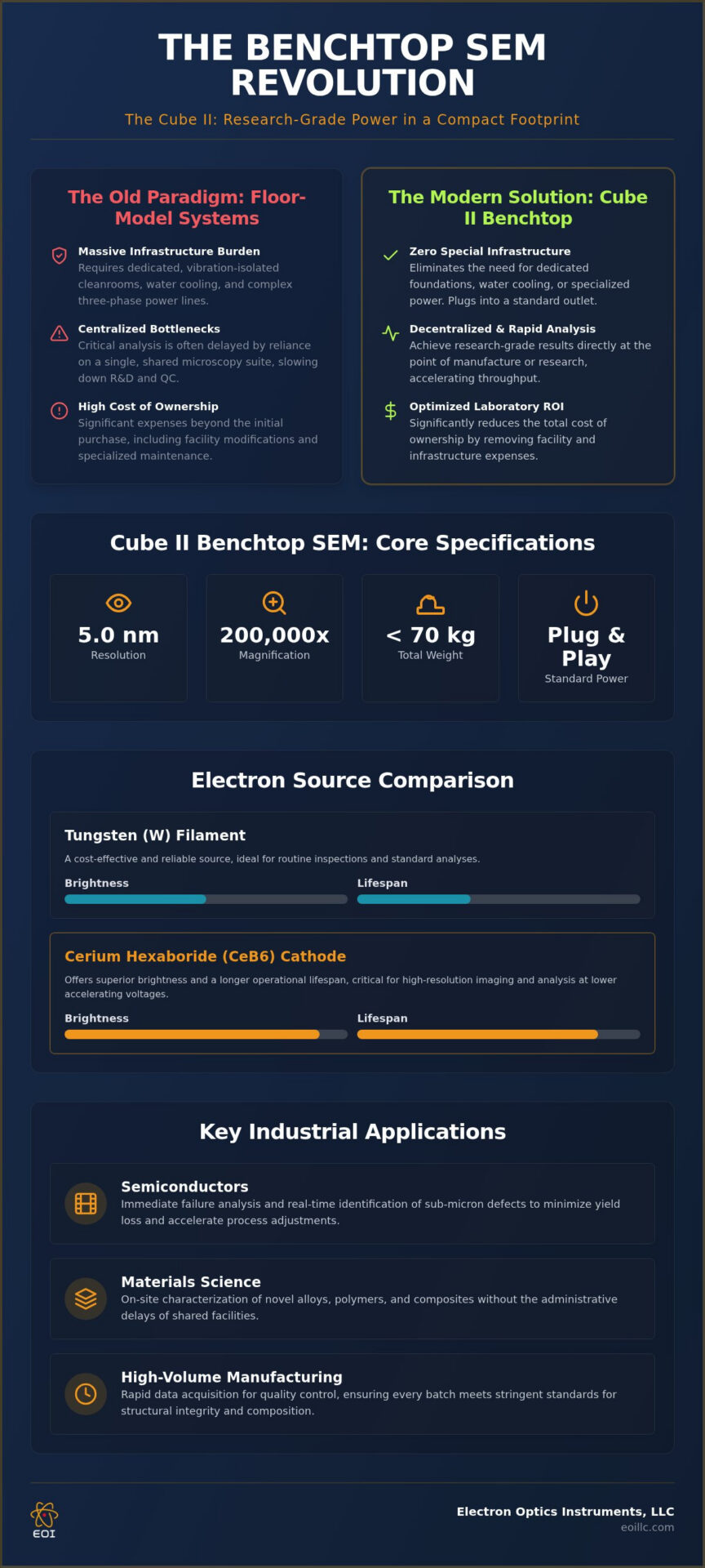
Can a compact instrument weighing less than 70 kilograms truly replicate the analytical depth of a traditional floor-model system? For many industrial laboratories, the necessity of high-resolution imaging has often been met with the harsh realities of limited cleanroom space and the exhausting complexity of legacy optics. It’s a common frustration to see critical failure analysis delayed by the bottlenecks of a centralized microscopy suite. The Cube II Benchtop SEM represents a paradigm shift in this technical landscape, offering a resolution of 5.0 nm and magnification up to 200,000x within a portable footprint that eliminates the need for dedicated vibration isolation foundations.
You likely recognize that maintaining a competitive edge requires rapid, on-site characterization without the burden of specialized facility modifications. This guide explores how modern desktop SEM technology provides research-grade imaging with reduced infrastructure requirements and optimized laboratory ROI. We’ll analyze the total cost of ownership for these advanced systems and detail the specific technical integrations, such as Energy Dispersive Spectroscopy, that allow the Cube II to deliver faster throughput for complex industrial applications.
Key Takeaways
- It’s now possible to eliminate the need for specialized infrastructure such as water cooling and vibration-isolated cleanrooms while significantly reducing the total cost of ownership.
- Evaluate the performance differences between Tungsten and Cerium Hexaboride electron sources to determine the optimal analytical resolution for your specific industrial samples.
- Discover the specific capabilities of the Cube II Benchtop SEM, which delivers research-grade imaging up to 200,000x magnification in a compact, portable footprint.
- Apply a strategic framework for matching laboratory requirements with the appropriate Veritas or Genesis series models based on sample conductivity and required throughput.
- Gain insights into essential maintenance protocols that ensure long-term precision and maximize the operational lifecycle of your electron optics investments.
The Evolution of Desktop SEM: Redefining Laboratory Capabilities in 2026
The modern desktop Scanning Electron Microscope (SEM) represents a fundamental departure from the resource-intensive architectures of the previous decade. By 2026, these instruments have transitioned from secondary screening tools to primary analytical assets, housing high-performance electron optics within a self-contained, vibration-isolated chassis. This evolution reflects a broader industry shift toward decentralized research environments where localized imaging capabilities are essential for maintaining rigorous production timelines. Instead of relying on centralized microscopy suites that require specialized facilities, modern laboratories utilize systems like the Cube II Benchtop SEM to achieve research-grade results directly at the point of manufacture, effectively democratizing high-resolution analysis across diverse industrial sectors.
The Shift from Floor-Model to Benchtop Architectures
The physical downsizing of electron microscopy is primarily driven by the radical simplification of vacuum system engineering and the integration of micro-positioning stages. Modern benchtop units utilize compact, high-efficiency turbomolecular pumps that achieve operational vacuum levels in minutes, bypassing the massive footprints or external water-cooling requirements typical of legacy floor-model systems. This reduction in mechanical complexity doesn’t compromise imaging quality; rather, it focuses on maximizing the performance of the electron column within a more efficient spatial envelope. The transition to plug-and-play power requirements allows these instruments to operate on standard wall outlets, eliminating the need for complex electrical infrastructure or dedicated three-phase power lines. The Cube II Benchtop SEM, providing a resolution of 5.0 nm and magnification up to 200,000x, serves as a strategic tool for high-throughput environments in 2026, offering a sophisticated balance between technical precision and spatial economy.
Key Industrial Drivers for Desktop SEM Adoption
In the semiconductor sector, the demand for immediate failure analysis has made the desktop SEM an indispensable component of the quality control workflow. As feature sizes continue to shrink, the ability to identify sub-micron defects in real-time allows for rapid process adjustments that minimize yield loss. Materials science research similarly benefits from this democratization of high-level imaging. Researchers can now perform on-site characterization of novel alloys and polymers without the administrative delays associated with shared facility booking. High-volume manufacturing environments prioritize these systems for their rapid data acquisition capabilities, ensuring that every batch meets stringent international standards for structural integrity and elemental composition. By integrating these advanced hardware systems, organizations achieve a synergy between ecological responsibility and industrial performance, reducing their physical footprint while elevating their analytical standards.
Core Technical Specifications: Navigating Electron Sources and Analytical Integration
The efficacy of a benchtop system is fundamentally defined by its electron source and detector configuration. Tungsten filaments remain a staple for their cost-effectiveness and reliability in routine inspections. However, Cerium Hexaboride (CeB6) cathodes provide superior brightness and a longer operational lifespan, which is critical for high-resolution imaging at lower accelerating voltages. The Cube II Benchtop SEM leverages these advancements to deliver a resolution of 5.0 nm, effectively bridging the gap between portable convenience and the rigorous demands of industrial research. This technical balance ensures that decentralized laboratories can maintain the same analytical standards as centralized facilities.
Variable pressure (VP) modes represent a critical advancement for analyzing non-conductive samples without the need for gold or carbon sputter coating. By introducing a controlled amount of gas into the chamber, the system neutralizes surface charging that would otherwise obscure detail. This capability is often paired with a Backscattered Electron (BSE) detector to highlight compositional differences through atomic number contrast; meanwhile, the Secondary Electron (SE) detector captures intricate surface topography. The synergy between these detectors allows for a holistic understanding of sample morphology and material distribution.
Understanding Resolution and Magnification Thresholds
It’s essential to distinguish between digital magnification and the actual optical resolution limits of the instrument. While many systems claim high magnification numbers, the true metric of performance is the ability to resolve two distinct points at the nanometer scale. Modern units like the Cube II achieve resolutions that rival older floor models by optimizing the electron column and utilizing sophisticated signal processing. Adjusting the accelerating voltage allows operators to balance image clarity with the risk of sample damage, ensuring the depth of field is appropriate for the specific material under review.
Integrated EDS and Analytical Capabilities
Quantitative elemental mapping is facilitated through Energy Dispersive Spectroscopy (EDS). This integration allows for the simultaneous acquisition of morphological data and chemical composition, transforming the SEM into a comprehensive analytical platform. For more detail on the underlying physics, you may review The Fundamental Principles of Scanning Electron Microscopy (SEM) in 2026. Choosing between integrated and add-on EDS systems depends on your throughput requirements and the complexity of the materials being analyzed. If your laboratory requires high-precision elemental data, exploring the advanced analytical configurations offered by Electron Optics Instruments can optimize your technical workflow.
The Benchtop Advantage: Infrastructure, ROI, and Operational Efficiency
The economic justification for integrating a benchtop system centers on the drastic reduction in indirect operational expenses. While floor-model units necessitate a significant initial capital outlay, their total cost of ownership is often inflated by the requirement for specialized facility modifications. These hidden costs include dedicated electrical circuits, reinforced flooring, and complex plumbing for cooling systems. In contrast, the Cube II Benchtop SEM operates with a significantly leaner infrastructure profile, allowing organizations to allocate resources toward analytical personnel rather than facility maintenance. Understanding these financial dynamics is essential for calculating the total cost of ownership for an SEM and ensuring a rapid return on investment. Modern software interfaces also contribute to this efficiency by reducing the training curve for staff, transitioning the instrument from a specialized tool to a standard laboratory asset.
Eliminating Cleanroom and Specialized HVAC Requirements
Modern benchtop architectures are engineered with internal vibration damping that permits operation in standard laboratory or office environments. Unlike their floor-standing predecessors, these systems don’t require external chilled water systems or high-capacity HVAC units to dissipate heat. This office-environment compatibility allows the Cube II Benchtop SEM to be placed directly on existing workbenches, effectively turning any workspace into a high-resolution imaging station. The elimination of cleanroom requirements significantly lowers the barrier to entry for smaller firms and decentralized research departments, fostering a more agile developmental environment.
Workflow Acceleration and High-Throughput Analysis
Operational efficiency is further enhanced by the rapid vacuum cycles inherent in smaller chamber designs. Modern desktop units achieve operational vacuum levels in under 3 minutes, a stark contrast to the lengthy pump-down sequences of large-volume chambers. This speed allows for high-throughput failure analysis and routine quality control without the typical bottlenecks. Automated sample stages further streamline the process, enabling the analysis of multiple specimens in a single programmed sequence. By serving as efficient screening tools, these benchtop systems offload routine work from core microscopy facilities, ensuring that the most complex instruments are reserved for specialized research while the Cube II handles the high-volume demand of daily industrial production.
Strategic Selection: Matching Desktop SEM Models to Industrial Requirements
Selecting the appropriate instrument requires a methodical evaluation of the sample’s physical properties and the desired analytical outcome. For many organizations, the Cube II Benchtop SEM serves as the optimal baseline for high-resolution imaging, providing a robust 5.0 nm resolution that fulfills the majority of industrial requirements. However, more complex applications involving advanced SEM techniques for nanotechnology may necessitate specialized configurations. The decision matrix should prioritize the intersection of resolution, chamber volume, and automation capabilities to ensure the hardware aligns with long-term corporate strategy.
A frequent objection to benchtop adoption involves the analysis of non-conductive, un-coated materials. Modern units address this through sophisticated variable pressure modes and low-vacuum detectors, allowing for the direct imaging of polymers or biological specimens without the structural artifacts associated with traditional sputter coating. This capability ensures that delicate samples remain in their native state for more accurate characterization. It’s a critical factor for labs transitioning from routine inspections to advanced materials research where surface integrity is paramount.
SEM for Failure Analysis and Quality Control
In the context of failure analysis and quality control, throughput and chamber volume are the primary metrics for success. The Veritas Series SEM is engineered for these high-demand environments, offering expanded chambers that accommodate industrial components without the necessity of destructive sectioning. These systems excel at semiconductor inspection and particle analysis, where identifying the root cause of a defect requires both speed and precision. Automated scripting for repetitive QC tasks allows operators to define specific regions of interest across multiple samples, ensuring consistent data collection while minimizing human error and maximizing the efficiency of the analytical workflow.
High-Resolution Imaging for Nanomaterials
The emergence of Field-Emission (FE) sources in the desktop category has been transformative for nanomaterials research. For structures like carbon nanotubes, intricate polymers, and complex biological matrices, the beam stability of an FE source is indispensable. Instruments such as the Veritas FE SEM provide the ultra-high resolution required to resolve sub-nanometer features that were previously only visible on massive floor-model systems. Adhering to the professional guide to SEM operation ensures that users can maximize these technical capabilities in a research setting. To determine which configuration best supports your specific production standards, you can request a technical consultation with the experts at Electron Optics Instruments.
The Electron Optics Advantage: Lifecycle Support and Technical Excellence
Electron Optics Instruments, LLC has spent 30 years establishing its position as a premier technical authority in the scanning electron microscopy sector. By curating a sophisticated portfolio that includes the Cube II Benchtop SEM, Genesis, and Veritas Series, the organization provides a comprehensive spectrum of solutions tailored to modern industrial requirements. This leadership isn’t merely about hardware; it’s about the intersection of visionary innovation and the practical realities of international production. For organizations looking to manage their laboratory ROI more aggressively, the availability of high-quality Refurbished SEM Units provides a strategic entry point into advanced characterization. These systems undergo rigorous validation to ensure they meet the same superior standards as new equipment, reflecting the brand’s commitment to reliability and technical meticulousness.
Cube II and Veritas: Precision Engineering for the Modern Lab
As the sole US distributor for EmCraft Scanning Electron Microscopes, Electron Optics Instruments offers exclusive access to the Cube II Benchtop SEM. This instrument has become a cornerstone of decentralized research, providing a unique balance of portability and research-grade resolution. While the Cube II serves as a flagship for benchtop performance, the Veritas Pro and Veritas Ultra series are designed for high-end analytical requirements that necessitate advanced detector integration and superior beam stability. These systems represent the pinnacle of tabletop architecture, allowing partners to push the boundaries of what’s possible in hardware integration. Whether your facility prioritizes the rapid sample exchange of the Genesis or the ultra-high resolution of the Veritas FE SEM, the goal is always to achieve a synergy between technical prowess and logistical excellence.
Comprehensive Field Service and Professional Training
Maintaining the precision of an electron column over its entire lifecycle requires a disciplined approach to definitive SEM maintenance. Multi-tiered service contracts and Preventative Maintenance Visits are essential components of a strategy designed to maximize the longevity of your investment. Our field service engineers don’t just perform routine checks; they provide deep technical insights that help optimize your specific workflows. On-site training programs are structured to bridge the gap between complex legacy optics and modern automated interfaces, ensuring your staff can leverage every feature of the instrument. From professional decommissioning to the relocation of sensitive optics, the focus remains on providing a wealth of information and support that reinforces our status as a high-tech authority in the national landscape.
Advancing Industrial Characterization Through Desktop Innovation
The transition toward decentralized, high-resolution imaging is no longer a future projection but a present industrial reality. By integrating systems like the Cube II Benchtop SEM, laboratories can achieve nanometer-scale resolution while eliminating the prohibitive costs of specialized infrastructure and cleanroom modifications. This strategic shift facilitates faster failure analysis and more rigorous quality control directly at the production site, ensuring that technical meticulousness remains a core component of your operational workflow. It’s a transformation that balances sophisticated analytical power with the practical requirements of modern manufacturing.
Success in this technical landscape depends on more than hardware alone; it requires a partnership with a seasoned global innovator. With over 30 years of industry expertise and a comprehensive national service network, Electron Optics Instruments provides the lifecycle support necessary to maintain peak optical performance and long-term precision. Whether you require the advanced analytical depth of the Veritas series or specialized on-site technical training, our team’s committed to your long-term success. Request a Technical Consultation for Your Desktop SEM Requirements and ensure your laboratory is equipped with the pinnacle of modern microscopy.
Frequently Asked Questions
What is the typical resolution of a desktop SEM compared to a floor model?
Modern desktop systems achieve resolutions that rival many older floor-standing units. For instance, the Cube II Benchtop SEM offers a resolution of 5.0 nm, which is sufficient for the vast majority of industrial failure analysis and materials characterization tasks. While high-end floor models still lead in sub-nanometer imaging, desktop units provide research-grade clarity without the infrastructure burden, effectively bridging the gap for most laboratory applications.
Does a desktop SEM require a specialized vacuum environment or vibration-proof room?
Desktop SEMs don’t require specialized cleanrooms or vibration-isolated foundations. Most systems, including the Veritas Series, feature internal damping and compact, high-efficiency vacuum pumps. They’re designed for office-environment compatibility and can operate on standard workbenches. This mobility allows decentralized labs to perform high-level imaging without the complex HVAC or plumbing modifications typically required by legacy floor models used in previous decades.
Can a desktop SEM perform Energy Dispersive Spectroscopy (EDS) for elemental analysis?
Yes, desktop systems can be fully integrated with Energy Dispersive Spectroscopy hardware for comprehensive elemental analysis. This integration allows operators to perform morphological inspections and chemical characterization simultaneously within a single workflow. The Cube II is compatible with EDS systems from major manufacturers like Oxford and Bruker. Such analytical depth is essential for identifying contaminants or verifying alloy compositions in semiconductor and manufacturing sectors.
How long does it take to train a new operator on a benchtop SEM system?
Training a new operator typically takes only a few hours to a couple of days due to intuitive, modern software interfaces. Modern systems automate complex tasks like focus, brightness, and contrast adjustment, which reduces the technical barrier to entry. Electron Optics Instruments provides on-site technical training to ensure laboratory staff can maximize equipment utility quickly. This efficiency contrasts sharply with the weeks of specialized expertise required for legacy optics.
What are the maintenance requirements for a desktop scanning electron microscope?
Maintenance involves routine tasks like filament replacement and vacuum system checks to ensure peak performance. It’s critical to schedule Preventative Maintenance Visits to ensure long-term precision and prevent unexpected downtime. Consumables such as apertures and filaments must be monitored regularly for wear. Professional service contracts provide the technical support and parts coverage needed to ensure the instrument continues to meet its original factory specifications.
Can I use a desktop SEM for non-conductive or biological samples without coating?
Desktop SEMs can image non-conductive samples without gold or carbon coating when equipped with variable pressure modes. This mode introduces a controlled gas environment to neutralize surface charging that often obscures detail. It’s ideal for polymers, biological structures, and delicate materials that might be damaged by traditional sputter coating. Using backscattered electron detectors in these modes provides excellent compositional contrast on native, untreated specimens.
What is the price range for a new vs. refurbished desktop SEM in 2026?
Pricing for desktop SEMs varies significantly based on configuration, resolution, and integrated analytical tools like EDS. While new systems reflect the latest advancements in hardware integration, Refurbished SEM Units offer a cost-effective gateway to high-resolution microscopy for budget-conscious facilities. Organizations should evaluate their specific imaging requirements and throughput needs when deciding between these options. Consulting with an authorized distributor is the best way to determine the optimal investment.
How does the vacuum pump-down time of a desktop SEM compare to traditional units?
Vacuum pump-down times for desktop units are significantly faster than traditional floor models, often reaching operational levels in under 3 minutes. The smaller chamber volume allows high-efficiency turbomolecular pumps to reach vacuum rapidly. This efficiency enables higher throughput for failure analysis and routine quality control by reducing the wait time between samples. Faster cycles mean more specimens can be analyzed per shift, directly optimizing the laboratory ROI.