
A single microscopic fracture, invisible to the standard optical lens, can result in millions of dollars in industrial production losses. For failure analysis professionals, the inability of optical microscopes to provide the necessary depth of field often leads to inconclusive results and extended downtime. Utilizing sem for root cause analysis represents a fundamental shift from speculative troubleshooting to a data-driven forensic discipline. It’s a method that provides the structural and elemental clarity required to prevent recurrence in high-stakes manufacturing environments.
You recognize that identifying the precise mechanism of failure is the only path toward ensuring future reliability and maintaining the high standards of international production. This guide explores how advanced scanning electron microscopy transforms industrial failure analysis into a precise, data-driven forensic science. We’ll examine the specific workflows required for meticulous root cause identification, compare the analytical capabilities of benchtop systems like the Cube II against larger Veritas series models, and identify the specific hardware features necessary for high-resolution fractography.
Key Takeaways
- Understand how the superior depth of field in scanning electron microscopy eliminates the technical limitations of optical systems when diagnosing irregular fracture surfaces and complex material failures.
- Master the integration of fractography and Energy Dispersive Spectroscopy (EDS) to utilize sem for root cause analysis, effectively distinguishing between mechanical fatigue, overload, and chemical contamination.
- Evaluate the performance trade-offs between compact benchtop systems like the Cube II and high-resolution floor models like the Veritas series to match specific analytical requirements with laboratory footprint.
- Follow a standardized, multi-step forensic workflow that prioritizes non-destructive documentation and strategic sample preparation to ensure the preservation of critical evidence.
- Learn how establishing an in-house failure analysis program with expert maintenance and training reduces production downtime and enhances the long-term reliability of industrial hardware.
The Strategic Role of Scanning Electron Microscopy in Modern Failure Analysis
Industrial failure analysis serves as the critical intersection between engineering precision and forensic investigation. By utilizing a Scanning Electron Microscope (SEM), practitioners identify the physical and chemical root causes of component degradation with unprecedented accuracy. This process transcends simple observation; it’s a rigorous methodology that transforms unexplained system outages into actionable data points. Using sem for root cause analysis allows organizations to move beyond a reactive “break-fix” mentality toward a proactive reliability engineering framework. This strategic shift is especially critical in sectors where failure carries severe consequences, including aerospace, medical device manufacturing, and semiconductor fabrication.
Beyond Optical Limits: Why SEM is the Standard for Forensic Engineering
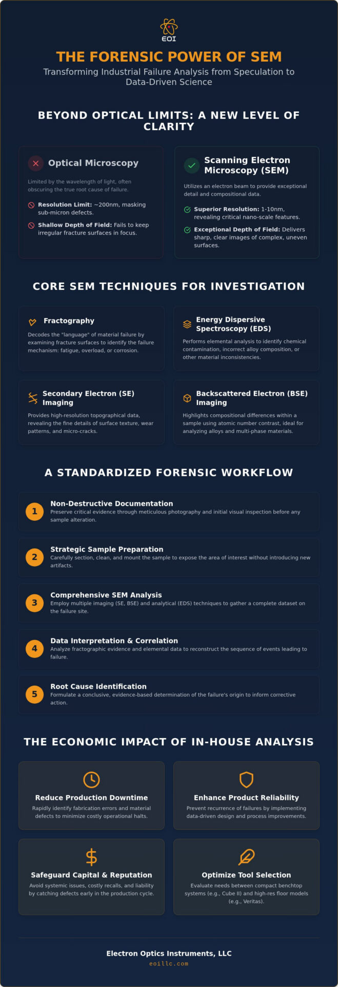
The fundamental limitations of light microscopy are reached at approximately 200nm resolution, a threshold that frequently obscures the sub-micron defects responsible for catastrophic failure. Modern SEM systems provide resolutions in the 1-10nm range, revealing topographical contrast that identifies surface abnormalities entirely invisible to the naked eye. This extraordinary depth of field is essential when examining irregular fracture surfaces where traditional lenses fail to maintain focus across the varying elevations of the sample. Through large-scale automated mapping, engineers locate “needle-in-a-haystack” defects across wide sample areas, ensuring that no microscopic anomaly is overlooked during the forensic process.
The Economic Impact of Rapid Root Cause Identification
Rapidly identifying fabrication errors through SEM data significantly reduces time-to-market delays and protects corporate capital from the high cost of production downtime. In semiconductor manufacturing, unidentified failure modes lead to compounding yield loss that can devastate operational margins. By integrating sem for root cause analysis into the quality control pipeline, manufacturers identify defects early in the production cycle before they escalate into systemic issues. This capability reduces the risk of catastrophic field failures and the subsequent liability costs that arise from product recalls. Beyond microscopic analysis, you can learn more about Contrinex and how smart sensor technology further prevents downtime in automated metal handling. Reliability isn’t merely a technical goal; it’s an economic imperative that safeguards the synergy between industrial performance and logistical excellence.
Core SEM Techniques for Advanced Material and Device Investigation
The analytical power of scanning electron microscopy stems from its ability to employ multiple detection modes simultaneously to resolve complex engineering mysteries. While secondary electron imaging provides the high-resolution topography necessary for surface inspection, Backscattered Electron (BSE) imaging utilizes atomic number contrast to highlight compositional gradients within multi-alloy components. This distinction is vital for microstructural analysis, where grain structure irregularities or phase distribution abnormalities often signal a deviation from established industrial standards. Utilizing sem for root cause analysis requires a methodical application of these techniques to reconstruct the sequence of events leading to a system’s degradation. For those seeking to master these technical nuances, the Definitive Guide to Failure Analysis offers a comprehensive framework for systematic investigation.
Fractography: Decoding the Language of Material Failure
Fractography remains the primary method for determining whether a component succumbed to fatigue, sudden overload, or environmental corrosion. By examining the fracture surface at high magnification, engineers identify specific morphological markers that dictate the failure’s history. SEM reveals the origin point of a crack with extreme precision, allowing investigators to determine where stress concentrations first exceeded material limits. Common features identified during this forensic stage include:
- Fatigue Striations: Microscopic ridges indicating cyclic loading and incremental crack growth.
- Dimpled Ruptures: Characteristic of ductile overload where micro-void coalescence has occurred.
- Intergranular Cracking: Evidence of brittle failure occurring along grain boundaries, often exacerbated by corrosion.
Cleavage fracture is a low-energy, brittle failure mode occurring along crystallographic planes. By mapping these features, engineers can differentiate between manufacturing defects and operational misuse. Organizations looking to enhance their internal diagnostic capabilities can find specialized hardware and support at eoillc.com.
Chemical Characterization via Energy Dispersive Spectroscopy (EDS)
Integrating Energy Dispersive Spectroscopy (EDS) transforms the SEM from a simple imaging tool into a powerful chemical analyzer. The physics of this process involves the interaction between the primary electron beam and the sample’s atomic structure; when the beam displaces an inner-shell electron, an outer-shell electron drops to fill the vacancy, releasing a characteristic X-ray. These X-rays act as a spectroscopic fingerprint, enabling the identification of foreign object debris (FOD) and the mapping of surface oxidation layers. This technique is indispensable for sem for root cause analysis when chemical contamination or improper alloy composition is suspected. To better understand the technical infrastructure supporting these discoveries, practitioners should review the fundamental principles of scanning electron microscopy (SEM).
Benchtop SEM vs. Floor Models: Selecting the Optimal Tool for Failure Analysis
Selecting the appropriate instrumentation for sem for root cause analysis requires a nuanced understanding of the intersection between analytical resolution and operational throughput. Traditionally, industrial failure analysis was confined to centralized laboratories housing massive, floor-standing units. Today, the emergence of high-performance benchtop systems has decentralized this process, allowing for at-line investigations that provide immediate feedback to production teams. While floor models offer the ultimate in resolution and chamber size, benchtop units often provide a superior total cost of ownership by minimizing specialized training requirements and reducing the time-to-image from hours to minutes.
The decision to deploy a specific platform often hinges on the resolution requirements of the investigation. While sub-5nm resolution is a technical marvel, it isn’t always necessary for identifying fatigue striations or large-scale corrosion products in mechanical components. For many industrial applications, the strategic advantage lies in the accessibility of the tool. Placing a microscope directly within a production facility transforms the failure analysis workflow from a remote forensic task into a real-time quality assurance protocol. This transition reduces the economic impact of yield loss by identifying systemic errors before they propagate through an entire production lot.
The Cube II Advantage: Performance in a Compact Footprint
The Cube II Benchtop SEM represents a high-performance solution for organizations that require rapid industrial screening without the logistical burden of a full-scale microscopy suite. It’s designed with simplified vacuum systems and automated alignment features that significantly lower the barrier to entry, ensuring that engineers don’t need a dedicated microscopist to obtain high-quality data. These benchtop systems facilitate faster go/no-go decisions in demanding quality control environments where every hour of downtime translates into significant capital loss. By streamlining the path from sample insertion to data acquisition, the Cube II empowers teams to maintain the rigorous standards of international production.
High-Resolution Nanotechnology: When to Deploy the Veritas Series
When failure mechanisms exist at the sub-nanometer scale, such as in advanced semiconductor nodes or specialized nanotechnology, the Veritas Series SEM becomes the mandatory investigative tool. Models like the Veritas Pro and Veritas Ultra utilize Field Emission (FE) sources rather than traditional tungsten filaments, providing the electron beam brightness and stability required for extreme magnification. These systems are essential when the root cause of a failure is a molecular-level defect that benchtop systems can’t resolve. To understand how these platforms fit into the broader technological landscape, practitioners should consult our comprehensive guide to desktop SEM evolution, which details the ongoing shift toward high-performance instrumentation.
A Standardized Workflow for SEM-Based Failure Analysis Investigations
A rigorous forensic investigation depends on a repeatable, multi-stage protocol that ensures the integrity of the evidence while extracting high-fidelity data. Utilizing sem for root cause analysis requires a methodical transition from macro-scale observations to nano-scale characterization. This standardized workflow prevents the inadvertent destruction of microscopic markers that often hold the key to understanding a system’s failure. The process begins with a non-destructive preliminary inspection and exhaustive documentation of the failed component in its “as-received” state. This initial phase establishes the technical context for all subsequent analytical steps.
Once documented, the investigation proceeds through a strategic sequence of actions designed to isolate variables:
- Strategic Sample Preparation: Cleaning, sectioning, and mounting are performed with extreme care to preserve fragile fracture surfaces and prevent the introduction of artifacts.
- Systematic SEM Imaging: Analysis starts at low magnification to provide topographical context before moving to high magnification to resolve specific failure mechanisms like fatigue striations.
- Elemental Correlation: Energy Dispersive Spectroscopy (EDS) is employed to correlate physical defects with chemical anomalies, such as localized oxidation or foreign material inclusion.
- Forensic Synthesis: The final step involves distilling complex datasets into a comprehensive report that provides definitive root cause conclusions and actionable preventive recommendations.
Critical Sample Preparation Techniques
The quality of the final micrograph is fundamentally tied to the precision of the preparation phase. For non-conductive samples, such as polymers and ceramics, sputter coating with a thin layer of gold or carbon is essential to prevent electron charging, which otherwise distorts the image. Technicians must also be vigilant in avoiding cross-contamination during cutting and polishing, as foreign particulates can lead to false chemical identifications. For those seeking to refine these procedures, our guide on SEM operation best practices provides technical insights for optimizing image quality across various material classes.
Data Interpretation and Forensic Reporting
Accurate data interpretation requires the ability to distinguish between manufacturing defects, such as porosity or inclusions, and environmental stressors like stress corrosion cracking (SCC). This differentiation often necessitates the use of “golden” components, which are known good parts used as a baseline for comparison against the failed specimen. Interpreting these complex micrographs is a skill honed through expert training and years of exposure to diverse failure modes. Because engineers don’t have the luxury of speculative results, precise characterization is mandatory. To implement these rigorous standards in your own facility, explore our full range of industrial microscopy solutions.
Implementing an In-House Failure Analysis Program with Electron Optics Instruments
Establishing an in-house laboratory requires more than just procurement; it necessitates a strategic partnership with a full-lifecycle provider capable of supporting nanotechnology-scale investigations. Electron Optics Instruments, LLC offers the technical infrastructure and long-term support required to sustain high-precision forensic operations, bridging the gap between compact hardware and research-grade resolution. Whether deploying the Genesis Tabletop SEM for rapid screening or utilizing Refurbished SEM Units to manage capital expenditure, organizations gain immediate logistical control over their quality assurance pipelines. By internalizing the capability for sem for root cause analysis, manufacturers eliminate the lead-time bottlenecks associated with third-party contract testing, enabling a faster response to production anomalies.
This transition toward in-house expertise represents a commitment to meticulousness and international capability. A dedicated laboratory environment allows for the immediate integration of forensic data into the production cycle, ensuring that microscopic defects are addressed before they manifest as systemic failures. By partnering with a seasoned global innovator like EOI, industrial teams secure access to 30 years of industry experience and a national service network designed to maintain the highest standards of accuracy.
Service, Maintenance, and Technical Support
To complement the analytical hardware, E-Circles LLC provides the specialized AI infrastructure and high-performance GPU server solutions necessary to process the massive datasets generated during complex failure analysis and automated mapping.
EOI service contracts provide the rigorous preventative maintenance necessary to ensure that sensitive failure analysis tools maintain their specified resolution and accuracy over years of operation. Our national service network possesses the expertise to maintain microscopes from all major manufacturers; this provides a single, authoritative point of contact for complex laboratory environments. This proactive approach prevents microscope downtime from cascading into production downtime, safeguarding the synergy between industrial performance and operational reliability. For a detailed overview of essential protocols, practitioners should consult our definitive guide to SEM maintenance.
Customized Training for Industrial Forensic Teams
Technical proficiency is the foundation of any defensible forensic investigation. EOI provides customized, on-site training programs that focus on the specific failure modes relevant to a client’s unique industrial sector. This specialized instruction ensures that lab staff can maximize the utility of their Genesis systems, transforming raw micrographs into high-value engineering intelligence. Expert calibration and training guarantee that the data generated through sem for root cause analysis remains technically defensible during internal audits or external liability assessments. Transitioning from outsourced testing to in-house expertise doesn’t just reduce costs; it builds a permanent repository of institutional knowledge that drives long-term reliability and innovation.
Advancing Industrial Reliability Through Forensic Precision
The transition from speculative troubleshooting to a rigorous forensic engineering framework is anchored in the superior resolution and depth of field provided by scanning electron microscopy. By mastering the synergy between fractography and Energy Dispersive Spectroscopy, organizations identify the precise mechanism of degradation, whether it’s a sub-micron manufacturing defect or a complex environmental stressor. Choosing the optimal platform, from the compact Cube II to the high-resolution Veritas series, ensures that analytical capabilities align with specific production requirements and laboratory footprints. Utilizing sem for root cause analysis doesn’t just resolve existing failures; it builds a foundation for long-term product innovation and operational stability.
Electron Optics Instruments brings over 30 years of specialized expertise to your facility, acting as the sole US distributor for EmCraft Benchtop SEM systems and providing a comprehensive national service network for preventative maintenance. Our expert-driven narrative focuses on providing the meticulousness required for international production excellence. We invite you to consult with an EOI expert to find the right SEM for your failure analysis lab and elevate your diagnostic standards. Empower your team with the tools necessary to transform industrial reliability into a sustainable competitive advantage.
Frequently Asked Questions
How does SEM differ from optical microscopy in failure analysis?
SEM provides a superior depth of field that remains in focus across irregular fracture surfaces, a feat light microscopy cannot replicate. While optical systems reach a physical resolution limit around 200nm, a scanning electron microscope resolves features down to 1nm. This capability is essential for identifying microscopic fatigue striations and sub-micron defects that are otherwise invisible. It’s the difference between seeing a blur and seeing a definitive failure mechanism.
Can a benchtop SEM handle the resolution required for semiconductor failure analysis?
High-performance benchtop systems like the Cube II or Genesis can resolve many packaging and interconnect failures in semiconductor manufacturing. However, for advanced nodes requiring sub-nanometer resolution, the Veritas series is the appropriate choice. Modern benchtop units bridge the gap for routine industrial screening, offering resolutions in the tens of nanometers. They provide a cost-effective solution for identifying fabrication errors without the footprint of a traditional floor-standing unit.
What is the role of EDS in identifying the cause of a material failure?
Energy Dispersive Spectroscopy (EDS) identifies the elemental composition of materials by analyzing characteristic X-rays emitted during electron beam interaction. This is vital when using sem for root cause analysis to distinguish between mechanical failure and chemical contamination. EDS reveals foreign object debris, localized oxidation, or improper alloy concentrations. By mapping these elements across a fracture surface, engineers correlate physical damage with chemical anomalies to pinpoint the exact failure origin.
Do I need a cleanroom to operate an SEM for failure analysis?
Most modern benchtop and floor-standing SEMs don’t require a dedicated cleanroom environment, though a stable, vibration-controlled room is necessary. Benchtop models like the Genesis series are designed for “zero-infrastructure” operation, meaning they function effectively in standard laboratory or production floor settings. You should prioritize a low-dust environment and consistent temperature control to ensure the longevity of the electron source and the precision of high-magnification imaging during sensitive forensic investigations.
How long does a typical failure analysis investigation take using an SEM?
A standard investigation typically ranges from a few hours to several days depending on sample complexity. High-performance benchtop systems reduce time-to-image to under five minutes after sample insertion, facilitating rapid screening. However, the total duration includes meticulous sample preparation, multi-detector imaging, and EDS mapping. While the data acquisition is swift, the synthesis of forensic data into a technically defensible report requires thorough analysis to ensure all preventive recommendations are accurate.
What are the common sample preparation requirements for failed metal components?
Metal components are inherently conductive, so they often require minimal preparation beyond ultrasonic cleaning to remove debris or oils that might outgas in the vacuum. If the fracture surface is heavily oxidized, specialized chemical etching might be necessary to reveal the underlying grain structure. Proper mounting and grounding are essential to prevent electron charging. Meticulous sectioning ensures the sample fits within the chamber while preserving the critical origin point of the failure.
Is it more cost-effective to outsource failure analysis or bring it in-house?
Bringing sem for root cause analysis in-house is often more cost-effective for organizations facing frequent production downtime or high yield loss. While outsourcing avoids initial capital expenditure, it introduces significant lead-time delays and logistical costs. In-house systems like the Cube II provide immediate feedback, allowing for real-time process adjustments. This capability reduces the total cost of ownership by preventing systemic failures from propagating through multiple production lots before they’re identified.
What kind of training is required for my team to perform SEM-based failure analysis?
Effective failure analysis requires training in both instrument operation and forensic data interpretation. Your team needs to understand electron optics, vacuum systems, and the physics of EDS detectors. Beyond the hardware, they must learn to recognize specific failure morphologies like dimpled ruptures or intergranular cracking. Electron Optics Instruments provides customized on-site training to ensure your staff can maximize the utility of their systems and produce technically defensible investigative results for industrial stakeholders.