

The assumption that higher resolution always equates to superior analytical value is a costly misconception that frequently stalls industrial throughput in 2026. While the pursuit of atomic-scale clarity is understandable, the logistical bottleneck of complex sample preparation and the staggering infrastructure requirements of traditional systems often obscure the practical utility of an instrument. You likely recognize the tension between the need for deep structural insights and the reality of limited lab footprints, especially when evaluating the sem vs tem trade-off. Selecting the wrong microscopy path doesn’t just impact your data; it compromises your entire project timeline and budgetary framework.
This authoritative analysis provides a rigorous technical breakdown of the current microscopy landscape, moving beyond basic specifications to evaluate real-world performance and financial viability. We’ll explore the fundamental differences between surface topography and internal morphology, ensuring you understand exactly how each technology interacts with your specific materials. By the end of this guide, you’ll possess a clear cost-to-benefit framework that balances resolution limits with the efficiency of modern benchtop systems, allowing your lab to maintain its competitive edge without unnecessary capital expenditure.
Key Takeaways
- Analyze the fundamental mechanical and imaging differences to determine whether surface topography or internal atomic-level characterization is essential for your specific material analysis.
- Identify the significant operational constraints of each system, contrasting high-throughput “mount and scan” methodologies with the intensive sample preparation protocols inherent to transmission-based imaging.
- Compare the infrastructure impact of various hardware tiers, including the space-saving advantages of high-resolution benchtop SEM units against the specialized environmental demands of traditional floor-standing systems.
- Establish a robust decision-making framework for the sem vs tem choice by evaluating total cost of ownership against the required depth of field and analytical resolution.
- Gain insight into the 2026 market landscape, including how advancements in automation and resolution are making tabletop SEMs increasingly viable for complex industrial research.
The Fundamentals of Electron Microscopy: SEM and TEM Defined
The Electron microscope represents the pinnacle of analytical instrumentation by utilizing accelerated electron beams to bypass the fundamental diffraction limits of visible light. While traditional optical systems are restricted by the wavelength of photons, electron-based systems leverage the significantly shorter de Broglie wavelength of high-energy electrons. This physical advantage allows researchers to achieve magnifications and resolutions that reveal the molecular and atomic architecture of materials. Every modern electron microscope, regardless of its specific modality, operates within a high-vacuum environment to prevent electron scattering by atmospheric molecules; it utilizes precisely calibrated electromagnetic lenses to focus the beam onto the specimen.
The Core Mechanism: Scanning vs. Transmission
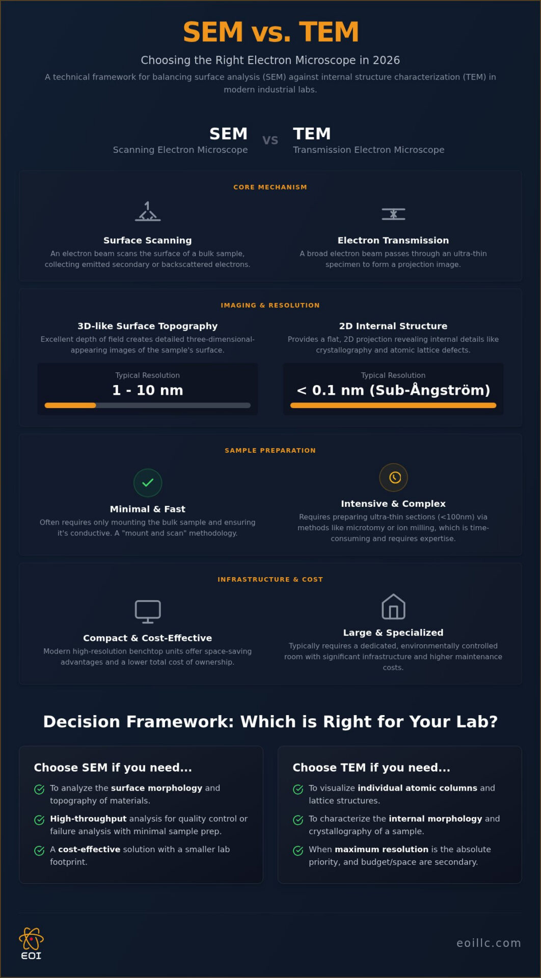
The primary distinction in the sem vs tem paradigm lies in the interaction between the primary electron beam and the specimen. Scanning Electron Microscopy (SEM) utilizes a finely focused probe that raster-scans across the surface of a bulk sample to generate secondary or backscattered electron signals. These signals provide a detailed map of surface morphology and topography, often resulting in images with a characteristic three-dimensional appearance. Conversely, Transmission Electron Microscopy (TEM) directs a broad, coherent beam through an ultra-thin specimen, typically less than 100 nanometers in thickness. The resulting image is a 2D projection of the internal structure, providing unmatched insights into crystallography and lattice defects.
The Evolution of Microscopy in 2026
Industrial laboratories in 2026 are increasingly adopting high-performance desktop SEM solutions to streamline quality control and R&D workflows. These systems benefit from advanced CMOS detectors and sophisticated digital signal processing, which have drastically improved signal-to-noise ratios across all microscopy platforms. This technological maturation has also facilitated correlative microscopy, an integrated approach where the surface data from an SEM is cross-referenced with the internal structural data from a TEM. Such synergy provides a comprehensive material profile that is essential for the development of next-generation semiconductors and advanced polymers.
Understanding the sem vs tem technical divergence is the first step toward optimizing institutional ROI and research accuracy. While both technologies share a common heritage in electron optics, their operational applications serve distinct analytical requirements. Selecting the appropriate instrument requires a meticulous evaluation of whether your data needs favor the external landscape of a sample or its internal crystalline secrets.
Imaging and Resolution: Comparing Technical Capabilities
The technical divergence in the sem vs tem comparison is most apparent when evaluating resolution limits and the resulting depth of field. While standard Scanning Electron Microscopes typically achieve resolutions between 1 and 10 nm, Transmission Electron Microscopes operate at the sub-angstrom level, enabling the visualization of individual atomic columns. This disparity is not merely a matter of magnification; it is a direct consequence of how the electron beam interacts with the specimen. In SEM, the beam penetrates a bulk sample to create a significant interaction volume, where secondary and backscattered signals are generated from a region larger than the initial beam spot. Conversely, the ultra-thin nature of TEM specimens minimizes this volume, allowing the system to maintain the integrity of the electron probe as it passes through the material.
SEM: The King of 3D Surface Morphology
The primary strength of systems like the Veritas Series SEM lies in their ability to capture high-depth-of-field images using Secondary Electrons (SE). These low-energy electrons are emitted from the very top layers of the sample, providing the characteristic topographical contrast that makes SEM the industry standard for fractography and failure analysis. Engineers rely on these 3D-like views to identify the root causes of material fatigue, such as striations or intergranular cracking, which are often invisible in 2D projections. For industrial labs prioritizing rapid surface characterization, exploring the Veritas line offers a path toward superior imaging without the complexity of transmission-based systems.
TEM: Unlocking Atomic-Scale Crystallography
Transmission systems are indispensable when the analytical goal shifts from surface features to internal crystalline arrangements. By utilizing transmitted electrons, TEM allows researchers to observe crystal lattices, dislocations, and grain boundary interfaces at the atomic scale. This capability is augmented by electron diffraction, where the scattering of electrons by the atomic planes of the sample creates patterns used to identify specific material phases and orientations. As noted in this expert breakdown of TEM vs. SEM Imaging, the 2D projection nature of TEM requires a sophisticated understanding of crystallography to interpret the resulting data correctly. This technical depth makes TEM essential for advanced semiconductor fabrication and nanomaterials research where atomic-level precision is the primary requirement for success.
Ultimately, the choice between these capabilities depends on whether your research necessitates the broad topographical context of a bulk sample or the granular, internal structural data of a thin section. While SEM provides the macroscopic “landscape” of a material, TEM delivers the “blueprint” of its atomic construction.
Sample Preparation: The Great Operational Divide
The operational efficiency of a laboratory is often dictated by its specimen preparation protocols rather than the raw imaging power of the hardware. In the sem vs tem analysis, the divergence in specimen requirements represents the most significant hurdle to high-throughput research. While SEM accommodates bulk materials with minimal intervention, TEM mandates specimens that are electron-transparent, typically requiring a thickness of less than 100 nanometers. This fundamental difference transforms the laboratory workflow from a rapid diagnostic cycle into a specialized engineering project. Choosing between these methods requires a realistic assessment of your team’s technical bandwidth and desired turnaround times.
SEM Sample Prep: Speed and Simplicity
The Scanning Electron Microscope excels in environments where time-to-data is a critical performance metric. Standard preparation involves simple mounting on a conductive stub and, for non-conductive materials, a thin sputter coating of gold or carbon to prevent charging. Because SEM can handle samples measuring several inches in diameter, it remains the preferred choice for industrial quality control and failure analysis. To maximize laboratory efficiency, following SEM operation best practices ensures that throughput remains high without sacrificing topographical accuracy. This “mount and scan” workflow allows for the rapid iteration of samples, often providing results within minutes of specimen acquisition.
TEM Sample Prep: The Art of Ultramicrotomy and FIB
Achieving the resolution necessary for atomic characterization requires an intensive and often destructive preparation phase. Technicians must utilize sophisticated techniques such as ion milling, ultramicrotomy, or Focused Ion Beam (FIB) lift-out to isolate a sub-100nm section. These processes aren’t just time-consuming; they often take hours or even days per specimen and require a high degree of technical expertise to avoid preparation artifacts like mechanical deformation or ion beam damage. The complexity of creating these electron-transparent windows means that TEM is generally reserved for targeted, deep-dive research rather than broad-spectrum screening. If your workflow requires analyzing dozens of samples daily, the TEM bottleneck can become a significant institutional liability.
Ultimately, the choice in the sem vs tem debate must account for the human capital and time investment required for each study. While TEM provides unparalleled internal clarity, the sheer simplicity of SEM preparation facilitates a volume of data that transmission systems can’t match in a standard industrial timeline. Balancing these operational realities is essential for maintaining a sustainable and productive research environment.
Infrastructure and Maintenance Requirements
The selection between sem vs tem technologies often hinges on the physical and environmental constraints of the facility rather than purely analytical requirements. A floor-standing TEM is a massive logistical undertaking that typically requires a dedicated, climate-controlled room with high ceilings to accommodate the vertical column. These systems are hypersensitive to floor vibrations and stray magnetic fields; they often necessitate specialized acoustic dampening and electromagnetic shielding. Even minor seismic activity or the proximity of an elevator can distort the sub-angstrom resolution of a TEM beam. Additionally, the high-voltage power supplies used in TEM, often exceeding 200kV, generate significant heat that requires integrated liquid cooling systems and robust electrical infrastructure.
Standard SEM systems offer a far more manageable footprint. While floor-model SEMs still require stable environments, they lack the extreme sensitivity to ambient interference seen in transmission electron optics. The vacuum requirements also differ significantly. TEM columns must maintain ultra-high vacuum levels to prevent electron scattering and filament contamination. Conversely, SEMs operate efficiently at standard high-vacuum or even variable-pressure levels. Understanding the sem vs tem infrastructure gap is critical for long-term ROI, as this operational flexibility makes SEM much easier to integrate into existing industrial workflows without the need for multi-million dollar facility renovations.
The Benchtop Advantage: SEM in Any Lab
The Cube II Benchtop SEM represents a paradigm shift in laboratory integration by eliminating the need for specialized structural modifications. These modern desktop units offer a plug-and-play installation process, requiring only a standard electrical outlet and a sturdy benchtop. Because they operate at lower voltages and utilize efficient thermal management, they don’t require external water chillers or massive power draws. This accessibility allows industrial labs to deploy high-resolution imaging directly on the production floor or within existing research clusters. It’s a visionary approach that prioritizes reliability and space-saving efficiency without compromising the meticulousness of the data. For facilities that must adhere to strict safety protocols in hazardous industrial environments, check out ExSafe for certified power and ventilation equipment.
The complexity of the optical column directly correlates to the frequency and cost of preventative care. Because of their simplified beam paths and lower operating voltages, SEM maintenance is generally more cost-effective and less frequent than the rigorous calibration schedules required for TEM. Professional service contracts are not merely an insurance policy; they’re a technical necessity for maintaining the integrity of the electromagnetic lenses and the vacuum system. Electron Optics Instruments, LLC provides comprehensive, nationwide support for all major electron microscope brands, leveraging 30+ years of industry experience to ensure that your instrumentation remains a reliable asset. If your facility isn’t equipped for the structural demands of a TEM, consult with our technical specialists at Electron Optics Instruments, LLC to explore the Veritas or Cube II series.
Decision Framework: Choosing the Right Microscope for Your ROI
Selecting between sem vs tem platforms requires a rigorous evaluation of your laboratory’s analytical objectives against its logistical and financial capacity. This decision framework operates on a “Resolution vs. Throughput” axis, where the necessity for atomic-scale detail is balanced against the requirement for rapid, repeatable data. In the current 2026 landscape, the emergence of high-performance benchtop systems has disrupted the traditional hierarchy, allowing many industrial facilities to achieve their research goals without the prohibitive total cost of ownership associated with floor-standing transmission units. A visionary lab manager prioritizes an instrument that integrates seamlessly into existing production workflows while maintaining the meticulous standards required for international quality compliance.
When to Choose SEM (and Why Benchtop is Winning)
Scanning Electron Microscopy remains the definitive choice for applications prioritizing surface morphology, particle sizing, and high-volume quality control. The “Benchtop Revolution” has significantly narrowed the performance gap, with instruments like the Cube II Benchtop SEM providing high-resolution imaging that was once the exclusive domain of floor-standing models. These systems are ideal for labs with limited floor space or those that require actionable data in minutes. In sectors such as semiconductor manufacturing and advanced materials development, the industrial ROI of a benchtop SEM is often superior due to its minimal preparation requirements and reduced maintenance overhead. It’s the logical selection for organizations that value technical integration and logistical excellence over the extreme, often unnecessary, resolution of transmission-based systems.
When TEM is Non-Negotiable
The selection between scanning and transmission modalities serves as a critical pivot point for institutional ROI and research precision. While TEM remains the definitive standard for sub-angstrom crystallography, the operational bottlenecks inherent in specimen preparation and facility overhead often favor the high-throughput capabilities of modern scanning systems. A meticulous understanding of the sem vs tem technical divide ensures your laboratory avoids the common pitfall of over-engineering infrastructure at the expense of practical productivity.
Electron Optics Instruments, LLC leverages over 30 years of technical expertise as an authorized EmCraft US distributor to guide your team through these complex procurement cycles. View our full range of Benchtop and Floor-standing SEM solutions to discover how nationwide service and support can secure your laboratory’s long-term analytical capabilities. Your choice of instrumentation should ultimately mirror the grounded realities of your production environment, fostering a culture of innovation through reliable and accurate data acquisition.
Frequently Asked Questions
What is the primary difference between SEM and TEM imaging?
The fundamental distinction in the sem vs tem comparison resides in the interaction of the electron beam with the specimen. SEM focuses on surface topography by collecting secondary or backscattered electrons from bulk samples, providing a pseudo-3D perspective of the material’s exterior. Conversely, TEM directs electrons through an ultra-thin section to capture internal structural data. This divergence dictates whether you visualize the external landscape or the internal blueprint of a material.
Is an SEM or TEM more expensive to operate annually?
Transmission systems incur substantially higher annual operating costs compared to scanning electron microscopes. These expenses stem from the continuous maintenance of ultra-high vacuum environments, the power consumption of high-voltage columns, and the specialized liquid cooling systems required for thermal stability. Additionally, the labor-intensive nature of TEM sample preparation necessitates highly skilled technicians, whereas the “mount and scan” workflow of SEM drastically reduces the labor hours required per specimen analysis.
Can a benchtop SEM achieve the same resolution as a TEM?
A benchtop SEM cannot match the sub-angstrom resolution of a high-end transmission system. While modern instruments like the Cube II Benchtop SEM offer exceptional clarity for surface characterization at the 5nm level, they’re limited by the physics of electron-matter interaction in bulk samples. TEM achieves atomic-scale resolution by utilizing much higher acceleration voltages and transmitted beams, making it the only choice for visualizing individual atomic lattices or molecular structures.
Why does TEM require much thinner samples than SEM?
Transmission Electron Microscopy requires specimens thinner than 100 nanometers because the primary electron beam must physically pass through the material to reach the detector. If the sample exceeds this thickness, the electrons are absorbed or scattered, resulting in an opaque image devoid of structural detail. This necessity for electron transparency is the primary driver behind the complex preparation protocols, such as ultramicrotomy or ion milling, that define standard TEM workflows.
Which microscope is better for elemental analysis (EDS)?
Scanning Electron Microscopy is typically the standard choice for routine elemental analysis and compositional mapping of bulk materials. The larger interaction volume in SEM allows for a higher yield of characteristic X-rays, facilitating rapid Energy Dispersive Spectroscopy (EDS) data collection. While TEM can perform EDS at a much higher spatial resolution, the ultra-thin nature of the samples often limits the total signal intensity, making SEM more efficient for industrial quality control.
What are the infrastructure requirements for installing a TEM?
Installing a TEM requires a sophisticated facility plan that includes a dedicated, high-ceiling room to accommodate the vertical column. The environment must be isolated from floor vibrations and stray electromagnetic fields, which often necessitates specialized acoustic shielding and seismic dampening. Unlike the plug-and-play nature of benchtop SEMs, a TEM also requires integrated liquid cooling loops and a robust electrical infrastructure capable of supporting high-voltage power supplies that often exceed 200kV.
How long does it take to train a technician on SEM vs. TEM?
Training a technician on a modern SEM typically requires several days to a few weeks, especially with the intuitive interfaces found in benchtop units. In contrast, mastering the sem vs tem operational divide requires a significant investment in human capital. TEM proficiency often takes months or even years of specialized study, as the operator must understand complex crystallography, diffraction pattern interpretation, and the meticulous art of electron-transparent sample preparation.
Can I use an SEM to see internal structures of a sample?
A standard SEM cannot visualize the internal morphology of a specimen because it relies on signals reflected or emitted from the surface layers. To view internal features using SEM, the sample must be physically cross-sectioned or fractured to expose its interior for surface scanning. If your research necessitates non-destructive imaging of internal grain boundaries or atomic defects, a transmission system is the only instrument capable of providing that specific structural data.